
12
Electrically Conductive Coatings
In this chapter we discuss a number of aspects of electrically conductive coatings. This type of coatings can be based on either a conductive polymer matrix or on conductive particles in a nonconductive matrix, the latter often being addressed as conductive composite coatings. The former category includes conjugated polymers, such as polypyrrole, and charge transfer compounds, such as TCNQ, while for the latter category a whole gamut of particles can be used, ranging from metals via oxides to carbon‐based materials such as carbon black (CB), carbon nanotubes (CNTs), and graphene. We first briefly describe some typical applications, then address the relevant measuring techniques, and thereafter discuss conductive coatings, limiting the discussion to intrinsically conductive polymers and conductive composite coatings.
12.1 Typical Applications
Both coatings with a low conductivity and high conductivity are used in practice. Examples of low conductivity coatings are antistatic coatings, applied in order to reduce or eliminate buildup of static electricity, for example, on polymer packing materials for electronic parts, but also to avoid accumulation of charge on optical lenses. Typically they require a sheet resistivity (see Section 12.2) of 104–1010 Ω/□. Usually a thin metallic coating is evaporated on the polymer that leads to a conductive but still transparent coating. However, separation of polymer and metal after use is cumbersome. Alternatives are polymer composite coatings with a conductive filler, typically with a sheet resistance of 106–108 Ω/□. Combining the antistatic properties with superhydrophobicity appeared to be feasible [1] by preparing coatings from branched alternating copolymers P(St‐alt‐MAn) and CNTs. Multiwalled carbon nanotubes (MWCNTs) were noncovalently modified by an organic–inorganic hybrid of the branched copolymers P(St‐alt‐MAn) and silica with the existence of γ‐aminopropyltriethoxysilane. The modified MWCNTs were mixed with tetraethyl orthosilicate in ethanol, coated with a fluoroalkylsilane, and then heat treated to obtain the superhydrophobic antistatic coatings. Scanning electron microscopy showed that the coatings have a micrometer‐ and nanometer‐scale hierarchical structure with high water contact angles (>170°).
Conductive coatings are also used to provide corrosion protection. One option is to use conductive polymers, for example, polyaniline (see Section 12.3). For a general review, see [2–4], while [5] provides a review related to the use of marine and protective coatings. Another option is provided by conductive composite coatings, for example, composites containing a sacrificial metal filler, that is more easily corroded than the substrate, or with a relatively cheap filler such as CB. In this case the conductivity is largely dependent on the type of filler and whether a volume faction below or above the percolation threshold is used (see Section 12.5.1).
Another application for conductive polymers is energy harvesting as in polymer photovoltaic cells, of which an example is given in Section 12.4. They are also used as sensor materials, for example, as a positive temperature coefficient of resistance material. In such a composite the volume fraction filler is just above the percolation threshold so that with a small increase in temperature, many particles become disconnected because of the thermal expansion of the polymer matrix, leading to a large increase in resistivity.
The dream for high conductivity coatings are the electrical leads in electronics for which now metals (Cu, Au) are used. In this case one tries to optimize graphene coatings. While the conductivity levels as required for electronics may be difficult to reach, graphene coatings have other advantages, for example, in wearable electronics where flexibility and stretchability are important issues. One application is in radio‐frequency (RF) identification (ID) tags on flexible substrates. These devices require an antenna to employ the RF radiation for communication. Recently screen‐printed graphene with photonic annealing was used to realize RFID devices with a reading range of up to 4 m [6]. This approach leads to fatigue‐resistant devices showing less than 1% deterioration of electrical properties after 1000 bending cycles. The bending fatigue resistance was demonstrated on a variety of plastic and paper substrates and renders this material highly suitable for various printable wearable devices. All applied printing and postprocessing methods were compatible with roll‐to‐roll manufacturing and temperature‐sensitive flexible substrates and provide a platform for the scalable manufacturing of mechanically stable and environmentally friendly graphene‐printed electronics.
This method was taken one step further and applied to design, manufacture, and show operational performance of a graphene‐flakes‐based screen‐printed wideband elliptical dipole antenna operating from 2 up to 5 GHz [7]. To investigate the RF conductivity of the printed graphene, a coplanar waveguide test structure was designed, fabricated, and tested in the frequency range from 1 to 20 GHz. Antenna and coplanar waveguide were screen‐printed on Kapton substrates using a graphene paste formulated with a graphene to binder ratio of 1 : 2. A combination of thermal treatment and subsequent compression rolling was utilized to decrease the sheet resistance, which ultimately reached 4 Ω/□ at 10 µm thickness with an antenna efficiency of 60%. The measured maximum antenna gain was 2.3 dB at 4.8 GHz, and the graphene‐flakes printed antenna added a total loss of only 3.1 dB to an RF link when compared with the same structure screen‐printed for reference with a commercial silver ink. This shows again that the electrical performance of these screen‐printed, fatigue‐resistant graphene‐flakes coatings is suitable for realizing low‐cost wearable RF wireless communication devices.
Still another application is in conductive inks of which [8] provides an example and in which a combination of photonic annealing and compression rolling to improve the conductive properties of printed binder‐based graphene inks was used. High‐density light pulses result in temperatures up to 500 °C that along with a decrease of resistivity lead to layer expansion. The structural integrity of the printed layers is restored using compression rolling, resulting in smooth, dense, and highly conductive graphene films. The layers exhibit a sheet resistance of less than 1.4 Ω/□ normalized to 25 µm thickness. The proposed approach can potentially be used in a roll‐to‐roll manner with common substrates, such as polyethylene terephthalate (PET), polyethylene naphthalate (PEN), and paper, thereby paving the road toward high‐volume graphene‐printed electronics.
12.2 Electrical Conductivity Measurements
In electrical conductivity measurements various aspects have to be considered. The most important ones are the (geometric) electrode configuration, the electrode materials, and frequency (range) employed.
For the electrode configuration one uses normally either two‐point or four‐point measurements (Figure 12.1). The two‐point configuration is employed for through‐the‐thickness as well in‐plane measurements. In both cases normally a voltage is applied and the current measured. The four‐point configuration separates the voltage application from the current measurement. Sometimes, in particular when the surface conductivity is high, for through‐the‐thickness measurements, a three‐electrode configuration is employed (using two measuring electrodes and a guard electrode). In other cases, the van der Pauw method is used in which four arbitrarily placed electrodes can be used to measure the sheet resistance (of possibly anisotropic) thin layers. For details of this method, we refer to [9]. The norms ISO 15091:2012 (Paints and varnishes – Determination of the electrical conductivity and resistance) and ASTM 5682 (Standard Test Methods for Electrical Resistivity of Liquid Paint and Related Materials) describe how to take into account the effect of a nonuniform electric field. For thin layers often the sheet resistance is quoted, in particular if the thickness is small (or unknown). If the resistance R = ρL/Wt, with ρ the resistivity (Ω m), L the length, W the width, and t the thickness of the sample, the sheet resistance Rs = ρ/t (Ω). Such a value implies automatically the resistance along the film and is usually indicated by Ω/sq or Ω/□.
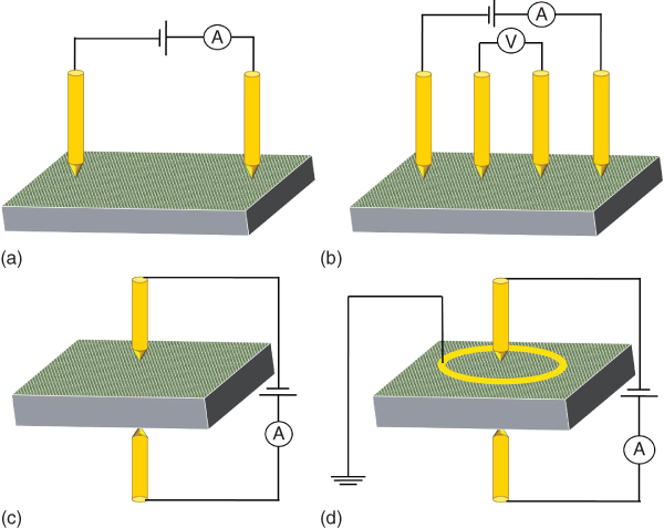
Figure 12.1 Electrical conductivity measurement configurations. (a) In‐plane two‐point. (b) In‐plane four‐point. (c) Through‐the‐thickness two‐point. (d) Through‐the‐thickness with guard electrode.
With respect to the electrode materials for two‐point and three‐point measurements, the main point is to realize an Ohmic contact, that is, a contact for which the current measured is proportional to the voltage applied over the (voltage) measuring range and a contact resistance much lower than the specimen resistance. In many cases one uses for the electrodes a noble metal (Au, Ag).
For the frequency aspect, we distinguish between direct current (DC) and alternating current (AC) measurements. In many cases for DC measurements, one employs actually a low frequency (say, 1 kHz) to avoid polarizing effects at the electrodes that interfere with the measurement. Employing a range of frequencies, typically from 1 Hz to 10 MHz, AC measurements are often addressed as electrical impedance spectroscopy (EIS). As one measures the voltage–current relation as a function of frequency, and possibly as function of and temperature, this measurement provides information about resistivity and capacity of materials. The various contributions are normally modeled employing an analog network, which tries to capture the physical mechanisms involved, for example, the contact resistance and capacitance, the material resistivity, the conductive particle contact resistance, etc.
As an example of an EIS analysis [10], Figure 12.2 shows the morphology of 1.25 vol% CB containing epoxy–amine coating on an AA2024 aluminum alloy substrate and the associated Bode plot, that is, a plot showing the absolute value |Z| and the phase angle φ of the impedance Z. Figure 12.2a shows a random distribution of the CB clusters and particles in the polymer matrix. This nice distribution was achieved by the combination of shear mixing and ultrasonication. One objective of this work was to establish a proper electrical contact between the CB clusters and the AA2024 substrate, as the presence of aluminum oxide on the alloy may lead to an increase in electrical contact resistance between the nanocomposite and the substrate.

Figure 12.2 Carbon‐black coating containing 1.25 vol% CB on an AA2024 aluminum alloy substrate. (a) TEM micrograph, scale bar = 0.2 µm. (b) Bode plot showing the absolute value of the impedance |Z| and phase angle φ as function frequency ν.
The Bode plot of the composite in Figure 12.2b shows the electrical response of this composite coating. The current response is characteristic of electrode processes under charge transfer control and reveals the existence of a CB conductive pathway in the nanocomposite. The through‐the‐thickness AC conductivity of a freestanding composite film also confirmed the existence of a CB conductive pathway in the coating. The intercept of the impedance magnitude with the y‐axis at low frequency gives a charge transfer resistance in the range of 107 Ω cm2. Since the AC electrical conductivity of a freestanding nanocomposite film at 10 mHz is 3.4 × 10⁻⁶ S cm−1, this reveals a low interfacial Ohmic drop. The result confirms not only the presence of CB percolation pathways in the composite but also the existence of a nearly Ohmic electrical contact between the AA2024 substrate and the composite coating.
Obviously, these techniques are not only used for coatings but also for bulk materials. For further technical details, we refer to Chapter 5 of [11] for a brief review, while the monograph by Barsoukov and Ross Macdonald provides an extensive discussion on impedance spectroscopy [12].
12.3 Intrinsically Conductive Polymers
In a molecule, atomic orbitals form bonding and antibonding molecular orbitals, as many as the number of atomic orbitals considered. The electrons occupy the bonding orbitals, while the antibonding orbitals are empty. For a crystalline solid, we have many interacting orbitals that do form bands, delocalized over the lattice. The highest occupied band is called the valence band, while the lowest nonoccupied band is denoted as the conduction band, as the valence band provides the bonding and excited electrons entering the conduction band can move and therefore lead to conductivity. The gap between the highest occupied molecular orbital (HOMO) of the valence band and lowest unoccupied molecular orbital (LUMO) of the conduction band is called the band gap.
The structure of the band and its filling with electrons determine the electrical behavior of a material. For a band partially filled with electrons, be it a single band or overlapping bands, applying an electric field suffices to transfer electrons from filled to empty states within the same band or the overlapping band, inducing a flow of charge. Hence a material with a partially filled band (metal) or overlapping bands (semimetal) is highly conductive with a conductivity only slightly dependent on temperature (in fact, the conductivity decreases somewhat due to increasing scattering of the charge carriers with increasing temperature, leading to a somewhat lower mobility). For a full band, however, flow of charge is impossible as empty states are not available, and for every electron moving in one direction, there is another moving in the opposite direction. Semiconductors and insulators are materials with a band gap. For insulators, the band gap is large (as compared with kT at room temperature) so that excitation of the charge carriers is only possible at elevated temperature. Semiconductors come in two types. The first type has a small band gap (as compared with kT), so that excitation of an electron from the valence band to the conduction band is possible at room temperature, thereby providing conductivity. In this process also a hole, that is, an electron vacancy with charge +|e|, is created in the valence band. The second type has a wider gap but has, provided via doping, either (occupied) electron‐donating states in the band gap just below the conduction band from which electrons can be excited to the conduction band (donor‐type or n‐type semiconductors) or (empty) acceptor states just above the valence band to which electrons from the valence band can be excited (acceptor‐type or p‐type semiconductors). In both cases the concentration of charge carriers is thermally activated showing an Arrhenius type of behavior, and this thermal activation limits the conductivity when applying a field. For all materials described briefly above, the energy level to which the electrons fill the various states is called the Fermi level, labeled as EF. For metals the Fermi level is positioned in the partially filled band, while for insulators it is located in the gap between the valence and conduction band.
The conduction mechanism for intrinsically conductive polymers is based on the presence of conjugated double bonds, in which the π‐system provides the conductive pathway through the molecule. For ethylene in a simple molecular orbital picture, two atomic p‐orbitals of the carbon atoms provide a π‐bonding (occupied) and a π‐antibonding (nonoccupied) molecular orbital with a gap in between. The interaction between these p‐orbitals is characterized by the transfer (or resonance) integral β. For butadiene, four atomic carbon p‐orbitals provide two bonding and two antibonding orbitals for which the gap between them is smaller than for ethylene. Further increasing the chain length leads to the prototype conductive polymer, trans‐polyacetylene (t‐PAc) (Figure 12.3). In this process the number of molecular orbitals increases and again leads to a valence and a conduction band. More important, the band gap decreases as well. In the limit of an infinite chain, this simple theory predicts that the band gap becomes zero and thus that polyacetylene becomes metallic.
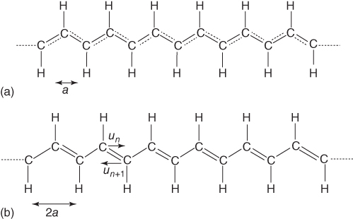
Figure 12.3 The molecular structure of trans‐polyacetylene. (a) Regular or equal bond length structure. (b) Distorted or alternating bond length structure for which the displacement from the average bond length is given by un = (−1)nu.
In reality, t‐PAc is a semiconductor. In the simple picture sketched above, we implicitly assumed that the conjugated bonds all have the same length, so that the orbital overlaps and therefore the transfer integrals β between them all have the same value. Experimentally it appears, however, that the bond lengths in a conjugated polyene chain are alternating and have a slightly different length, about 0.07–0.08 Å, the short bonds being shortened with a certain amount u and the long bonds being lengthened by u. This leads to a repeat unit value change of about 0.03–0.04 Å. Assuming that the transfer integral depends linearly on distance, for the short and long bonds, this leads to, respectively, β− = β − 2γu and β+ = β + 2γu with β the value for the average bond length and γ the coupling constant. This difference in β leads to a band gap, and therefore the electronic energy can become lower. Of course, there is a penalty (is not there always?), and in this case the penalty is coming from the σ‐bonds, who demand some energy if extended or compressed. Initially, we neglected that as all bonds had the same length. If the length is allowed to be different, we can consider the σ‐bonds as simple springs and elastic energy is involved. For small length differences, the total energy appears to be still lower and leads indeed to bond length alternation. The consequence of this intrinsic band gap is that t‐PAc is a semiconductor. For (infinite chain length) t‐PAc, the band gap is about 1.4 eV.
Similar to t‐PAc (Figure 12.4a), conjugation occurs also with cis‐PAc (Figure 12.4b) and with other units, such as phenylene (Figure 12.4c), pyrrole (Figure 12.4d), and thiophene monomers (Figure 12.4e). Many other monomers are used as well [13].

Figure 12.4 Intrinsically conductive polymers. (a) trans‐Polyacetylene (t‐PAc). (b) cis‐Polyacetylene (c‐PAc). (c) Poly(para‐phenylene) (p‐PP). (d) Polypyrrole (PPy). (e) Polythiophene (PTh).
In Sections 12.3.2-12.3.4, a more quantitative discussion is given, but we first briefly discuss in Section 12.3.1 some basics of conductivity theory, limiting ourselves to electronic conduction, thereby omitting ionic conduction. Extensive reviews, but focusing on inorganic materials, can be found in the books by Mott [14], while Blythe and Bloor discuss both the dielectric and conductivity behavior of polymers [15].
12.3.1 Some Conductivity Theory
The electrical conductivity σ of materials covers a wide range. For insulators typically σ < 10−12 Ω−1 m−1, while semiconductors cover the range from about 10−12 to 10 Ω−1 m−1 and for semimetals and metals σ > 10 Ω−1 m−1, reaching values of up to σ ≈ 108 Ω−1 m−1. For t‐PAc, σ ≈ 106 Ω−1 m−1.
The conductivity σ is codetermined by the mobility μ and density n of the free charge carriers with charge q and reads
The mobility is the drift (average) velocity 〈v〉 of the charge carriers per unit field strength with which the charge carriers move under the influence of an applied field E and has dimension (m2 V−1 s−1). In a simple model, the free motion of the charge carriers is hindered by scattering events, such as with other charge carriers or impurities, and the mobility μ is determined by the average time between scattering events τ. The force qE on the mass m of the charge carrier determines μ via
Both electrons and holes may contribute in which case q is the elementary charge e. Conductivity theory tries to explain the various contributions to n and μ, and in the sequel we briefly discuss both.
With respect to the mass of the charge carrier, in practice it does not equal its physical value, and an effective mass m* is introduced. We consider that in an applied field E the acceleration dv/dt of an electron with wave vector k is given quasiclassically by

Because the energy gain dU of the electron from the field is
substitution of dk/dt in dv/dt leads to
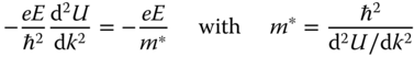
Because for free electrons U = ℏ2k2/2m, m* = m. For a band model this is no longer true and m* ≠ m, as we will see in Section 12.3.2.
The mobility μ = qτ/m is codetermined by the time τ, considered to be the time that charge carriers can move without hindrance between scattering events. In some cases the transport of charge may be hampered by traps that capture the charge carriers. If these traps have a potential well depth Utrap comparable with kT, the carriers will escape easily, and this process leads only to a reduction of the overall mobility, given by μtrap = μ[τcar/(τcar + τtrap)], where μ is the mobility between the traps and τcar and τtrap are the mean lifetime between the traps and mean residence time in the traps, respectively. This leads to a thermally activated trap lifetime τtrap ∼ exp(Utrap/kT). If there are many traps, space‐charge effects arise and the current density i ∼ V2/d3, where V is the applied voltage and d the sample thickness [16]. In this regime, interpretation is less straightforward.
So far, we assumed that the presence of free charge carriers had no effect on the lattice, but in reality there is always some distortion near an uncompensated charge. For polymers this effect is particularly strong if the material has a narrow band, implying a high effective mass and low velocity, or if the charge carrier is trapped. In these situations the lattice around the charge carrier becomes polarized, and the carrier and lattice distortion move simultaneously through the lattice. This distortion can be seen as a (pseudo)particle and is called a polaron.
In a simple model, consider the interaction of an electron with two atoms [17]. Using the internal coordinate x, describing the displacement of the two atoms from their equilibrium position, the elastic energy is Ax2. The electron will add an extra term −Bx, so that the total energy has a minimum when d(Ax2 − Bx)/dx = 0, or xmin = B/2A. At this minimum the elastic energy increased by Axmin2 = ![]() Bxmin, while the electron energy decreased by −Bxmin, so that the overall reduction is
Bxmin, while the electron energy decreased by −Bxmin, so that the overall reduction is ![]() Bxmin. Thus the electron produces a well, which will, in principle, always contain one localized state. This state becomes a bound state in which the electron is self‐trapped for a well with depth V0 and width a when m*V0a2/ℏ2 > 1. If a is approximately equal to the lattice constant, the polaron is a so‐called small polaron, characteristic of a strongly localized state, while if a equals several lattice constants, we speak of a large polaron. The latter has properties in between that of a small polaron and an unperturbed electron.
Bxmin. Thus the electron produces a well, which will, in principle, always contain one localized state. This state becomes a bound state in which the electron is self‐trapped for a well with depth V0 and width a when m*V0a2/ℏ2 > 1. If a is approximately equal to the lattice constant, the polaron is a so‐called small polaron, characteristic of a strongly localized state, while if a equals several lattice constants, we speak of a large polaron. The latter has properties in between that of a small polaron and an unperturbed electron.
In Section 12.3.2 we describe band theory in some detail, explaining why intrinsically conductive polymers, in particular t‐PAc, are semiconductors. Thereafter, we discuss some effects influencing conductivity, relevant for all intrinsically conductive polymers.
12.3.2 Simple Band Theory
For the description of the conductivity along polymer chains, a simple band picture, based on the tight‐binding approximation, is useful. This approximation applies as long as the energy perturbations due to chemical bonding are small as compared with the atomic level spacing; it ignores the electron–electron interaction explicitly but takes this effect into account implicitly via the choice of its parameters. The description uses a unit lattice cell containing one or more atoms, each with one or more atomic orbitals to characterize each atom. The band model cannot describe charge transport if the band width becomes too small with a mean free path length of the electrons equal to the lattice constant. Also if the charge carriers become self‐trapped as small polarons, the concentration of impurities and traps is high, the crystalline order is disturbed too much, or by a combination of these factors, the band description fails. In that case we need to describe charge transport by hopping, briefly discussed in Section 12.3.4.
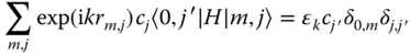
We assume that N atoms are located in a one‐dimensional (1D) lattice at positions …, –2a, –a, 0, a, 2a, …, or, generally at rm, where a is the lattice constant. The atoms are described by a single atomic wave function, given by …, |–2a〉, |–a〉, |0〉 , |a〉 , |2a〉, …, or, generally by |m〉, where the Dirac notation is used (for the intricacies, see [18]). As all atoms are equivalent, Bloch's theorem applies, and we write, for periodic boundary conditions using the allowable wave vector k = 2πj/Na with −N/2 ≤ j ≤ N/2,
where the atomic wave functions |m〉 are assumed to be known by the solution of the atomic Schrödinger equation
with H the Hamilton operator for the energy and ε the energy eigenvalue and for which 〈m|m′〉 = δm,m′ applies with δ the Kronecker delta (δkl = 1 if k = l and δkl = 0 if k ≠ l). Now we want to calculate the expectation value of a quantity represented by the operator X, say, 〈k′|X|k″〉, but as all atoms are equivalent calculating 〈0|X|k〉 suffices. For this expectation value we have
For the LHS we may write
while for the RHS we have
Now we take into account only the on‐site (k″ = k′, where k″ and k′ indicate two k‐values) and nearest‐neighbor interactions (k″ = k′ ± 1) and thus apply the Hückel approximations, reading
This simplifies the solution tremendously and we are left with

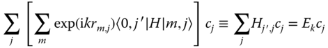
describing two band of energy levels centered at ±α with respect to EF and having a width 4β (Figure 12.5). An extended view of the band structure, showing the effect of increasing coupling, is given in Figure 12.6.
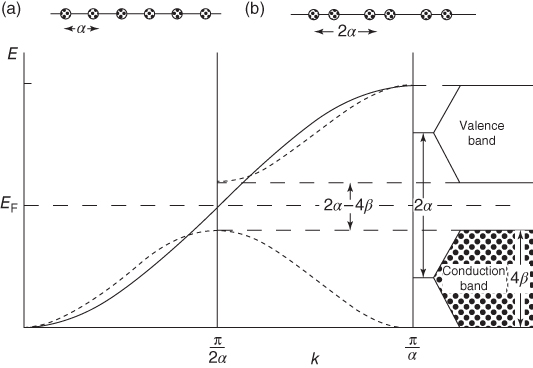
Figure 12.5 Band scheme where EF indicates the Fermi level. (a) A single band when using one atomic wave function per atom (full line in the scheme). (b) Two bands when using two atomic wave functions per atom (dotted lines in the scheme).
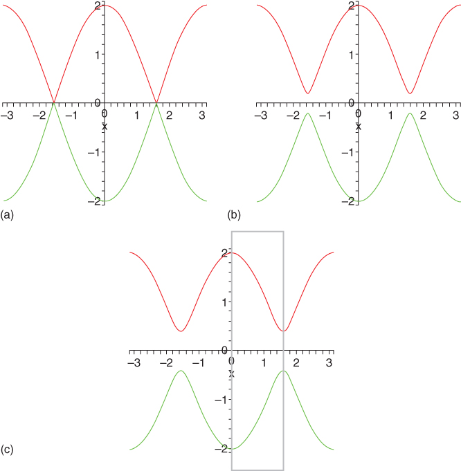
Figure 12.6 Band structure for trans‐polyacetylene showing (εk − α)/β = f(k;γ) where k is the wave vector and γ the coupling constant. The upper curve represents the conduction band, while the lower curve represents the valence band. Conventionally band diagrams, for example, as given in Figure 12.7, typically show only the part as indicated by the box in (c). (a) γ = 0.0β; (b) γ = 0.1β; (c) γ = 0.3β.
Let us return to the effective mass for a moment. Generally, for an electron in a band, the effective mass m* = ℏ2/(d2ε/dk2) for k ≅ 0 can be estimated by expanding the cosine in ε = α + 2β cos ka to second order, yielding m* = ℏ2/2βa2. Hence, the larger β, the smaller m*, reflecting the interaction among a set of atomic orbitals. When β → 0, the band becomes flat, the electron becomes localized, and m* → ∞.
The next step is to allow for more than one atom per cell. In the basic equation
the index m for a cell is just a label, and we add to it the label for atom j, so that |m〉 becomes |m, j〉, and adding a coefficient cj to be able to conserve normalization,

We have 〈k,i|l,j〉 = δk,lδi,j with δ again the Kronecker delta. The basic equation for the expectation value for the energy operator H then reads
which we can transform via
to
where ![]() . A solution is found when the determinant is zero, that is,
. A solution is found when the determinant is zero, that is,
It appears that in this case the bands are separated by an amount depending on the values for the on‐site integrals α1 and α2 of atom 1 and 2 and on the values of β involved. Note that we can play the relabeling trick again, if we realize that m, j is also just a label to which we can add the label α in case we require more than one orbital at atom j, so that |m, j〉 becomes |m, j,α〉. This will lead to more bands than just a valence and conduction band. For details we refer to the literature, for example, the very readable introduction by Sutton [18].
As an example, let us apply the above to the important example of t‐PAc for which we take alternating bond lengths (Figure 12.3b) with un = (−1)nu [19]. Using the Hückel approximations, α1 = α2 = α and indicating the transfer integrals for the short and long bonds by β− = β − 2γu and β+ = β + 2γu, respectively, with u = ![]() (un+1 − un) the displacement from the average bond length, we obtain
(un+1 − un) the displacement from the average bond length, we obtain

or, taking the real part and using z = 2γu/β,
In Figure 12.6 this solution is plotted as a function of k for various values of γ, showing an increasing band gap with increasing value of γ. The band gap at k = π/2a is 2Δ = 8γu = 4zβ. In Figure 12.7 the results of a more sophisticated band structure calculation for t‐PAc with identical and alternating bond lengths are plotted. Here several wave functions per atom are taken into account. This figure shows not only the absence and presence of a band gap for the symmetric and distorted structure, respectively, but also a rather similar band structure for the rest of the bands [20].

Figure 12.7 Band structure for t‐PAc using five atomic wave functions per atom so that five valence and five conduction bands result. The dotted line indicates the Fermi level. The symbols at the x‐axis indicate the direction in the unit cell in k‐space, the so‐called Brillouin zone. (a) For identical bond lengths (1.4 Å) showing the absence of a band gap. (b) For alternating bond lengths with experimental bond length values (1.36 and 1.43 Å) showing the presence of a band gap. (c) For alternating bond lengths with exaggerated bond length difference (1.34 and 1.54 Å) showing an increased band gap.
The total electronic energy is given by Uelec = −2∑kεk, where the sum runs over the occupied levels. In view of the density of levels the sum can be replaced by an integral via Σk(·) → (L/π)∫(·)dk = (Na/π)∫(·)dk, so that
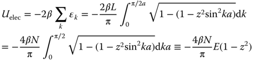
For z ≪ 1, the elliptic integral of the second kind E(1 − z2) can be approximated by

Now we have to realize that the σ‐bonds are also distorted, which leads to a distortion energy, approximated as an elastic energy reading Uelas = ![]() K∑n(un+1 − un)2, where K is the force constant. The total energy thus becomes
K∑n(un+1 − un)2, where K is the force constant. The total energy thus becomes
Realizing that z = 2γu/β and minimizing U via dU/du = 0, we obtain a saddle point at u = 0 and two stable minima at u0/a = ±4 exp[−(1 + 1/2λ)], where the dimensionless electron–phonon constant λ = 2γ2/πKβ is introduced. Hence, the band gap becomes 2Δ = 4zβ = 16β exp[−(1 + 1/2λ)]. Using K = 21 eV Å−2, as relevant for t‐PAc, and requiring that 2Δ for the ground state leads to 1.4 eV, the optimum occurs for 2γ/β = 1.65 Å and u0 = 0.042 Å, the latter corresponding to a bond length increase of 31/2u0 = 0.073 Å. Altogether the energy decrease per atom for the dimerized state as compared with the equal bond length state is ΔU/N ≅ 0.015 eV. Hence, the structure with alternating bond lengths is indeed favored. In Figure 12.8a the total energy is plotted, showing a double minimum energy well, as for any two consecutive bonds either bond could be shortened (and the other lengthened), and, hence, the ground state is doubly degenerate with configurations I and II. The model is often referred to as the Su–Schrieffer–Heeger (SSH) model, although in fact in 1955 Peierls already predicted the splitting of such a partially filled band for a linear chain (linear metal) using rather general arguments [21].
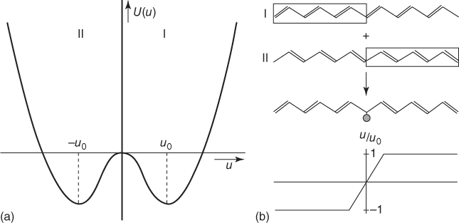
Figure 12.8 (a) Total energy for trans‐polyacetylene as a function of u showing a double well, favoring the alternating bond length structure. (b) Schematic of a soliton.
There is one more issue to consider for t‐PAc that is related to the degeneracy of its ground state, as characterized by the bond alternation parameter u/u0 with values ±1. If two parts of the chain for some reason or another have a different bond alternation parameter, for example, due to substitution at a chain end, a defect will occur where u/u0 changes sign (Figure 12.8b). This defect contains an unpaired electron residing at a carbon atom having two long (single) bonds, although the chain as a whole is neutral. The deviation from the regular long–short pattern is extending over several lattice spacings of size a, and for a defect centered at n0, it can be described by un = u tanh[(n−n0)/ξ] cos nπ with ξ the characteristic length. Such a defect is called a soliton. Actually for t‐PAc, ξ ≅ 7a, implying that it takes about 14a before u/u0 has changed its value from −1 to +1. Since the energy of the chain on both sides of the defect is equal, a soliton can easily move along the chain with an activation energy estimated as 0.04 meV (≅0.0016kT at 25 °C). In contrast, if the soliton would be localized on one atom, the activation energy would be about 40 meV (≅1.6kT at 25 °C). For t‐PAc, in the band picture sketched above, for a soliton, m* ≅ 6m. This relatively low value of the effective mass is directly related to the small value for u0 as compared with a. The formation energy of a soliton for t‐PAc is estimated to be 0.6Δ, and since the experimental band gap of t‐PAc is ≅1.4 eV, the formation energy is ≅0.42 eV. Hence, solitons are not created thermally, and their presence rests on external factors, such as substitution. The soliton in a broader context has been reviewed by Scott, Chu, and McLaughlin [22].
12.3.3 Doping
As the electron associated with a soliton is nonbonding, a soliton is a zero energy state of the chain with its energy level lying at the center of the band gap, and its wave function can be considered to consist of an equal contribution of states at the edges of the valence and conduction band (Figure 12.9a,b). The model is said to be charge conjugate invariant since the results are independent of the type of charge carrier (electron or hole). When an electron‐donating group is attached to the chain, that is, t‐PAc is doped, a negatively charged soliton can be created with energy less than an excited electron in the conduction band. Similarly, for electron‐accepting groups a positively charged soliton can be created, needing less energy than a hole in the valence band (Figure 12.9c,d). Consequently, we can have:
- Singly occupied solitons with charge zero but spin
 (or −
(or − for an antisoliton).
 - Doubly occupied solitons with charge −e and spin 0.
- Nonoccupied solitons with charge +e and spin 0.
Figure 12.9 Energy levels in t‐PAc for solitons and polarons. (a) Soliton. (b) Antisoliton. (c) Negative soliton. (d) Positive soliton. (e) Negative polaron. (f) Positive polaron.
As discussed in Section 12.3.1, a charged defect can form a polaron, and also a charged soliton can do so. When a neutral soliton and a charged soliton interact, their degenerate levels can form two separated levels, like a bonding and antibonding orbital. Dependent on whether the charged soliton is negatively or positively charged, the new configuration is described as a negative or positive polaron, respectively (Figure 12.9e,f).
In a theoretical description using periodic boundary conditions, the presence of solitons depends on whether the chain contains an odd or even number of atoms. As the chain end is connected to the chain beginning, both sides must have a different type of bond. This condition is fulfilled for an even number of atoms but not for an odd number. Hence, for an odd number of atoms, a periodic chain should contain at least one soliton. For an even number of carbon atoms, the chain contains obviously either no solitons or a soliton and antisoliton.
In summary, in this model doping of t‐PAc occurs via solitons, either initially present or created as a soliton/antisoliton pair. With increasing dopant levels, polarons are formed, and the soliton states broaden into a band that eventually overlaps with the valence and conduction bands, leading to a metallic state. To illustrate the effect of doping, Figure 12.10 shows the tremendous change in conductivity for t‐PAc, oxidized via exposing to halogens, like Cl2, Br2, or I2, or a gas like AsF5 [23]. This will lead to a polymer salt, such as (CH+(I3−)0.1)x for 10 mol% iodine doping.
Figure 12.10 The effect of doping on the conductivity of t‐PAc.
The model for t‐PAc used so far takes the deformation of the lattice into account but neglects electron–electron interaction, at least explicitly. The other extreme is to neglect the electron–lattice interaction (that is, to start with an equal bond model) but take the electron–electron interaction explicitly into account. This destroys the charge conjugation invariance and leads also to a band gap. We do not discuss that model here any further and refer to the literature [24]. In fact, for a detailed description both effects have to be taken into account, as already discussed by Salem in 1966 [25]. Another aspect that is important is the conjugation length. So far, we considered the chains as being straight. In reality this is not the case. Two models are in use to describe this. The first is the Kuhn model, in which a long chain is divided in straight parts of varying length. In this case, conjugation is maintained in every straight part. However, the local kinks in the chain have a high energy. Therefore a second model, the wormlike chain model, is considered in which a gradual deformation along the chain occurs. Here the concept of conjugation length is less clear, although eventually the deformation will destroy the conjugation.
Apart from the molecular characteristics, also the morphology plays a rather important role. Charge transfer from one molecule to another is obviously facilitated by larger chain–chain overlap, so that a material with aligned chains has a larger mobility and therefore larger conductivity. While doping can increase the electron conductivity by 5–10 orders of magnitude, aligning can lead to another 2 decades increase. These effects are illustrated for a particular example in Section 12.4, although generally the relationship is by far not so straightforward as suggested by the overlap argument.
For most other conjugated polymers, for example, for those shown in Figure 12.4, the situation is different from that for t‐PAc, because they usually do not have a degenerate ground state. Hence, in these materials solitons are not formed because such an extended defect is energetically unfavorable. It is possible, though, to form polarons, as in that case the deformation is localized and has a relatively small distortion energy. In these materials, doping usually occurs via acceptor doping with positive polarons as a result. With increasing dopant level, the polaron states start to interact and form bands that eventually overlap with the valence and conduction bands, again leading to a metallic state.
12.3.4 Hopping
The charge transport mechanism within a chain being discussed, we now turn our attention to the charge transport between chains, as this codetermines the overall conductivity. This is usually described by hopping, a mechanism that is also important for conductive particulate composites. Hopping may also occur if a band description no longer applies and mainly localized states exist as in a single conjugated molecule and in amorphous materials.
In all these cases, charge transfer can occur by moving an electron from one localized state to another. Hopping refers to transfer over a barrier, while tunneling refers to transfer through the barrier. In principle, both mechanisms can occur (also simultaneously). For the former, the electron must acquire sufficient thermal energy to overcome the barrier, while for the latter the separation between localized states must be small enough for the wave function to extend through the barrier (Figure 12.11a). In most cases, one does not discriminate between these two mechanisms. With increasing amount of disorder, the levels associated with localized states spread out into the energy region that would be the band gap for a regular lattice. Since the hopping mobility decreases rapidly with hopping distance, the mobility in this region is small and a mobility gap (Figure 12.11b) exists, even though the density of states is not zero.

Figure 12.11 Disordered semiconductor conductivity. (a) Charge transfer via hopping and tunneling. (b) Band structure and the associated mobility gap.
The simplest approximation to such a situation is to use still the tight‐binding approximation but with a potential having random depths [26]. For a potential depth distribution width ΔV comparable with the band width 2β, the mean free path is approximately equal to the lattice spacing. In this case the wave function |Ψ〉 contains a random phase factor exp(iφn), as the electron is unable to imprint its phase on the next site. Moreover, it contains a localization factor exp[−(r − r0)/ζ], in which the localization length ζ is infinite at the onset of localization but decreases as ΔV increases, so that eventually electrons are localized at position r0. Altogether we have for the wave function
For finite length chains (oligomers), the π‐electrons, though mobile within the molecule, are obviously localized on the molecule. In this case one can use the quasi‐band structure, that is, a distribution of molecular orbital levels discretely along the dispersion curve of the infinite polymer [27]. Moreover, these molecules are usually far from perfect, which also leads to localized states. Consequently, charge transfer is dominated by hopping of charge carriers from one localized state to another.
So, there are two complementary approaches to describe the conductivity in amorphous semiconductors. In the band picture the charge carrier concentration is low but strongly temperature dependent because of the thermal activation of the electron across the gap, while the mobility is high and weakly temperature dependent. In the polaron picture the converse is true. The charge carrier concentration can be high and temperature independent since every site can form a polaron, but the mobility is low and thermally activated. In the adiabatic regime the vibrational motion of the atoms is slow as compared with that of the electrons, and electrons adjust instantaneously to the atomic positions.
In a simple model [28] for hopping, one considers two localized states, a filled one at or slightly above the Fermi level and the other one empty and above the Fermi level. Their spatial and energy separation are R and ΔE, respectively. The hopping rate χ is determined by three factors. As the two states have a different k‐value, a phonon is required, and the first factor is the probability for the phonon involved to have the energy ΔE, given by the Boltzmann factor exp(−ΔE/kT). The second factor is the probability of electron transfer. If a state is exponentially localized, that is, its wave has a tail exp(−r/ζ), the tunneling probability is given by exp(−2R/ζ). The third factor is the attempt frequency ν0, dependent on the electron–phonon coupling constant γ and the phonon density of states. Hence, χ = ν0 exp(−2R/ζ) exp(−ΔE/kT).
For the mobility we use the Einstein relation μ = eD/kT relating the mobility μ to the diffusion coefficient D, where the simple expression D = χR2/6 for random diffusion is used. For the charge carrier concentration, we use n = kTρ(EF), where ρ(EF) is the electronic density of states at the Fermi level. Hence, the conductivity σ becomes

One would expect that only the nearest neighbors participate in hopping. However, with increasing range and considering more remote neighbors, the probability for finding a low barrier increases, although the overlap between wave functions decreases. Hence, Mott argued that the exponent h = −2R/ζ−ΔE/kT should be optimal or that dh/dR = 0. As at least one state should be available at given R and ΔE, we also have 1 = (4π/3)R3ρ (EF)ΔE. After some calculation this leads to
so that the conductivity becomes

The numerical constants should not be taken too literally, and typically the value for σ0 is too high. Experimentally, the dependence is often observed to be T−m with ![]() < m <
< m < ![]() rather than T−1/4. The model is often addressed as variable‐range hopping, as its range of hopping depends on temperature.
rather than T−1/4. The model is often addressed as variable‐range hopping, as its range of hopping depends on temperature.
12.4 An Example: P3HT/PCBM Photovoltaics
The literature on the applications of intrinsically conductive polymers is large. These materials are, for example, applied in photovoltaics (related to photoinjection of charge carriers), sensing (related to changing doping characteristics upon exposure to gases), and electronics (e.g. field effect transistors). Here we provide only one example of materials, as used in photovoltaic applications. This example not only illustrates the morphological complexity of intrinsically conductive polymers but also the use of sophisticated characterization techniques [29]. For the many other applications, we refer to the books indicated in “Further Reading,” for example, by Barford or Wan.
Poly(3‐hexylthiophene) (P3HT) has become one of the most used components in organic electronics [30], often in combination with (6,6)‐phenyl‐C61‐butyric acid methyl ester (PCBM). P3HT is a conjugated polymer that has a tendency to aggregate via π–π stacking of the conjugated backbone [31, 32]. This is often beneficial for the performance of electronic devices, because the ordering is known to increase the hole mobility and to result in a more phase‐separated morphology, which can lead to better performing devices [33]. Although in the field of organic photovoltaics more efficient donor–acceptor combinations have been developed [34] and there are nowadays many high performance polymers available, some even surpassing the 10% power conversion efficiency [35], P3HT as a component in the P3HT/PCBM solar cells remains a cost‐effective choice in large‐scale production [36]. Such cost‐effective manufacturing of bulk‐heterojunction solar cells relies on printing technology. In this case, the device performance depends on a long list of processing conditions, one of them being the ink used, possibly containing preformed nanostructures. Therefore reliable ways are needed to characterize these inks, which are often based on (halogenated) organic solvents, and the layers deposited with them. For further information on organic photovoltaics, we refer to [37, 38].
One of the most revealing characterization techniques as a means to characterize P3HT assemblies in solution is cryo‐TEM, coupled with tomography (see Section 8.10.1). The assemblies to be discussed here were made by first dissolving P3HT at higher temperature and subsequently cooling the solutions to induce the thermochromic phase transition [39, 40]. Both toluene, a nonhalogated solvent, and 1,2‐dichlorobenzene (oDCB), a halogenated solvent, were used to illustrate the potential of cryo‐TEM for the general purpose of characterizing photovoltaic inks. A P3HT concentration of 1 wt%, representative for solution processing of organic electronic devices, was used.
In Figure 12.12a, a cryo‐electron tomography‐derived segmentation of the lamellar stacks is shown [29]. The regions corresponding to the low intensity regions in the tomographic reconstruction scatter the strongest and represent the lamellae. The background and the aliphatic regions are transparent. Analysis of a smaller volume from the middle of the nanowire (Figure 12.12b) shows a more pronounced order, that is, a clear periodicity in lamellar stacking with a 1.7 nm stacking. The bulk of the nanowire is made up from π–π stacked regions that form the lamellae alternating with aliphatic regions.
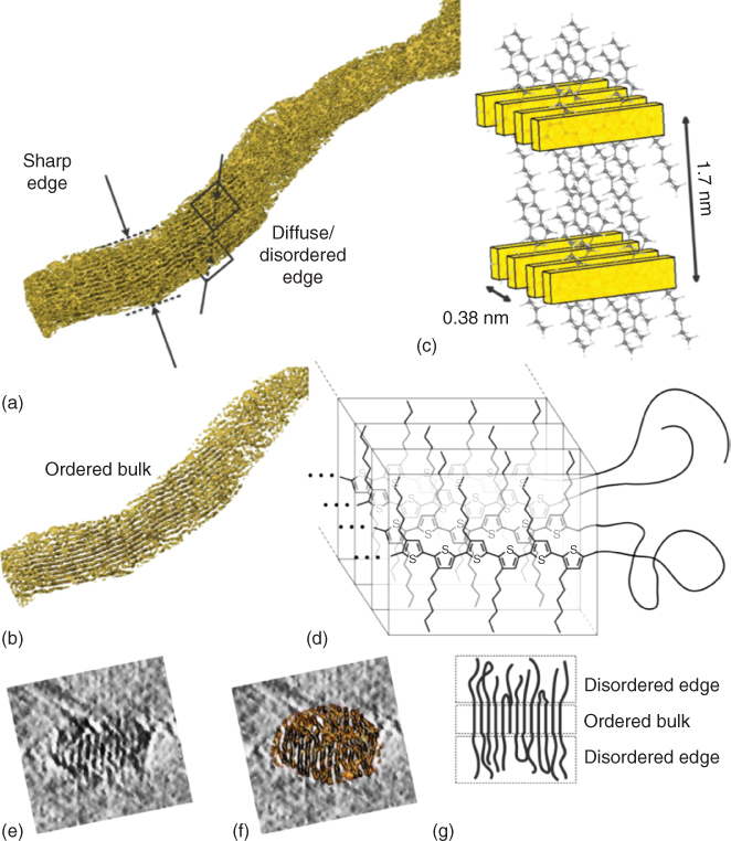
Figure 12.12 P3HT characteristics. (a) Isosurface generated from tomographic reconstruction of a P3HT nanowire. (b) Isosurface from the middle of the nanowire showing increased order. (c) Model of the lamellar order in the middle of the nanowire. (d) Model showing crystalline order in the bulk and disorder on the side of the nanowire. (e) Slice from the tomographic reconstruction showing a cross section of the wire. (f) The same slice overlaid with the corresponding segment of the segmented structure. (g) Cartoon depicting the ordered bulk and the disordered edges.
A combination of the findings with the crystal structure of phase I P3HT is depicted in Figure 12.12c [41], in which the conjugated polymer backbones are highlighted. The planes with a direction parallel to the polymer chain are referred to as the sides of the nanowire and the planes in the direction perpendicular to the lamellar stacks as the top and bottom. The tomographic model shows a sharp edge for the top and bottom of the nanowire and diffuse edges for the sides of the nanowire. In addition it shows more order in the bulk than toward the sides of the nanowire, which is in consonance with the diffuse edges. The top and bottom of the nanowire are bordered by lamellae, giving rise to this sharper edge, while on the sides the polymer chains are branching out and possibly folding back, giving rise to a more diffuse edge, as illustrated by the molecular model shown in Figure 12.12d. The morphology of this P3HT nanowire in solution can be considered to be a highly ordered stack of lamellae that slowly branches out toward the sides, giving rise to more disorder. To provide an impression of the quality of the raw reconstruction, a slice of a cross section of the reconstruction is shown in Figure 12.12e, which is overlaid with the corresponding original segment of the segmented structure in Figure 12.12f. Because not enough resolution is present to visualize individual polymer chains, it appeared to be impossible to segment the disordered parts clearly. However, it was concluded from the increasing disorder toward the outer parts of the cross section that the wires are more ordered in the bulk and more disordered at the edges, as illustrated in the cartoon in Figure 12.12g.
The obtained insight in the anisotropy of the P3HT wires resulting from their crystal structure is important to understand the function of P3HT assemblies in organic electronic devices in terms of charge percolation, conductivity, electronic landscape, and morphology.
Further characterization of P3HT in combination with PCBM as used in photovoltaic coatings in organic solar cells was also reported [42]. The performance depends strongly on the nanoscale morphology of the active layer, which is typically a bulk heterojunction of an electron donor and acceptor phase with ideally an optimized balance between a large interface area for exciton dissociation and phase continuity for charge percolation [43]. Also the crystallinity of the different phases is of importance as charge carrier mobility is directly related to the degree of order in these layers [44]. Ordering in such devices strongly depends on the processing method and further postprocessing treatments such as thermal annealing, slow drying, or solvent/vapor treatment [32]. However, postprocessing treatments are cumbersome for the manufacturing process. Annealing is not compatible with the commonly used PET and PEN flexible substrates that have a glass transition temperature of 70 and 120 °C, respectively [45]. Solvent annealing and controlled drying methods prevent rapid manufacturing and are hard to control. Therefore these postprocessing treatments are not suitable for cost‐effective large‐scale production.
The use of regioregular P3HT as electron donor and PCBM as the electron acceptor provides reliable solar cells under a wide variety of processing conditions [30]. As stated before, P3HT can form well‐defined highly crystalline nanowires in solution, for example, through modulation of the solvent quality, temperature, or using templated assembly [46–48]. Devices processed from the resulting dispersions display an increased power conversion efficiency as compared with nonprestructured devices, as a consequence of the presence of a highly crystalline, nanostructured network [49, 50]. It is therefore of interest to consider growing crystalline nanostructures in solution and to make an ink from the resulting dispersion. Subsequently the ink can be processed directly to create an optimal morphology, thereby decoupling nanostructure formation and device fabrication, so that the latter no longer depends on the deposition process. Achieving control over crystallization may further provide access to new morphologies that would be difficult or impossible to create by posttreatments due to the limited conformational mobility of the polymers in the photoactive layers.
As shown in Figure 12.13a–c, structure evolution occurs in the photoactive layers, similar as observed in the solutions/dispersions. Because nanocrystalline PCBM in the photoactive layer is a stronger scatterer than the P3HT, P3HT is light and PCBM is dark. In the devices processed from the initial solution (Figure 12.13a), only small, fiber‐like structures of P3HT are visible, which have most likely been formed during processing, since they are not observed in cryo‐TEM for the solution. They do not have a preferential orientation and are usually curved. In the photoactive layers processed from dispersions at an intermediate state (Figure 12.13b), the same phase segregation is observed as in solution. This is manifested as lighter regions, which are P3HT rich, and darker regions, which are PCBM rich. In addition, white thin P3HT fibers can be abundantly seen, similar to the nuclei observed in cryo‐TEM for the ink. These fibers are not significantly different from the ones in Figure 12.13a, although they originated from the processing and the ones in Figure 12.13b from nucleation in solution and partly from processing.
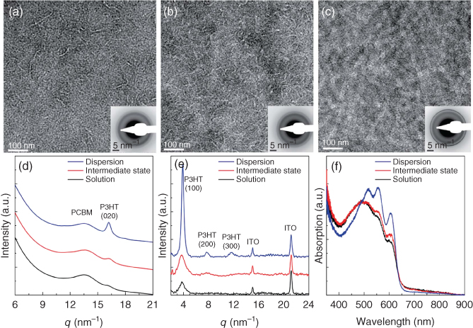
Figure 12.13 P3HT–PCBM characteristics. (a–c) TEM images of photoactive layers obtained from the initial solution, an intermediate state, and the final dispersion, respectively. The P3HT is light and PCBM dark. The insets are the LDED patterns corresponding to the images. (d) Radially integrated LDED patterns. (e) WAX diffraction patterns of the photoactive layers. (f) UV–vis absorption spectra of the photoactive layers. Note that the final PCBM has a higher density than P3HT, so that the contrast is inverted and P3HT will show up as lighter areas. In contrast, the cryo‐TEM images show P3HT as dark areas against a background of vitrified solution of PCBM in toluene.
The layers prepared from aged dispersions showed the same nanowires of about 25 nm wide and >1 µm long as observed in the cryo‐TEM images of the dispersions (Figure 12.13c). In contrast with the former fiber‐like structures, these nanowires are rigid, and their lamellae lie consistently parallel to the substrate, which can be deducted from the constant 25 nm width of the nanowires as well as from the absence of the (100) reflections in the low dose electron diffraction (LDED) patterns. Because most of the polymer phase is incorporated in the nanowires, there is no significant change in structure during processing. The radially averaged LDED pattern in Figure 12.13d demonstrates that aging of the solutions leads to an increased crystallinity of the P3HT in the corresponding layers as the P3HT peak at d = 0.39 nm (q = 16.1 nm−1) becomes sharp and high as compared with the PCBM peak at d = 0.46 nm (q = 13.6 nm−1). The same state of PCBM is observed in all the photoactive layers. Because the LDED pattern for the solution did not show the same nanocrystalline PCBM peak, the nanocrystalline PCBM in this case must have grown fast during the deposition process. Hence, nanocrystalline PCBM can grow either during processing or in solution and significantly faster than the P3HT. The increased crystallinity of P3HT was confirmed by the appearance of a strong (100) reflection at d = 1.7 nm (q = 3.7 nm−1) and the higher order reflections in the wide‐angle X‐ray (WAX) diffractograms (Figure 12.13e) of the films, as well as by the UV–vis absorption spectrum of the photoactive layers that showed an increasing red shift with increasing aging time of the used solutions (Figure 12.13f).
This study examined for the first time these systems with cryo‐TEM – not commonly used for organic solvents – in combination with LDED. Clear evidence for the decoupling of the structure and morphology formation was provided, that is, no significant additional structure formation happens during processing. Intrinsic to the crystalline structures, there is a small decrease in open circuit voltage. In contrast, the evolution in morphology from very intermixed with a few fibrillar structures to a phase‐separated network with large polymer crystals leads to a significant increase in photocurrent.
Understanding the role of morphological variations will be key to the efficient large‐scale production of polymer solar cells and also opens the road to create more innovative designs for the internal structure of such devices. Following the structure formation from the solution to the device provides valuable structural information of the materials in solution and in the devices; furthermore this structural study provides valuable information for the application of printing technology for organic solar cells. As the wires studied seem to be the most stable form of P3HT, their application as preformed structures could prevent significant morphological changes that could affect the long‐time performance of many device structures.
While the first study [29] revealed some insight in photovoltaic dispersions, the latter study [42] elucidates some of the relations between starting dispersions and the resulting photovoltaic structures, meanwhile providing an example of how cryo‐electron tomography can help to understand the connection between structures in solution and the resulting solid‐state morphology.
12.5 Conductive Composites
The basic idea of a conductive composite coating is to realize (a network of) conductive pathways in a nonconductive matrix, so that overall a conductive material is realized. The description of such particle network is often considered to be a percolation problem (Section 12.5.1), although other approaches exist (Section 12.5.2). Practically speaking, one needs conductive particles (Section 12.5.4) and a proper dispersion of the particles in the matrix.
12.5.1 A Glimpse of Percolation Theory
If we mix electrically conducting and insulating particles at random, using an increasing fraction of conducting particles, the mixture will be at first insulating; however, at a certain fraction a transition to a conductive mixture occurs. This change occurs over a small volume fraction change of conductive particles, and thereafter the conductivity still increases, albeit slowly. This phenomenon is called percolation, and the transition occurs at the percolation threshold. The phenomenon can be considered as a geometrical phase transition for which, at the percolation threshold, infinitely connected clusters of conductive particles appear. Percolation can take place on random networks but is mostly studied for regular networks. We first pay some attention to regular networks and thereafter make a few remarks about random networks.
Some of the regular lattices in use are shown in Figure 12.14. Essentially two types of percolation processes exist, namely, site and bond percolation. Where required, the type of percolation will be indicated by the superscript (b) or (s). Site percolation considers sites, and these sites are either occupied or empty. Two nearest‐neighbor sites are connected if they are both occupied. A (site) cluster is a group of such connected sites, and, given a site has probability p of being occupied, the percolation probability function P(p) is the probability that a site belongs to an infinite cluster. Bond percolation considers bonds between sites, and these bonds are either open or closed. Open in this respect means that transport can take place, that is, a bond connects sites. If at least one path consisting of only open bonds exists between two sites, these sites are said to be connected, and a set of bonds bounded by closed bonds is called a (bond) cluster. If a bond has probability p of being open, P(p) is the probability that the bond belongs to the infinite cluster linked by such open bonds. In both site and bond percolation, when the probability p approaches the percolation threshold pcri, a transition from a macroscopically disconnected state to a connected state takes place. The function P(p) = 0 for p < pcri and thereafter rises steeply until eventually P = p = 1.
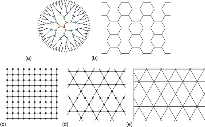
Figure 12.14 Some regular lattices. (a) Bethe lattice, z = 3. (b) Honeycomb lattice, z = 3. (c) Square lattice, z = 4. (d) Kagomé lattice, z = 4. (e) Triangular lattice, z = 6.
The value for pcri depends on whether site or bond percolation occurs and on the dimensionality of the lattice (Table 12.1). The values for pcri are usually calculated via renormalization techniques and simulations, and only for the Bethe lattice and some 2D lattices, pcri can be calculated analytically. For the Bethe lattice, for example, pcri(b) = pcri(s) = (z − 1)−1, where z is the coordination number of the lattice. One can prove that pcri(b) ≤ pcri(s) for a given lattice of particular dimensionality d. Further, pcri decreases with increasing coordination number z and, for given z, decreases with increasing d. Further, we will need the correlation length ξ, which represents for p < pcri the typical radius of a connected cluster and the length scale over which the network is macroscopically homogeneous.
Table 12.1 Percolation characteristics.
| Dimensionality | Lattice, z | pcri(b) | pcri(s) | β | μ | ν |
| 2 | Honeycomb, 3 | 0.6527 | 0.6962 | 5/36 | 1.3 | 4/3 |
| 2 | Square, 4 | 0.5000 | 0.5927 | |||
| 2 | Triangular, 6 | 0.3473 | 0.5000 | |||
| 3 | Diamond, 4 | 0.388 | 0.428 | 0.41 | 2.0 | 0.88 |
| 3 | SC, 6 | 0.2488 | 0.3116 | |||
| 3 | BCC, 8 | 0.1803 | 0.246 | |||
| 3 | FCC, 12 | 0.119 | 0.198 |
z, coordination number; the values for β, μ, and ν apply for each dimensionality.
Close to the percolation threshold, physical quantities depend on p − pcri, and for p − pcri < 1, the probability P, conductivity σ, and coherence length ξ are given by
where P = σ ≠ 0 for p > pcri and ξ ≠ 0 for p < pcri. The exponents β, μ, and ν are independent of the type of lattice and depend only on the dimensionality (Table 12.1). For bond percolation zpcri(b) ≅ d/(d−1) is accurately obeyed empirically, the significance of which is not understood. Note that for sample size L ≫ ξ, the system is macroscopically homogeneous, but for L ≪ ξ the system is inhomogeneous and the properties depend on the value of L. For example, the mass M of clusters in this regime scales as M ∼ LD, where the fractal dimension D = d − β/ν. For L ≫ ξ, D = d.
To illustrate some of the above for the conductivity, we consider when and how electrical conduction across a macroscopic region occurs, in terms of the microdetails of the packing of the particles. The approach is to renormalize, that is, to coarse‐grain or group particles together to a new, renormalized particle having the properties of the majority of particles participating in the formation of the renormalized particle. In principle, this process is iterated to obtain a solution of the relevant equations. As a concrete example, we use a 2D structure having a triangular lattice with renormalization by three particles (disks). For the original packing the microdescription is in terms of sites that are either occupied or unoccupied with a conductive particle. We denote by p the probability that any site is occupied, independent of whether any other site is occupied or not. The occupancy distribution of sites provides the exact microdescription of the system for which we only know the single site probability p.
When we increase the length scale by a factor of b, for example 31/2, we increase the area by b2 = 3, we obtain a coarse‐grained or renormalized description. At this higher level of description, here thus a cell of 3 sites, we use the majority rule and consider a cell as occupied if and only if 2 or more of the sites are occupied (Figure 12.15). Let us call p1 the probability that a cell of three sites is occupied. The probability p1 is then the sum of probabilities of four mutually exclusive states. Using p for occupied sites and (1−p) for unoccupied sites, we have once p3 and three times p2(1−p).

Figure 12.15 Percolation and renormalization by taking three spheres together applying the majority rule. (a) A schematic of the original packing. (b) Four possible renormalized sites.
The percolation threshold (critical point) occurs if the original probability p equals the renormalized probability p1. We thus have
In this particular case, the solution of this equation does not require iteration but yields directly the solutions p* = 0 and p* = 1, which represent the so‐called stable fixed points, and the solution p* = 0.5 representing the unstable fixed point. The unstable fixed point solution thus appears to be the exact solution for this 2D percolation problem, which, however, is fortuitous.
Let us now calculate the critical exponent ν, which describes the onset of the percolation phenomenon. We use the correlation length ξ for which the expression for the original packing is given by ξ = C|p − pcri|−ν, so that for the renormalized packing we have ξ1 = C|p1 − pcri|−ν with ξ1 = ξ/b. Combining results in

Expanding p1 as p1 = p* + λ*(p − p*) + ⋯ with λ* = (dp1/dp)p=p* and substitution in the original equation p1 = p3 + 3p2(1 − p) yields
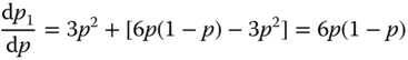
so that λ* = 3/2. Because b2 = 3, we obtain
The exact value is ν = 4/3. Approaching the threshold, the coherence length ξ of the clusters increases until ξ diverges at the threshold itself. This implies that conductive clusters span the complete system, and therefore the system becomes macroscopically conductive.
For finite 3D systems, some corrections are required. For example, Fisher [51] showed that for any property
where u = L1/ν(p − pcri) ∼ (L/ξ)1/ν, f(u) is an analytical function of u, L is the sample size, and ν is the correlation length exponent. If the relation X ∼ (p − pcri)δ near pcri and for L → ∞ applies, then one must have x = δ/ν. There is also a shift in pcri given by [52]
where pcri(∞) and pcri(L) denote the critical value for an infinite sample and of size L, respectively. In practice, for transport properties, one applies, for example [53],
so that from a range of X values, x can be estimated by fitting the results to this equation.
For coatings the thickness is the limiting factor, and for a particulate coating with particle size Rp, the effect of sample thickness is described by
where pcri(l) is the effective percolation threshold for a sample with thickness l, pcri(∞) the threshold for l → ∞, and c a constant. From experiments with layers of particles [54], it appeared that ν ≅ 0.85, in good agreement with the theoretical value ν ≅ 0.88. The finite thickness also affects the conductivity. Combining the above with σ ∼ (p − pcri)μ, one easily obtains
where σ1 (σ2) is the conductivity for a sample with thickness l1 (l2) and μ3 (μ2) the critical exponent for 3D (2D) percolation. This result is in good agreement with the data indicated before [54].
In reality, networks are hardly ever regular. Hence, it is important to consider the percolation on random networks. Distributing inclusions at random in an otherwise uniform system, it appears that for regular and random networks, the critical volume fraction φcri = pcri(s)f, where f is the packing fraction of the network, is invariant [55]. For 2D (i.e. for disks) φcri ≅ 0.45, whereas for 3D (i.e. for spheres), φcri ≅ 0.16. To illustrate this, consider a random close packing of spheres for which f ≅ 0.64, so that for a BCC lattice we calculate pcri ≅ 0.25, close to the theoretical value 0.246.
Another practical aspect is the effect of a particle size distribution. A criterion for relatively weak perturbation of the particle size [56] states that, if α(d) ≡ 2 − dνd > 0, the critical behavior can change. Here, d is the dimensionality of the system and νd the exponent for the correlation length ξ in d dimensions (Table 12.1). For 3D, νd ≅ 0.88 and thus α(3) ≅ −0.64, while for 2D, νd = 4/3 and thus α(2) = −2/3. Hence, in these cases the particle size distribution should not change the critical behavior [57]. However, several experiments do show an effect of the particle size distribution; see, for example, [58], which also provides a general review.
The application of percolation theory is wide and finds, for example, also application in the description of the structural, mechanical, and rheological properties of polymers and gels, fracture and fault patterns in heterogeneous rocks, the spread of diseases, transport of liquids through particulate and porous media, and the diffusion and growth of particles. A widely used introduction is the booklet by Stauffer and Aharoni [59], while Sahimi [57] provides an extensive overview over various applications. For a review of conductivity in relation to percolation, see [60].
12.5.2 Other Approaches
There are, however, other models to describe the conductivity of particulate composite materials. One of them is effective medium theory (EMT) [61] in which the property of a composite is determined by a combination of the properties of the components. If the composite is treated as a mixture of (conductive) spherical particles of varying sizes with volume fraction φ in a (poorly conductive) matrix (Figure 12.16a), the conductivity is described by the symmetric Bruggeman equation [62–64]
where σf, σm, and σ are the conductivities of the filler, matrix, and composite and A is a factor, A = 2 for spherical particles, determining the local field concentration at the conductive particles. The critical volume fraction φcri is related to A via A = (1 − φcri)/φcri and for spherical particles leads to φcri = 1/3. The main approximation is that all the domains are located in an equivalent mean field, but this is not the case close to the percolation threshold where the system is governed by the largest cluster of fillers, which is a fractal. Hence, the threshold value is far from the 16% expected from percolation theory and observed in experiments. However, in two dimensions, the model gives a threshold of 50% and has been proven to model percolation relatively well [65, 66]. In a generalized form of EMT [67], the conductivity is obtained from the asymmetric Bruggeman equation
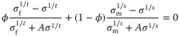
where t and s are exponents. Here both phases are effectively a mixture of the two pure components (Figure 12.16a). Using t = s = 1, we regain the symmetric Bruggeman equations. With t, s, and A as parameters, good fits to experimental data can be obtained. An extension of the model to AC measurements is available [67]. While percolation theory is particularly useful in the concentration range where the percolation transition takes place, EMTs are more useful for high concentrations.
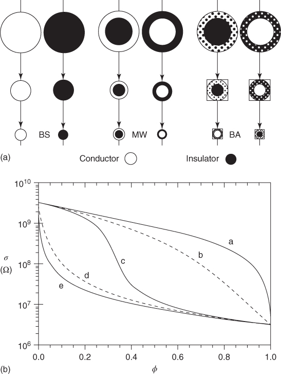
Figure 12.16 Generalized EMT models. (a) Building blocks for the microstructure of the symmetric Bruggeman (BS), Maxwell–Wagner (MW), and asymmetric Bruggeman model (BA). (b) DC conductivity behavior of a matrix (σf = 3.3 × 10⁹ Ω m) as a function of filler volume fraction φ (σf = 3.3 × 10⁶ Ω m) showing the Hashin–Shtrikman bounds or Maxwell–Wagner results (curves a and e), the asymmetric Bruggeman result (curves b and d), and the symmetric Bruggeman result (curve c).
Frequently used is also the Maxwell Garnett model where the conductivity is governed by the equations [61, 64]
which can be solved explicitly to yield [68]
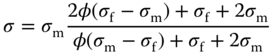
The microstructure can be visualized as built up out of a space‐filling array of coated spheres (Figure 12.16a). The Maxwell Garnett equations are equivalent to the upper and lower bounds as derived by Hashin and Shtrikman [69] for the conductivity of an isotropic two‐component mixture. Since it is assumed that the domains are spatially separated, the model is expected to be valid at low volume fractions.
As an example, we mention an EMT, taking into account the resistivity of the particles and the contact resistivity, that was used to describe the sharp increase in electrical conductivity σ at percolation for antimony‐doped tin oxide (ATO)–acrylate nanocomposite hybrid coatings [70]. The relation between σ and the volume filler fraction φ was analyzed for ATO–acrylate coatings containing ATO nanoparticles grafted with different amounts of 3‐methacryloxypropyltrimethoxysilane coupling agent. Percolation thresholds were observed at low filler fractions (1–2 vol%) for the coatings containing ATO nanoparticles with a low amount of surface grafting. A modified effective medium approximation (EMA) model was introduced for which we refer to the original papers for details. This model takes into consideration different distances between adjacent semiconductive particles in the particle network. The model elucidates how self‐arrangement of the particles influences the location of the percolation threshold in the log σ–φ plot. This modified EMA model could successfully explain the multiple transition behavior and the variable percolation thresholds found for these ATO–acrylate nanocomposite hybrid coatings (Figure 12.17).

Figure 12.17 The experimentally determined σ‐values for various volume fractions of ATO particles and different MPS/ATO ratios (dots), fitted to the modified EMT model (curves).
12.5.3 The Influence of Aspect Ratio
So far we have discussed the effect of isometric particles, that is, particle with a similar dimension in all directions. However, ratio of the largest dimension over the smallest dimension – the aspect ratio − plays an enormous role in both the percolation threshold φcri and the saturation value of the conductivity σsat. Experimental studies have shown that increasing the aspect ratio typically decreases φcri as well as σsat. This behavior can also be modeled, albeit mainly with numerical simulations. As example, Figure 12.18 shows the change in φcri with decreasing aspect ratio [71]. Three simulation models were developed for predicting the electrical conductivity σ and the electrical percolation threshold of polymer composites. The three models are based on finite element modeling (FEM), percolation threshold modeling (PTM), and electrical networks modeling (ENM). A Monte Carlo algorithm was used to construct the geometries, with either soft‐core (overlapping) or hard‐core/soft‐shell (nonoverlapping) fibers. Conductivity measurements on carbon–fiber/PMMA composites with well‐defined fiber aspect ratios were used for experimental validation. The average fiber orientations were calculated from scanning electron micrographs. The soft‐core PTM model with experimental fiber orientations and without adjustable parameters gave accurate (R2 = 0.984) predictions of the electrical percolation threshold as a function of aspect ratio. The corresponding soft‐core ENM model, with close‐contact conductivity calculated with FEM, resulted in good conductivity predictions for the longest fibers, still without the use of any adjustable parameters. The hard‐core/soft‐shell versions of the models, using the shell thickness as an adjustable parameter, gave similar but slightly poorer results.
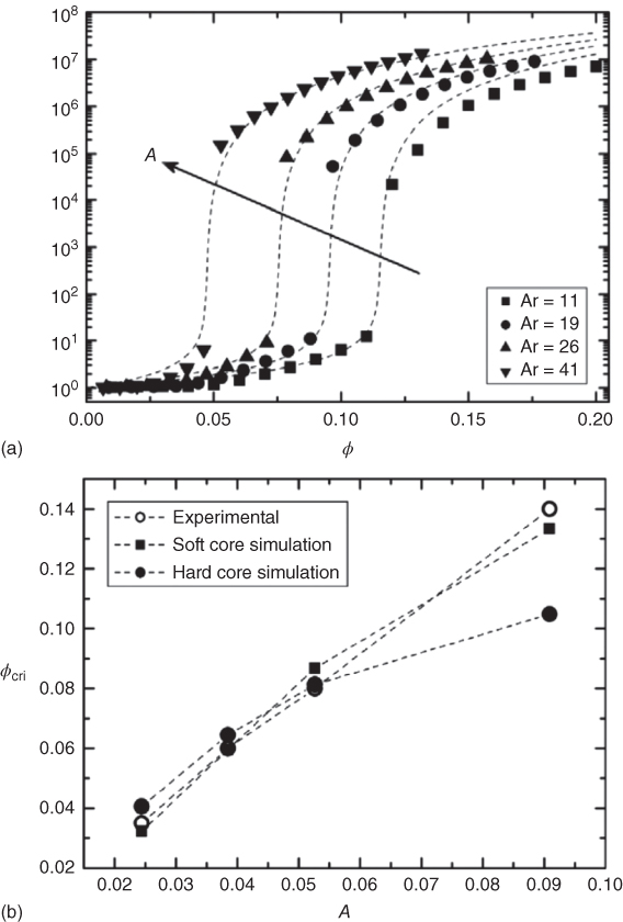
Figure 12.18 Percolation behavior for carbon–fiber/PMMA composites with well‐defined fiber aspect ratios. (a) Normalized conductivity σ/σm as a function of volume fraction φ. The dotted line represent the fit to Eq. 12.40. (b) Experimental and Monte Carlo simulation results for φcri as a function of inverse aspect ratio A with either soft‐core (overlapping) or hard‐core/soft‐shell (nonoverlapping) fibers.
12.5.4 Conductive Particles
As conductive materials for particles, metals and (conductive) oxides are frequently employed. Moreover, carbon materials are used.
While most metals have a decent conductivity, the most conductive ones are the metals Au, Ag, Cu, and Al. The first two are obviously usually too expensive, while the last two suffer from oxidation. In particular, for Al the oxide scale formed is nonconductive, leading easily to high contact resistance, unless plastic deformation occurs during composite formation.
Conductive oxides typically used are tin oxide, indium‐doped tin oxide (ITO), and ATO. Doping is done in order to increase the conductivity. Also in this case the surface of a particle may differ from its bulk [72, 73].
In the category of carbon materials, one distinguishes CB and the more modern variants, buckyballs, CNTs, and graphene. These allotropes can be considered as being formed from sheets of a single layer of atoms, as shown Figure 12.19 [74]. CB belongs to this class of carbonaceous materials, exists in many varieties [75, 76], is a well‐studied and by far the most used nanofiller, and is widely applied for electronic and reinforcement purposes [77]. Recent discoveries in the field of graphitic nanoparticles, in particular CNTs and graphene [78], have allowed the development of materials with exceptional electrical and mechanical properties. Graphite, the most abundant and stable form of carbon, exhibits properties that can be substantially enhanced by exfoliation of its layered structure into single or multilayer sheets [3, 4]. The abovementioned nanoscale powders are commonly incorporated into polymeric matrices to provide enhanced electrical, mechanical, and thermal properties [79–81].
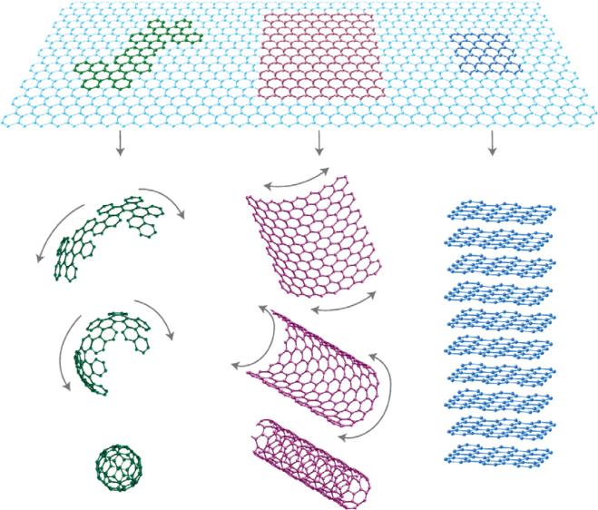
Figure 12.19 The relation between a graphene sheet and buckyballs, carbon nanotubes, and graphite.
Graphene can be considered as a single sheet of graphite, although in practice typically few‐layer graphene is used. The conductivity is in principle as high as for high purity graphite but depends strongly on the amount defects present in the sheet. These defects are introduced during exfoliation, that is, the separation of graphite in single and/or few‐layer sheets, often employing partial oxidation. Removal of defects on exfoliated sheets by reduction appears to be rather difficult, if not impossible. The trick, therefore, is to introduce as limited as possible or no (oxidation and other) defects during exfoliation. Nevertheless, graphene is often functionalized before further use; for example, see [74].
Folding a single sheet to a sphere, one obtains the so‐called buckyballs, also called fullerenes. In C60, hexagons and pentagons of carbon link together in a coordinated fashion to form a hollow, geodesic dome with bonding strains equidistributed among 60 carbon atoms. Other variants include C70, C84, and fullerenes as small as C28 and as large as a postulated C240. Buckyballs were one of the first carbon nanoparticles discovered in 1985 by Smalley, Kroto, and Curl.
CNTs can be considered to be sheets of graphite folded back to become a cylinder. There are various ways to connect two edges of a sheet, and this leads to various types of tubes. In many fabrication processes the resulting CNTs are multiwalled, that is, consist of several concentric cylinders. Single‐walled CNTs are available but are considerably more difficult to fabricate and therefore much more expensive. Various pretreatments are reviewed in [82], properties and applications in [83], and conductivity mechanisms in [84].
A bit of a strange duck in the pond of conducting particles are the phthalocyanines. Although one could expect that materials based on these compounds are highly poisonous and, in fact, the synthesis of these compounds is not without safety pitfalls, the final materials appear to be rather friendly. Figure 12.20 shows as an example the molecular and crystal structure of cyanophthalocyaninato Co(III) (Phthalcon), which contains both NH3 and H2O as ligands. Its behavior in epoxy matrices can be well controlled [85], and the material is used in antistatic coatings [86].
Figure 12.20 The molecular and crystal structure of Phthalcon 11/12.
Obviously, dispersing a sufficient number of conductive particles in a polymer film leads to overall conductivity. Dispersing is done by simple mixing (for rather compatible materials), by high shear mixing (for agglomerated fillers), or on laboratory scale, by sonication. However, dispersing particles will also deteriorate many other properties and, in particular, leads to increased brittleness. The trick is therefore to form strings of conductive particles, so that at low concentration still conductivity emerges. To that purpose, often surfactants are used, in particular for highly incompatible components, such as (somewhat) polar polymers and hydrophobic compounds, like the carbon allotropes [87]. A proper colloidal stability is obviously required to obtain the results desired.
12.6 Some Examples of Conductive Composite Coatings
As is the case for intrinsically conductive polymeric coatings, the literature for composite conductive coatings is large, and we again provide only a few examples. First, we briefly elaborate on the conductivity behavior of polymer composite coatings, in particular for CB–polymer composites, and thereafter address some general issues.
For particulate composites, the conductivity is often described by variable‐range hopping (see Section 12.3.4). Mott [28] showed that this mechanism leads to
where α = 1/(d + 1) and T0 = λa3/kρ(EF) with ρ(EF) the electronic density of states at EF and λ = 16 a dimensionless parameter [88], while for σ0 various expressions were proposed [89, 90]. Experimentally, for the exponent often ![]() or
or ![]() is observed.
is observed.
For some time the variability of the exponent α was assumed to be related to the assumption of constant ρ(EF) (see Section 12.3.4). Writing ρ(E) = ρ0 + cEβ, the expression α = (β + 1)/(β + 2) was derived, which may correspond to a broad particle size distribution [91]. Similarly, writing ρ = c|E|β with β > 0, the expression α = (β + 1)/(β + 4) can be obtained. Although such density of states expressions can explain the observed variability of α, the origin for such expressions remains unclear.
Another explanation is based on the fact that explicit Coulomb interaction between the localized electrons was neglected so far and if included creates a soft or Coulomb gap with width δ around EF [92]. In this case ρ is not constant and leads to ρ(δ) ∼ δ for 2D and ρ(δ) ∼ δ2 for 3D. A crossover takes place between T−1/4 behavior at relatively high temperature (where the Coulomb gap is not active) and T−1/2 behavior at lower temperature. The crossover temperature Tco decreases with donor concentration. A scaling theory was proposed for this crossover reading
where Z = 1/σ is the impedance, A the scaling factor, and h(x) the scaling function h(x) ∼ x−1/4 for x ≫ 1 and h(x) ∼ x−1/2 for x ≪ 1. In fact, the explicit expression
was proposed. This implies that data for various concentrations and temperatures should superimpose. There is some strong experimental evidence from n‐type CdSe crystals [93] to support this explanation.
Although the T−1/2 behavior can be explained by a nonconstant density of states and Coulomb interactions, in other cases these effects are supposed not to play an important role, and a different explanation is called for. For particulate composites, such as CB–polymer composites, fractal behavior of the material is invoked [94]. For these systems there are indications for so‐called superlocalization, in which the wave function ψ decays more than exponentially, that is,
with γ > 1 and L the localization length. Proper analysis leads for the conductivity exponent leads to α = γ /(D + γ) with D the fractal dimension. For incipient percolation clusters, the so‐called Alexander–Orbach conjectureD/γ = 4/3 was used, so that α = 3/7 ≅ 0.43 for both 2D and 3D, close to α = ![]() .
.
However, it was also argued that this cannot be the complete explanation [95], as a distinction has to be made between a typical configuration and the average configuration and that the typical configuration is determining. This leads for 2D to γ ≅ 1.13 ± 0.06 and for 3D to γ ≅ 1.39 ± 0.07. With α = γ /(D + γ), we obtain 0.31 and 0.35 for 2D and 3D, respectively, which leads to the conclusion that the existence of a fractal structure by itself cannot explain the observed T−1/2 behavior of hopping conductivity of semiconductors in which Coulomb interactions are unimportant.
Evidence has been put forward that the effects of both fractality of the particle network (with fractal dimension D) and a variable density of states (described by ρ(E) ∼ Eβ) are important [96]. This led to
With β = 0, D = 3, and γ = 1, we regain the Mott exponent α = ![]() . With β = 0 and D/γ = 4/3 and γ = 1, we regain α = 3/7. The experiments to support this model are well described by σ ∼ (p − pcri)μ with μ = 2.0 ± 0.2, nicely corresponding to the theoretical value. The scaled experimental data as a function of T provided a slope α ≅ 2/3 (Figure 12.21). For a 2D solid, the density of states is given by ρ(E) = c|E| and as CB contains only a few graphene layers, β ≅ 1. With α ≅ 2/3, D/γ ≅ 1.0, suggesting superlocalization. In summary, these results suggest that the combination of a linear density of states and a percolating fractal structure may be responsible for the observed T−1/2 behavior of hopping conductivity of semiconductors when Coulomb interactions are unimportant.
. With β = 0 and D/γ = 4/3 and γ = 1, we regain α = 3/7. The experiments to support this model are well described by σ ∼ (p − pcri)μ with μ = 2.0 ± 0.2, nicely corresponding to the theoretical value. The scaled experimental data as a function of T provided a slope α ≅ 2/3 (Figure 12.21). For a 2D solid, the density of states is given by ρ(E) = c|E| and as CB contains only a few graphene layers, β ≅ 1. With α ≅ 2/3, D/γ ≅ 1.0, suggesting superlocalization. In summary, these results suggest that the combination of a linear density of states and a percolating fractal structure may be responsible for the observed T−1/2 behavior of hopping conductivity of semiconductors when Coulomb interactions are unimportant.
Figure 12.21 Temperature dependence of the conductivity of CB–polymer composites, plotted in the form of ln[σcri/σ(T)] versus T−α for different values of α. (a) α = 1.0, (b) α = 0.70, (c) α = 0.65, (d) α = 0.60, and (e) α = 0.50, showing that the best fit by a straight line is given by α = 0.65 (c).
In the abovementioned experiments, the CB particles were nicely distributed in the matrix so that (simple) percolation theory applies. As indicated before, one would like to manipulate the structure to strings. As a typical example of practical carbon filler‐based polymers, we discuss briefly the work on latex‐based composite coatings employing several carbon allotropes as filler [97].
For manufacturing of composites, latex technology has already been applied, for example, for the incorporation of CNTs into a polymer matrix [18–22] or graphene in polystyrene [12, 23]. The latex approach facilitates the incorporation of nanofillers, via liquid phase mixing, into any kind of highly viscous polymer that can be synthesized by emulsion polymerization or similar processes. This yields highly dispersed filler composites that often have a low (≅1 wt% of filler content) electrical percolation threshold [87].
The carbon nanofillers studied [97] were MWCNTs, graphene, and CB, while graphite was used as reference filler for comparison. The latex was an anionic aqueous emulsion of maleic anhydride modified polypropylene (PP) homopolymer Priex®801, containing 31–33 wt% of solids. All dispersion experiments were carried out with distilled water using sodium dodecylbenzenesulfonate (SDBS) as surfactant. Figure 12.22a shows the evolution of the 268 nm peak in UV–vis characteristic for the exfoliation over sonication time. While a significant difference in the degree of exfoliation was present for graphite on the one hand and the other allotropes at the other hand, a common sonication time of 50 min was chosen for the CNTs and CB and a common sonication time of 120 min for graphene and graphite. From the figure it is clear that for graphite a similar absorbance as for the other allotropes was not reached. For details on the processing, we refer to the original paper [97].
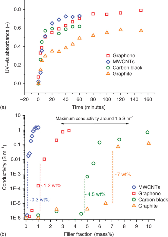
Figure 12.22 Latex‐based carbon composite coatings. (a) UV–vis monitoring of the exfoliation process in water over time following the height of the peak located at about 268 nm for aqueous 0.1 wt% filler solutions (diluted 150 times). (b) Electrical conductivity versus filler mass concentration. To obtain conductivity as function of volume concentration, values must be multiplied by ≅2, which corresponds to the average density of the carbon fillers in g cm−3. Values represent an average of three measurements with standard deviations below 10%.
Figure 12.22b shows that the various allotropes different percolation thresholds were obtained but also that the maximum conductivities are the same within one order of magnitude. Nevertheless, the thresholds obtained are considerably lower than for other processing technologies [98].
It will be clear that proper processing is the key to good properties. While it is generally believed that the conductivity of composites can be quite high, given proper processing, there are clear indications that the final conductivity of particulate polymer composites is limited to the conductivity of a well‐packed network for which the direct contacts provide the leading pathway for charge carriers [99]. Using polymer‐infiltrated single‐walled CNT networks, it was shown that the conductivity only decreased marginally as compared with the noninfiltrated network. Some modeling indicated that the conduction pathways consist mainly of CNTS linked by direct contacts. This renders the prospects for conventional (mixing) processing, with or without surfactants, rather limited. The best option is therefore to realize as much as possible direct contacts by making a particulate network and either infiltrate with polymer or apply further processing, such as photonic sintering and/or rolling [8], to improve the contacts.
References
- 1 Liu, J., Liu, R., Yuan, Y. et al. (2013). Prog. Org. Coat.76: 1251.
- 2 Sander, J. (2010). Anticorrosive Coatings. Köln: Vincentz.
- 3 Ates, M. (2015). J. Adhes. Sci. Technol.30: 1510.
- 4 Qian, Y., Li, Y., Jungwirth, S. et al. (2015). Int. J. Electrochem. Sci.10: 10756.
- 5 Sørensen, P.A., Kiil, S., Dam‐Johansen, K. and Weinell, C.E. (2009). J. Coat. Technol. Res.6: 135.
- 6 Arapov, K.A., Jaakkola, K., Ermolov, V. et al. (2016). Phys. Status Solidi RRL10: 812.
- 7 Lamminen, A., Arapov, K., de With, G. et al. (2017). IEEE Antennas Wirel. Propag. Lett.99: 1.
- 8 Arapov, K., Bex, G., Hendriks, R. et al. (2016). Adv. Eng. Mater.18: 1234.
- 9 van der Pauw, L.J. (1961). Philips Res. Rep.16: 187.
- 10 Foyet, A., Wu, T.H., Kodentsov, A. et al. (2013). J. Electrochem. Soc.160: C159.
- 11 Blythe and Bloor (2005). Chapter 5: Measurement of electrical properties.
- 12 Barsoukov, E. and Ross Macdonald, J. (2005). Impedance Spectroscopy: Theory, Experiment, and Applications, 2e. Hoboken, NJ: Wiley.
- 13 Ghosh, S., Maiyalagan, T. and Basu, R.N. (2016). Nanoscale8: 6921.
- 14 Mott and Davis (1971); Mott (1987).
- 15 Blythe and Bloor (2005).
- 16 Mott, N.F. and Gurney, R.W. (1948). Electronic Processes in Ionic Solids, 2e. Oxford: Oxford University Press.
- 17 Mott (1987).
- 18 Sutton, A.D. (1993). Electronic Structure of Materials. Oxford: Oxford University Press.
- 19 (a) Su, W.P., Schrieffer, J.R. and Heeger, A.J. (1979). Phys. Rev. Lett.42: 1698.(b) Su, W.P., Schrieffer, J.R. and Heeger, A.J. (1980). Phys. Rev.B22: 2099.
- 20 Grant, P.M. and Batra, I.P. (1979). Solid State Commun.29: 225.
- 21 Peierls, R. (1955). Quantum Theory of Solids. Oxford: Oxford University Press.
- 22 Scott, A.C., Chu, F.Y.F. and McLaughlin, D.W. (1973). Proc. IEEE61: 1443.
- 23 Roth, S. (1985). Electronic Properties of Polymers and Related Compounds (ed. H. Kuzmany, M. Mehring and S. Roth), 2. Springer Verlag.
- 24 Ashkenazi, J., Picket, W.E., Klein, B.M. et al. (1987). Synth. Met.21: 503.
- 25 Salem, L. (1966). The Molecular Orbital Theory of Conjugated Systems. New York: Benjamin.
- 26 Anderson, P.W. (1958). Phys. Rev.109: 1492.
- 27 Zojer, E., Knupfer, M., Shuai, Z. et al. (2000). J. Phys. Condens. Matter12: 1753.
- 28 Mott, N.F. (1969). Philos. Mag. 19: 835; see also Mott and Davis (1971).
- 29 Wirix, M.J.M., Bomans, P.H.H., Friedrich, H. et al. (2014). Nano Lett.14: 2033.
- 30 Dang, M.T., Hirsch, L. and Wantz, G. (2011). Adv. Mater.23: 3597.
- 31 Rodd, C.M. and Agarwal, R. (2013). Nano Lett.13: 3760.
- 32 Chou, K.W., Yan, B., Li, R. et al. (2013). Adv. Mater.25: 1923.
- 33 van Bavel, S.S., Sourty, E., de With, G. and Loos, J. (2009). Nano Lett.9: 507.
- 34 Green, M.A., Emery, K., Hishikawa, Y. et al. (2013). Prog. Photovoltaics21: 827.
- 35 Zhang, S., Ye, L., and Hou, J. (2016). Adv. Energy Mater.6: 1502529.
- 36 Krebs, F.C., Espinosa, N., Hösel, M. et al. (2013). Adv. Mater.26: 29.
- 37 (a) Luo, G., Ren, X., Zhang, S. et al. (2016). Small 12: 1547.(b) Joshi, D., Shivanna, R., and Narayan, K.S. (2014). J. Mod. Optics 61: 1703.(c) Mazzio, K.A. and Luscombe, C.K. (2015). Chem. Soc. Rev. 44: 78.
- 38 Brabec, C.J., Scherf, U. and Dyakonov, V. (2014). Organic Photovoltaics, 2e. New York: Wiley.
- 39 Tashiro, K., Minagawa, Y., Kobayashi, M. et al. (1993). Synth. Met.55: 321.
- 40 Winokur, M.J., Spiegel, D., Kim, Y. et al. (1989). Synth. Met.28: C419.
- 41 Dudenko, D., Kiersnowski, A., Shu, J. et al. (2012). Angew. Chem. Int. Ed.51: 11068.
- 42 Wirix, M.J.M., Bomans, P.H.H., Hendrix, M.M.R.M. et al. (2015). J. Mater. Chem.A3: 5031.
- 43 Yu, G., Gao, J., Hummelen, J.C. et al. (1995). Science270: 1789.
- 44 Yang, X.N., Loos, J., Veenstra, S.C. et al. (2005). Nano Lett.5: 579.
- 45 Chen, D. and Zachmann, H.G. (1991). Polymer32: 1612.
- 46 Huesmann, D., DiCarmine, P.M. and Seferos, D.S. (2011). J. Mater. Chem.21: 408.
- 47 Brinkmann, M. (2011). J. Polym. Sci., Part B: Polym. Phys. 49: 1218.
- 48 Sun, S., Salim, T., Wong, L.H. et al. (2011). J. Mater. Chem.21: 377.
- 49 Berson, S., De Bettignies, R., Bailly, S. and Guillerez, S. (2007). Adv. Funct. Mater.17: 1377.
- 50 Azimi, H., Fournier, D., Wirix, M. et al. (2012). Org. Electron.13: 1315.
- 51 Fisher, M.E. (1971). Critical Phenomena: Enrico Fermi Summer School (ed. M.S. Green). New York: Academic Press.
- 52 Levinshtein, M., Shur, M.S. and Efros, E.L. (1976). Sov. Phys.‐JETP42: 1120.
- 53 Sahimi, M. and Arbabi, A. (1991). J. Stat. Phys.62: 453.
- 54 Clerc, J.P., Giraud, G., Alexander, S. and Guyos, E. (1980). Phys. Rev.B22: 2489.
- 55 Scher, H. and Zallen, R. (1971). J. Chem. Phys.53: 3759.
- 56 Harris, A.B. (1974). J. Phys.C7: 1671.
- 57 Sahimi, M. (1994). Applications of Percolation Theory. London: Taylor and Francis.
- 58 Strümpler, R. and Glatz‐Reichenbach, J. (1999). J. Electroceram.3: 329.
- 59 Stauffer, D. and Aharoni, A. (1994). Introduction to Percolation Theory, 2e. London: Taylor and Francis.
- 60 Lux, F. (1993). J. Mater. Sci.26: 285.
- 61 Landauer, R. (1978). Electrical transport and Optical Properties of Inhomogeneous Media. In: AIP Conference of Proceedings (ed. J.C. Garland and D.B. Tanner), 2. New York.
- 62 McLachlan, D.S., Blaszkiewics, M. and Newnham, R.E. (1990). J. Am. Ceram. Soc.73: 2187.
- 63 McLachlan, D.S. (2000). J. Electroceram.5: 93.
- 64 Choy, T. (1999). Effective Medium Theory. Oxford: Oxford University Press.
- 65 Kirkpatrick, S. (1973). Rev. Mod. Phys.45: 574.
- 66 Zallen (1983).
- 67 McLachlan, D.S., Huang, J.H. and Mason, T.O. (2000). J. Electroceram.5: 37.
- 68 Levy, O. and Stroud, D. (1997). Phys. Rev.B56: 8035.
- 69 Bergman, D.J. and Stroud, D. (1992). Solid State Physics, vol. 46, 147. San Diego: Academic Press.
- 70 Soloukhin, V.A., Brokken‐Zijp, J.C.M. and de With, G. (2007). J. Polym. Sci., Part B: Polym. Phys. 45: 2147.
- 71 Nilsson, F., Krückel, J., Schubert, D.W. et al. (2016). Compos. Sci. Technol.132: 16.
- 72 Brokken‐Zijp, J.C.M., van Asselen, O.L.J., Kleinjan, W.E. et al. (2010). J. Nanotechnnol., Article ID 579708.
- 73 Kleinjan, W.E., Brokken‐Zijp, J.C.M., van de Belt, R. et al. (2008). J. Mater. Res.23: 869.
- 74 Kuila, T., Bose, S., Mishra, A.K. et al. (2012). Prog. Mater Sci.57: 1061.
- 75 Huang, J.‐C. (2002). Adv. Polym. Tech.21: 299.
- 76 Brigandi, P.J., Cogen, J.M. and Pearson, R.A. (2014). Polym. Eng. Sci.54: 1.
- 77 Donnet, J.B. (2003). Compos. Sci. Technol.63: 1085.
- 78 Novoselov, K.S., Geim, A.K., Morozov, S.V. et al. (2004). Science306: 666.
- 79 Moniruzzaman, M. and Winey, K. (2006). Macromolecules39: 5194.
- 80 Stankovich, S., Dikin, D.A., Dommett, G.H.B. et al. (2006). Nature442: 282.
- 81 Ghislandi, M., Tkalya, E., Schillinger, S. et al. (2013). Compos. Sci. Technol.80: 16.
- 82 Bose, S., Khare, R.A. and Moldenaers, P. (2010). Polymer51: 975.
- 83 Ibrahim, S.K. (2013). Carbon Lett.14: 131.
- 84 Min, C., Shen, X., Shi, Z. et al. (2010). Polym. Plast. Technol. Eng.49: 1172.
- 85 Yuan, M., Brokken‐Zijp, J.C.M. and de With, G. (2009). J. Polym. Sci., Part B: Polym. Phys. 47: 366.
- 86 Yuan, M., Brokken‐Zijp, J.C.M. and de With, G. (2010). Eur. Polym. J.46: 86.
- 87 Tkalya, E.E., Ghislandi, M., de With, G. and Koning, C.E. (2012). Curr. Opin. Colloid Interface Sci.17: 225.
- 88 Ambegaokar, V., Halperin, B.I. and Langer, J.S. (1971). Phys. Rev. B4: 2612.
- 89 (a) Movaghar, B., Pohlmann, B. and Schirmacher, W. (1980). Philos. Mag. B41: 49.(b) Movaghar, B., Pohlmann, B. and Schirmacher, W. (1980). Solid State Commun. 34: 451.(c) Movaghar, B. and Schirmacher, W. (1981). J. Phys. C14: 859.
- 90 (a) Butcher, P.N. and McInnes, J.A. (1979). Philos. Mag. 32: 249.(b) Butcher, P.N. (1980). Philos. Mag. B42: 799.
- 91 Mehbod, M., Wyder, P., Deltour, R. et al. (1987). Phys. Rev. B36: 7627.
- 92 Efros, A.L. and Shklovskii, B.I. (1975). J. Phys. C8: L49.
- 93 Zhang, Y., Dai, P., Levy, M. and Sarachik, M.P. (1990). Phys. Rev. Lett.64: 2687.
- 94 Deutscher, G., Levy, Y. and Souillard, B. (1987). Europhys. Lett.4: 577.
- 95 (a) Harris, A.B. and Aharony, A. (1987). Europhys. Lett. 4: 1355.(b) Aharony, A. and Harris, A.B. (1990). PhysicaA163: 38.
- 96 (a) van der Putten, D., Moonen, J.T., Brom, H.B. et al. (1992). Phys. Rev. Lett. 69: 494.(b) Aharany, A. and Harris, A.B. (1993). Phys. Rev. Lett. 70: 4160.(c) Michels, M.A.J., Brokken‐Zijp, J.C.M., van der Putten, D. et al. (1993). Phys. Rev. Lett.70: 4161.
- 97 Ghislandi, M., Tkalya, E., Marinho, B. et al. (2013). Composites Part AA53: 145.
- 98 Grossiord, N., Loos, J. and Koning, C.E. (2005). J. Mater. Chem.15: 2349.
- 99 Bârsan, O.A., Hoffmann, G.G., van der Ven, L.G.J. and de With, G. (2016). Adv. Funct. Mater.26: 4377.
Further Reading
- Barford, W. (2005). Electronic and Optical Properties of Conjugated Polymers. Oxford: Oxford University Press.
- Blythe, T. and Bloor, D. (2005). Electrical Properties of Polymers, 2e. Cambridge: Cambridge University Press.
- Chien, J.C.W. (1984). Polyacetylene: Chemistry, Physics, and Material Science. Orlando: Academic Press.
- Farges, J.‐P. (1994). Organic Conductors. New York: Marcel Dekker.
- Mott, N.F. and Davis, E.A. (1971). Electronic Processes in Non‐crystalline Materials, 2e. Oxford: Clarendon Press.
- Mott, N.F. (1987). Conduction in Non‐crystalline Solids. Oxford: Oxford University Press.
- Skotheim, T.A. and Reynolds, J.R. (2007). Handbook of Conducting Polymers, 3e. New York: Marcel Dekker.
- Wan, M. (2008). Conducting Polymers with Micro or Nanometer Structure. Beijing: Springer Science and Business Media.
- Zallen, R. (1983). The Physics of Amorphous Solids. New York: Wiley.