
12
SYNTHESIS OF DC AND LOW-FREQUENCY SINUSOIDAL AC VOLTAGES FOR MOTOR DRIVES, UPS, AND POWER SYSTEMS APPLICATIONS
12.1 INTRODUCTION
The importance of power electronics applications for motor drives (AC and DC), UPS, and in power systems was described in Chapter 11. In many of these applications, the voltage-link structure of Figure 12.1 is used, where our emphasis will be to discuss how the load-side converter, with the DC voltage as input, synthesizes DC or low-frequency sinusoidal voltage outputs. Functionally, this converter operates as a linear amplifier, amplifying a control signal, DC in case of DC motor drives, and AC in case of AC motor drives, UPS, and other utility-related applications. The power flow through this converter should be reversible.

FIGURE 12.1 Voltage-link system.
These converters consist of bidirectional switching power-poles, discussed in Chapter 3, two in the case of DC motor drives and single-phase AC applications, and three in the case of AC motor drives and three-phase applications. These are shown for DC and AC motor drives in Figures 12.2a and 12.2b, respectively.

FIGURE 12.2 Converters for DC and AC motor drives.
12.2 BIDIRECTIONAL SWITCHING POWER-POLE AS THE BUILDING BLOCK
In buck and boost DC-DC converters, discussed in Chapter 3, implementation of the switching power-pole by one transistor and one diode dictates the instantaneous current flow to be unidirectional. However, as shown in Figure 12.3a, combining the switching power-pole implementations of buck and boost converters, where the two transistors are switched by complementary signals, allows a continuous bidirectional power and current capability. In such a bidirectional switching power-pole, the positive inductor current ![]() as shown in Figure 12.3b, represents a buck-mode of operation, where only the transistor and the diode associated with the buck converter take part. The transistor conducts during
as shown in Figure 12.3b, represents a buck-mode of operation, where only the transistor and the diode associated with the buck converter take part. The transistor conducts during ![]() , and the diode conducts during
, and the diode conducts during ![]() . Similarly, as shown in Figure 12.3c, the negative inductor current represents a boost-mode of operation, where only the transistor and the diode associated with the boost converter take part. The transistor conducts during
. Similarly, as shown in Figure 12.3c, the negative inductor current represents a boost-mode of operation, where only the transistor and the diode associated with the boost converter take part. The transistor conducts during ![]() (
(![]() ), and the diode conducts during
), and the diode conducts during ![]() (
(![]() ).
).

FIGURE 12.3 Bidirectional power flow through a switching power-pole.
Figures 12.3b and 12.3c show that the combination of devices in Figure 12.3a renders it to be a switching power-pole that can carry ![]() in either direction. This is shown as an equivalent switch in Figure 12.4a that is effectively in the “up” position when
in either direction. This is shown as an equivalent switch in Figure 12.4a that is effectively in the “up” position when ![]() , as shown in Figure 12.4b, and in the “down” position when
, as shown in Figure 12.4b, and in the “down” position when ![]() , as shown in Figure 12.4c, regardless of the direction of
, as shown in Figure 12.4c, regardless of the direction of ![]() .
.

FIGURE 12.4 Bidirectional switching power-pole.
The bidirectional switching power-pole of Figure 12.4a is repeated in Figure 12.5a for pole-a, with its switching signal identified as ![]() . In response to the switching signal, it behaves similarly to the switching power-pole in Chapter 3: “up” when
. In response to the switching signal, it behaves similarly to the switching power-pole in Chapter 3: “up” when ![]() and otherwise “down.” Therefore, its switching-cycle-averaged representation is also an ideal transformer, shown in Figure 12.5b, with a turns ratio
and otherwise “down.” Therefore, its switching-cycle-averaged representation is also an ideal transformer, shown in Figure 12.5b, with a turns ratio ![]() .
.

FIGURE 12.5 Switching-cycle-averaged representation of the bidirectional power pole.
The switching-cycle-averaged values of the variables at the voltage port and the current port in Figure 12.5b are related by ![]() as follows:
as follows:
We should note that, ideally, unlike switching power-poles with a single transistor, discussed in Chapter 3, no discontinuous-conduction mode exists in a bidirectional switching pole of Figure 12.5a.
12.2.1 Pulse-Width Modulation (PWM) of the Bidirectional Switching Power-Pole
The voltage of a switching power-pole at the current port is always of positive polarity. However, the output voltages of converters in Figure 12.2 for motor drives and other AC applications must be reversible in polarity. This is achieved by introducing a common-mode voltage in each power pole as discussed below and taking the differential output between the power poles.
To obtain the desired switching-cycle-averaged voltage ![]() in Figure 12.5, which includes the common-mode voltage, requires the following power-pole duty ratio from Equation 12.1:
in Figure 12.5, which includes the common-mode voltage, requires the following power-pole duty ratio from Equation 12.1:
where ![]() is the DC-bus voltage. To obtain the switching signal
is the DC-bus voltage. To obtain the switching signal ![]() to deliver this duty ratio, a control voltage
to deliver this duty ratio, a control voltage ![]() is compared with a triangular-shaped carrier waveform of the switching frequency
is compared with a triangular-shaped carrier waveform of the switching frequency ![]() and amplitude
and amplitude ![]() , as shown in Figure 12.6. Because of symmetry, only
, as shown in Figure 12.6. Because of symmetry, only ![]() , one-half of the switching time period, needs to be considered. The switching-signal
, one-half of the switching time period, needs to be considered. The switching-signal ![]() if
if ![]() and is otherwise
and is otherwise ![]() . Therefore in Figure 12.6,
. Therefore in Figure 12.6,

FIGURE 12.6 Waveforms for PWM in a switching power-pole.
The switching-cycle-averaged representation of the switching power-pole in Figure 12.7a is shown by a controllable turn-ratio ideal transformer in Figure 12.7b, where the switching-cycle-averaged representation of the duty-ratio control is in accordance with Equation 12.4.

FIGURE 12.7 Switching power-pole and its duty-ratio control.
The reason for selecting a triangular carrier-signal waveform, as opposed to a ramp signal in DC-DC converters of Chapter 3, is that it minimizes the harmonic content in the output voltage waveform for a given frequency with which the converter devices are switched. The Fourier spectrum of the switching waveform ![]() is shown in Figure 12.8, which depends on the nature of the control signal. If the control voltage is DC, the output voltage has harmonics at the multiples of the switching frequency, that is at
is shown in Figure 12.8, which depends on the nature of the control signal. If the control voltage is DC, the output voltage has harmonics at the multiples of the switching frequency, that is at ![]() ,
, ![]() , and so on, as shown in Figure 12.8a. If the control voltage varies at a low frequency
, and so on, as shown in Figure 12.8a. If the control voltage varies at a low frequency ![]() , as in AC motor drives and UPS, then the harmonics of significant magnitudes appear in the side bands of the switching frequency and its multiples, as shown in Figure 12.8b, where
, as in AC motor drives and UPS, then the harmonics of significant magnitudes appear in the side bands of the switching frequency and its multiples, as shown in Figure 12.8b, where

FIGURE 12.8 Harmonics in the output of a switching power-pole.
in which ![]() and
and ![]() are constants that can take on values 1, 2, 3, and so on. Some of these harmonics associated with each power pole are canceled from the converter output voltages, where two or three of such power poles are used.
are constants that can take on values 1, 2, 3, and so on. Some of these harmonics associated with each power pole are canceled from the converter output voltages, where two or three of such power poles are used.
In the power pole shown in Figure 12.7, the output voltage ![]() and its switching-cycle-averaged
and its switching-cycle-averaged ![]() are limited between
are limited between ![]() and
and ![]() . To obtain an output voltage
. To obtain an output voltage ![]() (where “n” may be a fictitious node) that can become both positive and negative, a common-mode offset
(where “n” may be a fictitious node) that can become both positive and negative, a common-mode offset ![]() is introduced in each power pole so that the pole output voltage is
is introduced in each power pole so that the pole output voltage is
where ![]() allows
allows ![]() to become both positive and negative around the common-mode voltage
to become both positive and negative around the common-mode voltage ![]() . In the differential output, when two or three power poles are used, the common-mode voltage gets eliminated.
. In the differential output, when two or three power poles are used, the common-mode voltage gets eliminated.
12.3 CONVERTERS FOR DC MOTOR DRIVES ( )
)
Converters for DC motor drives consist of two power poles, as shown in Figure 12.9a, where

FIGURE 12.9 Converter for DC motor drive.
and ![]() can assume both positive and negative values. Since the output voltage is desired to be in a full range, from
can assume both positive and negative values. Since the output voltage is desired to be in a full range, from ![]() to
to ![]() , pole-a is assigned to produce
, pole-a is assigned to produce ![]() , and pole-b is assigned to produce
, and pole-b is assigned to produce ![]() toward the output:
toward the output:
where “n” is a fictitious node, as shown in Figure 12.9a, chosen to define the contribution of each pole toward ![]() .
.
To achieve equal excursions in positive and negative values of the switching-cycle-averaged output voltage, the switching-cycle-averaged common-mode voltage in each pole is chosen to be one-half the DC-bus voltage,
Therefore, from Equation 12.6,
The switching-cycle-averaged output voltages of the power poles and the converter are shown in Figure 12.9b. From Equations 12.3 and 12.10,
and from Equation 12.11,
Example 12.1
In a DC motor drive, the DC-bus voltage is ![]() . Determine the following:
. Determine the following: ![]() ,
, ![]() , and
, and ![]() for pole-a and similarly for pole-b, if the output voltage required is (a)
for pole-a and similarly for pole-b, if the output voltage required is (a) ![]() and (b)
and (b) ![]() .
.
Solution From Equation 12.9, ![]() .
.
a. For ![]() , from Equation 12.8,
, from Equation 12.8, ![]() and
and ![]() . From Equation 12.10,
. From Equation 12.10, ![]() and
and ![]() . From Equation 12.11,
. From Equation 12.11, ![]() and
and ![]() .
.
b. For ![]() ,
, ![]() and
and ![]() . Therefore from Equation 12.10,
. Therefore from Equation 12.10, ![]() and
and ![]() . From Equation 12.11,
. From Equation 12.11, ![]() and
and ![]() .
.
The switching-cycle-averaged representation of the two power poles, along with the pulse-width modulator, in a block diagram form is shown in Figure 12.10.

FIGURE 12.10 Switching-cycle-averaged representation of the converter for DC drives.
In each power pole of Figure 12.10, the switching-cycle-averaged DC-side current is related to its output current by the pole duty ratio,
By Kirchhoff’s current law, the total switching-cycle-averaged DC-side current is
Recognizing the directions with which the currents ![]() and
and ![]() are defined,
are defined,
Thus, substituting currents from Equation 12.14 into Equation 12.15,
Example 12.2
In the DC motor drive of Example 12.1, the output current into the motor is ![]() . Calculate the power delivered from the DC-bus and show that it is equal to the power delivered to the motor (assuming the converter to be lossless), if
. Calculate the power delivered from the DC-bus and show that it is equal to the power delivered to the motor (assuming the converter to be lossless), if ![]() .
.
Solution Using the values for ![]() and
and ![]() from part (a) of Example 12.1, and
from part (a) of Example 12.1, and ![]() from Equation 12.16,
from Equation 12.16, ![]() and therefore the power delivered by the DC-bus is
and therefore the power delivered by the DC-bus is ![]() . Power delivered by the converter to the motor is
. Power delivered by the converter to the motor is ![]() , which is equal to the input power (neglecting the round-off errors).
, which is equal to the input power (neglecting the round-off errors).
Using Equations 12.4 and 12.11, the control voltages for the two poles are as follows:
In Equation 12.17, defining the second term in the two control voltages above as one-half the control voltage, that is,
Equation 12.18 simplifies as follows:
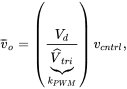 (12.19)
where ![]() is the converter gain
is the converter gain ![]() , from the feedback control signal to the switching-cycle-averaged voltage output, as shown in Figure 12.11 in a block diagram form.
, from the feedback control signal to the switching-cycle-averaged voltage output, as shown in Figure 12.11 in a block diagram form.

FIGURE 12.11 Gain of the converter for DC drives.
12.3.1 Switching Waveforms in a Converter for DC Motor Drives
We will look further into the switching details of the converter in Figure 12.9a. To produce a positive output voltage, the control voltages are shown in Figure 12.12. Only one-half of the time period, ![]() , needs to be considered due to symmetry.
, needs to be considered due to symmetry.

FIGURE 12.12 Switching voltage waveforms in a converter for DC drive.
The pole output voltages ![]() and
and ![]() have the same waveform as the switching signals except for their amplitude. The output voltage
have the same waveform as the switching signals except for their amplitude. The output voltage ![]() waveform shows that the effective switching frequency at the output is twice the original. That is, within the time period of the switching frequency
waveform shows that the effective switching frequency at the output is twice the original. That is, within the time period of the switching frequency ![]() with which the converter devices are switching, there are two complete cycles of repetition. Therefore, the harmonics in the output are at
with which the converter devices are switching, there are two complete cycles of repetition. Therefore, the harmonics in the output are at ![]() and at its multiples. If the switching frequency is selected sufficiently large, the motor inductance may be enough to keep the ripple in the output current within an acceptable range without the need for an external inductor in series.
and at its multiples. If the switching frequency is selected sufficiently large, the motor inductance may be enough to keep the ripple in the output current within an acceptable range without the need for an external inductor in series.
Next, we will look at the currents associated with this converter, repeated in Figure 12.13. The pole currents ![]() and
and ![]() . The DC-side current
. The DC-side current ![]() . The waveforms for these currents are shown by means of Example 12.3.
. The waveforms for these currents are shown by means of Example 12.3.

FIGURE 12.13 Currents defined in the converter for DC motor drives.
Example 12.3
In the DC motor drive of Figure 12.13, assume the operating conditions are as follows: ![]() ,
, ![]() , and
, and ![]() . The switching frequency
. The switching frequency ![]() is 20 kHz. Assume that the series resistance
is 20 kHz. Assume that the series resistance ![]() associated with the motor is
associated with the motor is ![]() . Calculate the series inductance
. Calculate the series inductance ![]() necessary to keep the peak-peak ripple in the output current to be
necessary to keep the peak-peak ripple in the output current to be ![]() at this operating condition. Assume that
at this operating condition. Assume that ![]() . Plot
. Plot ![]() ,
, ![]() ,
, ![]() , and
, and ![]() .
.
Solution As seen from Figure 12.12, the output voltage ![]() is a pulsating waveform that consists of a DC switching-cycle-averaged
is a pulsating waveform that consists of a DC switching-cycle-averaged ![]() plus a ripple component
plus a ripple component ![]() , which contains sub-components that are at very high frequencies (the multiples of
, which contains sub-components that are at very high frequencies (the multiples of ![]() ):
):
Therefore, the resulting current ![]() consists of a switching-cycle-averaged DC component
consists of a switching-cycle-averaged DC component ![]() and a ripple component
and a ripple component ![]() :
:
For a given ![]() , we can calculate the output current by means of superposition by considering the circuit at DC and the ripple frequency (the multiples of
, we can calculate the output current by means of superposition by considering the circuit at DC and the ripple frequency (the multiples of ![]() ), as shown in Figures 12.14a and 12.14b, respectively. In the DC circuit, the series inductance has no effect and hence is omitted from Figure 12.14a. In the ripple-frequency circuit of Figure 12.14b, the back-emf
), as shown in Figures 12.14a and 12.14b, respectively. In the DC circuit, the series inductance has no effect and hence is omitted from Figure 12.14a. In the ripple-frequency circuit of Figure 12.14b, the back-emf ![]() , that is DC, is suppressed along with the series resistance
, that is DC, is suppressed along with the series resistance ![]() , which generally is negligible compared to the inductive reactance of
, which generally is negligible compared to the inductive reactance of ![]() at very frequencies associated with the ripple.
at very frequencies associated with the ripple.

FIGURE 12.14 Superposition of DC and ripple-frequency variables.
From the circuit of Figure 12.14a,
The switching waveforms are shown in Figure 12.15, which is based on Figure 12.12, where the details are shown for the first half-cycle. The output voltage ![]() pulsates between
pulsates between ![]() and
and ![]() , where from Equation 12.11,
, where from Equation 12.11, ![]() , and
, and ![]() . At
. At ![]() ,
, ![]() . Using Equations 12.20 and 12.22, the ripple voltage waveform is also shown in Figure 12.15, where during
. Using Equations 12.20 and 12.22, the ripple voltage waveform is also shown in Figure 12.15, where during ![]() , the ripple voltage in the circuit of Figure 12.14b is
, the ripple voltage in the circuit of Figure 12.14b is ![]() . Therefore, during this time interval, the peak-to-peak ripple
. Therefore, during this time interval, the peak-to-peak ripple ![]() in the inductor current can be related to the ripple voltage as follows:
in the inductor current can be related to the ripple voltage as follows:

FIGURE 12.15 Switching current waveforms in Example 12.3.
Substituting the values in the equation above with ![]() ,
, ![]() . As shown in Figure 12.15, the output current increases linearly during
. As shown in Figure 12.15, the output current increases linearly during ![]() , and its waveform is symmetric around the switching-cycle-averaged value; that is, it crosses the switching-cycle-averaged value at the midpoint of this interval. The ripple waveform in other intervals can be found by symmetry. The DC-side current
, and its waveform is symmetric around the switching-cycle-averaged value; that is, it crosses the switching-cycle-averaged value at the midpoint of this interval. The ripple waveform in other intervals can be found by symmetry. The DC-side current ![]() flows only during
flows only during ![]() interval; otherwise, it is zero, as shown in Figure 12.15. Averaging over
interval; otherwise, it is zero, as shown in Figure 12.15. Averaging over ![]() , the switching-cycle-averaged DC-side current
, the switching-cycle-averaged DC-side current ![]() .
.
12.4 SYNTHESIS OF LOW-FREQUENCY AC
The principle of synthesizing a DC voltage for DC motor drives can be extended for synthesizing low-frequency AC voltages, so long as the frequency ![]() of the AC being synthesized is two or three orders of magnitude smaller than the switching frequency
of the AC being synthesized is two or three orders of magnitude smaller than the switching frequency ![]() . This is the case in most AC motor drives and UPS applications where
. This is the case in most AC motor drives and UPS applications where ![]() is at 60 Hz (or is of the order of 60 Hz) and the switching frequency is a few tens of a kilohertz. The control voltage, which is compared with a triangular waveform voltage to generate switching signals, varies slowly at the frequency
is at 60 Hz (or is of the order of 60 Hz) and the switching frequency is a few tens of a kilohertz. The control voltage, which is compared with a triangular waveform voltage to generate switching signals, varies slowly at the frequency ![]() of the AC voltage being synthesized.
of the AC voltage being synthesized.
Therefore, with ![]() , during a switching-frequency time period
, during a switching-frequency time period ![]() , the control voltage can be considered pseudo-DC, and the analysis and synthesis for the converter for DC drives applies. Figure 12.16 shows how the switching power-pole output voltage can be synthesized so, on switching-cycle-averaged, it varies as shown at the low frequency
, the control voltage can be considered pseudo-DC, and the analysis and synthesis for the converter for DC drives applies. Figure 12.16 shows how the switching power-pole output voltage can be synthesized so, on switching-cycle-averaged, it varies as shown at the low frequency ![]() , where at any instant “under the microscope” shows the switching signal waveform with the duty ratio that depends on the switching-cycle-averaged voltage being synthesized. The limit on switching-cycle-averaged power-pole voltage is between
, where at any instant “under the microscope” shows the switching signal waveform with the duty ratio that depends on the switching-cycle-averaged voltage being synthesized. The limit on switching-cycle-averaged power-pole voltage is between ![]() and
and ![]() , as in the case of converters for DC drives.
, as in the case of converters for DC drives.
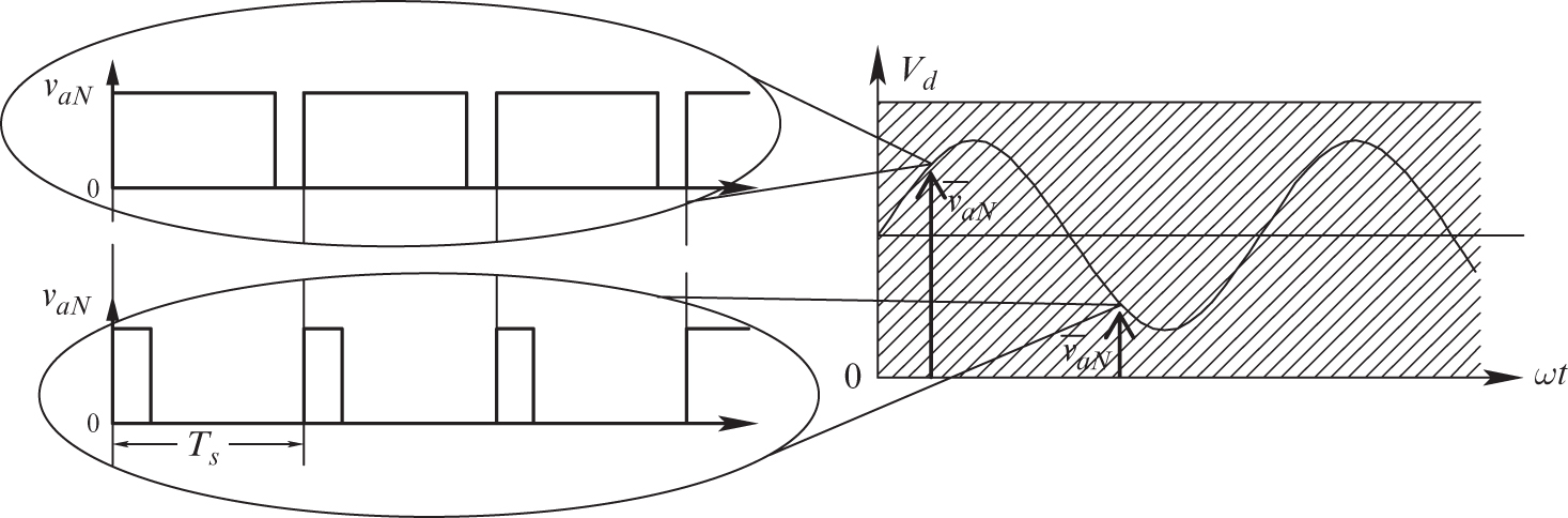
FIGURE 12.16 Waveforms of a switching power-pole to synthesize low-frequency AC.
The switching-cycle-averaged representation of the switching power-pole in Figure 12.5a is, as shown earlier in Figure 12.5b, represented by an ideal transformer with a controllable turns ratio. The harmonics in the output of the power pole in a general form were shown earlier by Figure 12.8b. In the following sections, two switching power-poles are used to synthesize single-phase AC voltage for single-phase UPS and for interfacing with a single-phase supply voltage, and three switching power-poles are used to synthesize three-phase AC for motor drives, UPS, and utility-related applications.
12.5 SINGLE-PHASE INVERTERS
The load-side converter of 1-phase UPS, or for interfacing with the single-phase utility grid, is similar in power topology to that in DC motor drives, as shown in Figure 12.17a. The switching-cycle-averaged representation is shown in Figure 12.17b. It consists of two switching power-poles where, as shown, the inductance of the low-pass filter establishes the current ports of the two power poles.

FIGURE 12.17 Single-phase uninterruptible power supply.
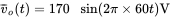
The switching-cycle-averaged voltages being synthesized are shown in Figure 12.18, which in this application are sinusoidal at the line frequency ![]() ,
,

FIGURE 12.18 Switching-cycle-averaged voltages in a single-phase UPS.
Similar to DC motor drives, the common-mode voltage is
and the pole output voltages with respect to a hypothetical neutral “n” are
Therefore, as shown in Figure 12.18, the switching-cycle-averaged voltages are as follows:
On the DC-side, in order to calculate the switching-cycle-averaged current drawn from the DC source, we will assume that the switching-cycle-averaged AC-side current is sinusoidal and lagging behind the output AC voltage ![]() by an angle
by an angle ![]() , as shown in Figure 12.19:
, as shown in Figure 12.19:
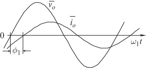
FIGURE 12.19 Output voltage and current.
Assuming the ripple in the output current to be negligible, the average output power equals the product of the switching-cycle-averaged output voltage ![]() and the switching-cycle-averaged output current
and the switching-cycle-averaged output current ![]() ,
,
Assuming the converter to be lossless, the switching-cycle-averaged input current can be calculated by equating the input power to the average power:
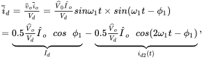 (12.30)
which shows that the switching-cycle-averaged current drawn from the DC-bus has a DC component ![]() that is responsible for the average power transfer to the AC side of the converter, and a second harmonic component
that is responsible for the average power transfer to the AC side of the converter, and a second harmonic component ![]() (at twice the frequency of the AC output), which is undesirable. The DC-link storage in a 1-phase inverter must be sized to accommodate the flow of this large AC current at twice the output frequency, similar to that in PFCs, discussed in Chapter 6. Of course, we should not forget that the above discussion is in terms of switching-cycle-averaged representation of the switching power-poles. Therefore, the DC-link capacitor must also accommodate the flow of switching-frequency ripple in
(at twice the frequency of the AC output), which is undesirable. The DC-link storage in a 1-phase inverter must be sized to accommodate the flow of this large AC current at twice the output frequency, similar to that in PFCs, discussed in Chapter 6. Of course, we should not forget that the above discussion is in terms of switching-cycle-averaged representation of the switching power-poles. Therefore, the DC-link capacitor must also accommodate the flow of switching-frequency ripple in ![]() , discussed below. The pulsating current ripple in
, discussed below. The pulsating current ripple in ![]() can be bypassed from being supplied by the batteries by placing a high-quality capacitor with a very low equivalent series inductance in close physical proximity to the converter switches.
can be bypassed from being supplied by the batteries by placing a high-quality capacitor with a very low equivalent series inductance in close physical proximity to the converter switches.
12.5.1 Switching Waveforms Associated with a Single-Phase Inverter
The switching waveforms in a single-phase converter are shown by means of an example below.
Example 12.4
In a single-phase UPS, shown in Figure 12.17a, the parameters and the operating conditions are as follows: ![]() ,
, ![]() ,
, ![]() volts, and the switching frequency
volts, and the switching frequency ![]() . At the positive peak of the voltage waveform to be synthesized, calculate and plot the switching waveforms for one cycle of the switching frequency.
. At the positive peak of the voltage waveform to be synthesized, calculate and plot the switching waveforms for one cycle of the switching frequency.
At the positive peak, the switching-cycle-averaged voltage to be synthesized is ![]() . Therefore, using the equations for the DC drive converters, from Equation 12.11,
. Therefore, using the equations for the DC drive converters, from Equation 12.11, ![]() and
and ![]() , where
, where ![]() . Assuming
. Assuming ![]() , from Equation 12.4,
, from Equation 12.4, ![]() , and
, and ![]() . The resulting voltage waveforms are shown in Figure 12.20.
. The resulting voltage waveforms are shown in Figure 12.20.

FIGURE 12.20 Waveforms in the UPS of Example 12.4.
As shown in Figure 12.20, the output voltage waveform pulsates at the switching frequency, and a low-pass filter is necessary to remove the output voltage harmonics, which were discussed earlier in a generic manner for each switching power-pole and expressed by Equation 12.5.
12.5.2 Simulation and Hardware Prototyping
The simulation of a single-phase inverter is demonstrated by means of an example:
Example 12.5
A single-phase inverter is connected to an ![]() load,
load, ![]() , and
, and ![]() . The DC voltage
. The DC voltage ![]() . The desired output voltage is
. The desired output voltage is ![]() RMS at
RMS at ![]() . Simulate this converter using LTspice.
. Simulate this converter using LTspice.
Solution
The simulation file used in this example is available on the accompanying website. The LTspice model is shown in Figure 12.21, and the steady-state waveforms from the simulation of this converter are shown in Figure 12.22.

FIGURE 12.21 LTspice model.

FIGURE 12.22 LTspice simulation results.
The same control algorithm used in Example 12.5 is implemented in Workbench, as shown in Figure 12.23, to generate a sinusoidal voltage from DC using the Sciamble lab kit.

FIGURE 12.23 Workbench model.
In the hardware, the available DC-bus voltage is ![]() ,and this is used to generate a
,and this is used to generate a ![]() RMS,
RMS, ![]() output voltage, as shown in Figure 12.24. The switching frequency is chosen to be
output voltage, as shown in Figure 12.24. The switching frequency is chosen to be ![]() . The step-by-step procedure for re-creating the above hardware implementation is presented in [1].
. The step-by-step procedure for re-creating the above hardware implementation is presented in [1].

FIGURE 12.24 Workbench hardware results: (1) Output current, and (3) Output voltage.
12.6 THREE-PHASE INVERTERS
Converters for three-phase outputs consist of three power poles, as shown in Figure 12.25a. The application may be motor drives, three-phase UPS, or a three-phase utility system. The switching-cycle-averaged representation is shown in Figure 12.25b.

FIGURE 12.25 Three-phase converter.
In Figure 12.25, ![]() ,
, ![]() and
and ![]() are the desired balanced three-phase switching-cycle-averaged voltages to be synthesized:
are the desired balanced three-phase switching-cycle-averaged voltages to be synthesized: ![]() ,
, ![]() and
and ![]() . In series with these, common-mode voltages are added such that,
. In series with these, common-mode voltages are added such that,
These voltages are shown in Figure 12.26a. The common-mode voltages do not appear across the load; only ![]() ,
, ![]() , and
, and ![]() appear across the load with respect to the load neutral. This can be illustrated by applying the principle of superposition to the circuit in Figure 12.26a.
appear across the load with respect to the load neutral. This can be illustrated by applying the principle of superposition to the circuit in Figure 12.26a.

FIGURE 12.26 Switching-cycle-averaged output voltages in a three-phase converter.
By “suppressing” ![]() ,
, ![]() , and
, and ![]() , only equal common-mode voltages are present in each phase, as shown in Figure 12.26b. If the current in one phase is
, only equal common-mode voltages are present in each phase, as shown in Figure 12.26b. If the current in one phase is ![]() , then it will be the same in the other two phases. By Kirchhoff’s current law at the load neutral,
, then it will be the same in the other two phases. By Kirchhoff’s current law at the load neutral, ![]() and hence
and hence ![]() , and therefore, the common-mode voltages do not appear across the load phases.
, and therefore, the common-mode voltages do not appear across the load phases.
To obtain the switching-cycle-averaged currents drawn from the voltage port of each switching power-pole, we will assume the currents drawn by the motor load in Figure 12.25b to be sinusoidal but lagging with respect to the switching-cycle-averaged voltages in each phase by an angle ![]() , where
, where ![]() and so on:
and so on:
Assuming that the ripple in the output currents is negligibly small, the average power output of the converter can be written as
Equating the average output power to the power input from the DC-bus and assuming the converter to be lossless,
Making use of Equation 12.31 into Equation 12.34,
By Kirchhoff’s current law at the load neutral, the sum of all three-phase currents within brackets in Equation 12.35 is zero,
Therefore, from Equation 12.35,
In Equation 12.37, the sum of the products of phase voltages and currents is the three-phase power being supplied to the motor. Substituting for phase voltages and currents in Equation 12.37,
which simplifies to a DC current, as it should, in a three-phase circuit:
In three-phase converters, there are two methods of synthesizing sinusoidal output voltages, both of which we will investigate:
- Sine-PWM
- SV-PWM (Space Vector PWM)
12.6.1 Sine-PWM
In Sine-PWM (similar to converters for DC motor drives and 1-phase UPS), the switching-cycle-averaged output of power poles, ![]() ,
, ![]() , and
, and ![]() , has a constant DC common-mode voltage
, has a constant DC common-mode voltage ![]() , similar to that in DC motor drives and single-phase UPS
, similar to that in DC motor drives and single-phase UPS ![]() ,
, ![]() , and
, and ![]() can vary sinusoidally as shown in Figure 12.27:
can vary sinusoidally as shown in Figure 12.27:
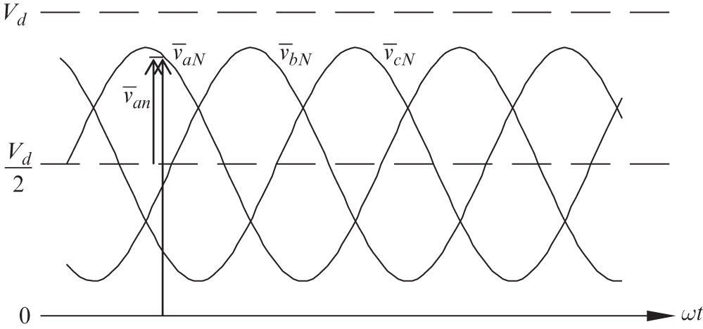
FIGURE 12.27 Switching-cycle-averaged voltages due to sine-PWM.
In Figure 12.27, using Equation 12.3, the plots of ![]() ,
, ![]() , and
, and ![]() , each divided by
, each divided by ![]() , are also the plots of
, are also the plots of ![]() ,
, ![]() , and
, and ![]() within the limits of
within the limits of ![]() and
and ![]() :
:
These power-pole duty ratios define the turns ratio in the ideal transformer representation of Figure 12.25b. As can be seen from Figure 12.27, at the limit, ![]() can become a maximum of
can become a maximum of ![]() and hence the maximum allowable value of the phase-voltage peak is
and hence the maximum allowable value of the phase-voltage peak is
Therefore, using the properties of three-phase circuits where the line-line voltage magnitude is ![]() times the phase-voltage magnitude, the maximum amplitude of the line-line voltage in sine-PWM is limited to
times the phase-voltage magnitude, the maximum amplitude of the line-line voltage in sine-PWM is limited to
12.6.1.1 Switching Waveforms in a Three-Phase Inverter with Sine-PWM
In sine-PWM, three sinusoidal control voltages equal the duty ratios, given in Equation 12.41, multiplied by ![]() . These are compared with a triangular waveform signal to generate the switching signals. These switching waveforms for sine-PWM are shown by an example below.
. These are compared with a triangular waveform signal to generate the switching signals. These switching waveforms for sine-PWM are shown by an example below.
Example 12.6
In a three-phase converter of Figure 12.25a, a sine-PWM is used. The parameters and the operating conditions are as follows: ![]() ,
, ![]() ,
, ![]() volts, and similarly for “b” and “c” phases, and the switching frequency
volts, and similarly for “b” and “c” phases, and the switching frequency ![]() .
. ![]() . At
. At ![]() , calculate and plot the switching waveforms for one cycle of the switching frequency.
, calculate and plot the switching waveforms for one cycle of the switching frequency.
Solution At ![]() ,
, ![]() ,
, ![]() , and
, and ![]() . Therefore, from Equation 12.40,
. Therefore, from Equation 12.40, ![]() ,
, ![]() , and
, and ![]() . From Equation 12.41, the corresponding power-pole duty ratios are
. From Equation 12.41, the corresponding power-pole duty ratios are ![]() ,
, ![]() , and
, and ![]() . For
. For ![]() , these duty ratios also equal the control voltages in volts. The switching time period
, these duty ratios also equal the control voltages in volts. The switching time period ![]() . Based on this, the switching waveforms are shown in Figure 12.28.
. Based on this, the switching waveforms are shown in Figure 12.28.

FIGURE 12.28 Switching waveforms in Example 12.6.
12.6.1.2 Simulation and Hardware Prototyping
The simulation of a three-phase inverter modulated using sine-PWM is demonstrated by means of an example:
Example 12.7
A three-phase inverter is connected to a balanced three-phase ![]() load,
load, ![]() , and
, and ![]() . The DC voltage
. The DC voltage ![]() . The desired output voltage is
. The desired output voltage is ![]() line-line RMS at
line-line RMS at ![]() . Simulate this converter using LTspice.
. Simulate this converter using LTspice.
Solution The simulation file used in this example is available on the accompanying website. The LTspice model is shown in Figure 12.29, and the steady-state waveforms from the simulation of this converter are shown in Figure 12.30.

FIGURE 12.29 LTspice model.
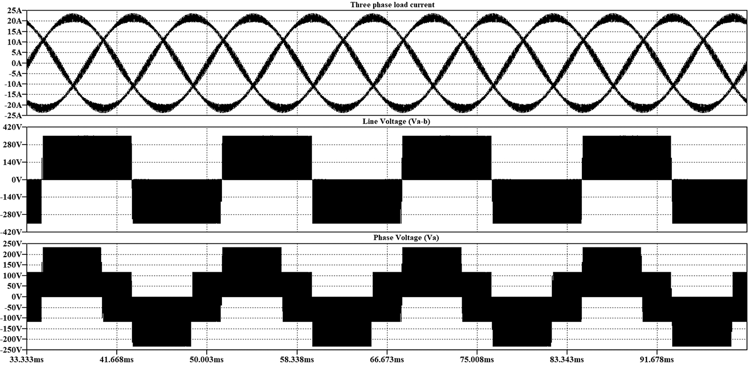
FIGURE 12.30 LTspice simulation results.
The same control algorithm used in Example 12.7 is implemented in Workbench, as shown in Figure 12.31, to generate a balanced three-phase sinusoidal voltage from DC using the Sciamble lab kit.

FIGURE 12.31 Workbench model.
In the hardware, the available DC-bus voltage is ![]() , and this is used to generate a
, and this is used to generate a ![]() RMS,
RMS, ![]() output voltage, as shown in Figure 12.32. The switching frequency is chosen to be
output voltage, as shown in Figure 12.32. The switching frequency is chosen to be ![]() . The step-by-step procedure for re-creating the above hardware implementation is presented in [2].
. The step-by-step procedure for re-creating the above hardware implementation is presented in [2].

FIGURE 12.32 Workbench hardware results: (1) , (2)
, (2)  , (3)
, (3)  , AND (4)
  .
.
12.6.2 Space Vector PWM (SV-PWM)
The use of space vectors has been introduced on a physical basis such that it can be used in teaching the first course dealing with 3-phase AC machines [3]. This approach has numerous benefits compared to conventional methods of understanding AC machines.
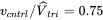
The voltage space vector is a compact way to represent all the three-phase voltages desired at any instant by a single variable. This switching-cycle averaged space vector is synthesized using space-vector PWM (SV-PWM), which fully utilizes the available DC-bus voltage and results in the AC output, which can be approximately 15% higher than that possible by using the sine-PWM approach, both in a linear range, where no lower-order harmonics appear.
Sine-PWM is limited to ![]() , as given by Equation 12.43, because it synthesizes output voltages on a per-pole basis, which does not take advantage of the three-phase properties. Physically, by considering line-line voltages, it is possible to get
, as given by Equation 12.43, because it synthesizes output voltages on a per-pole basis, which does not take advantage of the three-phase properties. Physically, by considering line-line voltages, it is possible to get ![]() in SV-PWM.
in SV-PWM.
12.6.2.1 Definition of Space Vectors
Space vectors can be easily understood by considering a balanced three-phase load, for example, an AC machine, as shown in Figure 12.25, where the a-axis is taken as the reference axis, and the phase axes for the other two phases are ![]() and
and ![]() radians away in the counterclockwise direction.
radians away in the counterclockwise direction.
The stator space voltage vector at any instant is defined as follows, by multiplying the stator phase voltages at that instant by their respective axes’ orientation and summing them:
In terms of the inverter output voltages with respect to the negative DC bus “N” in Figure 12.33, and hypothetically assuming the stator neutral as a reference ground,

FIGURE 12.33 Inverter with a three-phase output.
Substituting Equations 12.45 into Equation 12.44 and recognizing that
the instantaneous stator voltage space vector can be written in terms of the inverter output voltages as
A switch in an inverter pole of Figure 12.33 is in the “up” position if the pole-switching function ![]() and in the “down” position if
and in the “down” position if ![]() . In terms of the switching functions, the instantaneous voltage space vector can be written as
. In terms of the switching functions, the instantaneous voltage space vector can be written as
With three poles, eight switch-status combinations are possible. In Equation 12.48, the instantaneous stator voltage vector ![]() can take on one of the following seven distinct instantaneous values where in a digital representation, phase “a” represents the least significant digit and phase “c” the most significant digit (for example, the resulting voltage vector due to the switch-status combination
can take on one of the following seven distinct instantaneous values where in a digital representation, phase “a” represents the least significant digit and phase “c” the most significant digit (for example, the resulting voltage vector due to the switch-status combination ![]() is represented as
is represented as ![]() ):
):
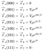 (12.49)
In Equation 12.49, ![]() and
and ![]() are the zero vectors because of their zero value. The resulting instantaneous stator voltage vectors, which we will call the “basic vectors,” are plotted in Figure 12.34. The basic vectors form six sectors, as shown in Figure 12.34.
are the zero vectors because of their zero value. The resulting instantaneous stator voltage vectors, which we will call the “basic vectors,” are plotted in Figure 12.34. The basic vectors form six sectors, as shown in Figure 12.34.

FIGURE 12.34 Basic voltage vectors ( and
and  are not shown).
It should be noted that the basic voltage vectors are the only true instantaneous voltages. However, the machine phase voltages that we are aiming to synthesize, for example, in Equation 12.44, are the switching-cycle-averaged voltages, and therefore, to be rigorous, they should be written as ![]() , and so on
. Therefore, the switching-cycle-averaged space vector in Equation 12.44 will have to be written as
, and so on
. Therefore, the switching-cycle-averaged space vector in Equation 12.44 will have to be written as ![]() . This is not done in the analysis presented here simply to avoid complicating the symbols, but the intent should be clearly understood. Reiterating, as shown in Figure 12.34, the basic vectors are the truly instantaneous space vectors, which by time-weighted averaging called SV-PWM and, as discussed in the next section, allow us to synthesize the space vector
. This is not done in the analysis presented here simply to avoid complicating the symbols, but the intent should be clearly understood. Reiterating, as shown in Figure 12.34, the basic vectors are the truly instantaneous space vectors, which by time-weighted averaging called SV-PWM and, as discussed in the next section, allow us to synthesize the space vector ![]() of Figure 12.34, which is switching-cycle-averaged.
of Figure 12.34, which is switching-cycle-averaged.
12.6.2.2 SV-PWM
The objective of the PWM control of the inverter switches is to synthesize the desired reference stator voltage space vector in an optimum manner with the following objectives:
- A constant switching frequency
 ;
; - Smallest instantaneous deviation from its reference value;
- Maximum utilization of the available DC-bus voltages;
- Lowest ripple in the motor current;
- Minimum switching loss in the inverter.
The above conditions are generally met if the average voltage vector is synthesized by means of the two instantaneous basic nonzero voltage vectors that form the sector (in which the average voltage vector to be synthesized lies) and both the zero-voltage vectors, such that each transition causes the change of only one switch status to minimize the inverter switching loss.
In the following analysis, we will focus on the average voltage vector in sector 1 with the aim of generalizing the discussion to all sectors. To synthesize an average voltage vector ![]() over a time period
over a time period ![]() , as shown in Figure 12.35, the adjoining basic vectors
, as shown in Figure 12.35, the adjoining basic vectors ![]() and
and ![]() are applied for intervals
are applied for intervals ![]() and
and ![]() , respectively, and the zero vectors
, respectively, and the zero vectors ![]() and
and ![]() are applied for a total duration of
are applied for a total duration of ![]() .
.

FIGURE 12.35 Voltage vector in sector 1.
In terms of the basic voltage vectors, the average voltage vector can be expressed as
or
where
In Equation 12.51, expressing voltage vectors in terms of their amplitude and phase angles results in
By equating real and imaginary terms on both sides of Equation 12.53, we can solve for ![]() and
and ![]() (in terms of the given values of
(in terms of the given values of ![]() ,
, ![]() , and
, and ![]() ) to synthesize the desired average space vector in sector 1.
) to synthesize the desired average space vector in sector 1.
Having determined the durations for the adjoining basic vectors and the two zero vectors, the next task is to relate the above discussion to the actual poles (a, b, and c). Note in Figure 12.34 that in any sector, the adjoining basic vectors differ in one position. For example, in sector 1 with the basic vectors ![]() and
and ![]() , only the pole b differs in the switch position. For sector 1, the switching pattern in Figure 12.36 shows that pole a is in “up” position during the sum of
, only the pole b differs in the switch position. For sector 1, the switching pattern in Figure 12.36 shows that pole a is in “up” position during the sum of ![]() ,
, ![]() , and
, and ![]() intervals and hence for the longest interval of the three poles. Next in the length of duration in the “up” position is pole b for the sum of
intervals and hence for the longest interval of the three poles. Next in the length of duration in the “up” position is pole b for the sum of ![]() and
and ![]() intervals. The smallest in the length of duration is pole c for only the
intervals. The smallest in the length of duration is pole c for only the ![]() interval. Each transition requires a change in switch state in only one of the poles, as shown in Figure 12.36. Similar switching patterns for the three poles can be generated for any other sector.
interval. Each transition requires a change in switch state in only one of the poles, as shown in Figure 12.36. Similar switching patterns for the three poles can be generated for any other sector.

FIGURE 12.36 Waveforms in sector 1 ( ).
).
12.6.2.3 Limit on the Amplitude  of the Stator Voltage Space Vector
First, we will establish the absolute limit on the amplitude ![]() of the average stator voltage space vector at various angles. The limit on the amplitude equals
of the average stator voltage space vector at various angles. The limit on the amplitude equals ![]() (the DC-bus voltage) if the average voltage vector lies along a nonzero basic voltage vector. In between the basic vectors, the limit on the average voltage vector amplitude is that its tip can lie on the straight lines shown in Figure 12.37, forming a hexagon.
(the DC-bus voltage) if the average voltage vector lies along a nonzero basic voltage vector. In between the basic vectors, the limit on the average voltage vector amplitude is that its tip can lie on the straight lines shown in Figure 12.37, forming a hexagon.
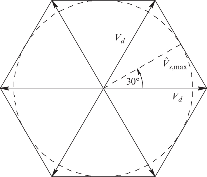
FIGURE 12.37 Limit on amplitude  .
.
However, the maximum amplitude of the output voltage ![]() should be limited to the circle within the hexagon in Figure 12.37 to prevent distortion in the resulting currents. This can be easily concluded from the fact that in a balanced sinusoidal steady state, the voltage vector
should be limited to the circle within the hexagon in Figure 12.37 to prevent distortion in the resulting currents. This can be easily concluded from the fact that in a balanced sinusoidal steady state, the voltage vector ![]() rotates at the synchronous speed
rotates at the synchronous speed ![]() , with its constant amplitude, where
, with its constant amplitude, where ![]() is the frequency of the phase voltages. At its maximum amplitude,
is the frequency of the phase voltages. At its maximum amplitude,
Therefore, the maximum value that ![]() can attain is
can attain is
In a balanced steady state, the peak of the phase voltages is ![]() times the amplitude of the space vector. Therefore, from Equation 12.55, the corresponding limits on the phase voltage and the line-line voltages are as follows:
times the amplitude of the space vector. Therefore, from Equation 12.55, the corresponding limits on the phase voltage and the line-line voltages are as follows:
and
The sine-PWM in the linear range, as discussed before, results in a maximum voltage
A comparison of Equations 12.57 and 12.58 shows that the SV-PWM discussed in this chapter better utilizes the DC-bus voltage and results in a higher limit on the available output voltage by a factor of ![]() , or by approximately 15% higher, compared to the sine-PWM.
, or by approximately 15% higher, compared to the sine-PWM.
Example 12.8
Similar to that in Example 12.6, consider the three-phase converter of Figure 12.21a, where ![]() and
and ![]() volts, and so forth. Obtain the duty ratios
volts, and so forth. Obtain the duty ratios ![]() , using SV-PWM at
, using SV-PWM at ![]() .
.
Solution The voltage space vector at ![]() is obtained using Equation 12.47
:
is obtained using Equation 12.47
:![]()
This is in sector 1 of the voltage vectors shown in Figure 12.34. In sector 1, The two nonzero vectors are ![]() and
and ![]() . The ratio of the switching time period each of these vectors is applied is determined using Equation 12.53:
. The ratio of the switching time period each of these vectors is applied is determined using Equation 12.53:
Solving the above equation gives ![]() and
and ![]() . The two zero vectors
. The two zero vectors ![]() and
and ![]() are shared equally in the remaining period:
are shared equally in the remaining period:
Now the duty cycle of each phase can be obtained by summing up the duty cycles of each vector whose phase’s switch is in the “up” position during that phase: ![]() ,
, ![]() , and
, and ![]() .
.
12.6.2.4 Simulation and Hardware Prototyping
The simulation of a three-phase inverter modulated using SV-PWM is demonstrated by means of an example:
Example 12.9
A three-phase inverter is connected to a balanced three-phase ![]() load, where
load, where ![]() and
and ![]() . The DC voltage
. The DC voltage ![]() . The desired output voltage is
. The desired output voltage is ![]() line-line RMS at
line-line RMS at ![]() . Simulate this converter using LTspice.
. Simulate this converter using LTspice.
Solution The simulation file used in this example is available on the accompanying website. The LTspice model is shown in Figure 12.38, and the steady-state waveforms from the simulation of this converter are shown in Figure 12.39.

FIGURE 12.38 LTspice model.

FIGURE 12.39 LTspice simulation results.
The same control algorithm used in Example 12.9 is implemented in Workbench, as shown in Figure 12.40, to generate a balanced three-phase sinusoidal voltage from DC using the Sciamble lab kit.
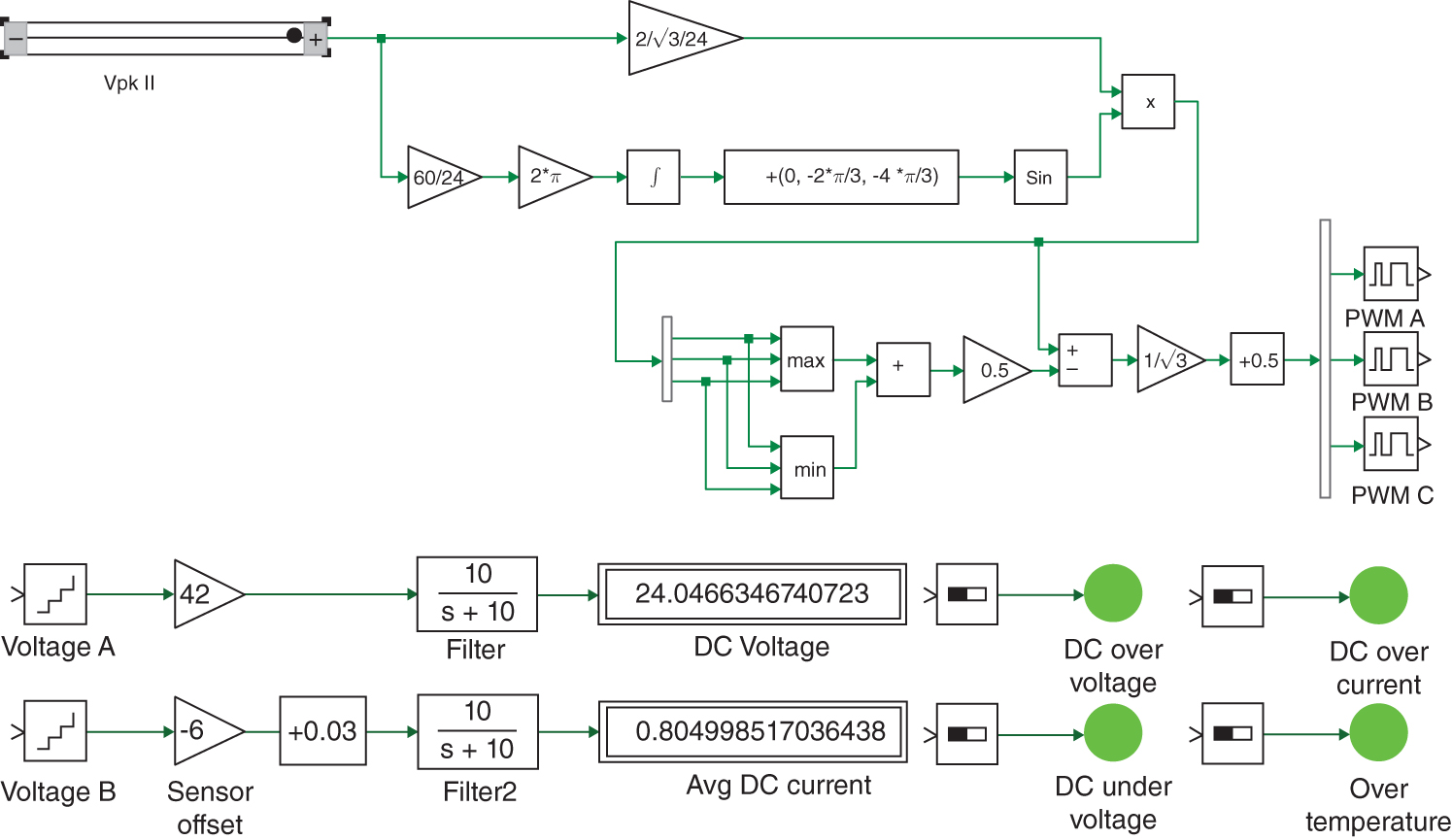
FIGURE 12.40 Workbench model.
In the hardware, the available DC-bus voltage is ![]() , and this is used to generate a
, and this is used to generate a ![]() RMS,
RMS, ![]() output voltage, as shown in Figure 12.41. The switching frequency is chosen to be
output voltage, as shown in Figure 12.41. The switching frequency is chosen to be ![]() . The step-by-step procedure for re-creating the above hardware implementation is presented in [4].
. The step-by-step procedure for re-creating the above hardware implementation is presented in [4].

FIGURE 12.41 Workbench hardware results: (1) , (2)
, (2)  , (3)
, (3)  , AND (4)
  .
.
12.6.3 Over-Modulation and Square-Wave (Six-step) Mode of Operation [5]
So far, in using sine-PWM and SV-PWM, it is assumed that the control voltage peak is kept equal to or less than the triangular waveform peak ![]() . This results in a linear range where the output phase voltages, ignoring the common-mode offset voltages that do not appear across the load, are linearly related to the control voltages. Therefore, in terms of functionality, a PWM converter is similar to a linear amplifier in the linear modulation. In addition to this linearity, the harmonics in the switched output waveform are, as shown in Figure 12.8b, at around the multiples of the switching frequency. That is, the low-order harmonics that are multiples of the low-frequency
. This results in a linear range where the output phase voltages, ignoring the common-mode offset voltages that do not appear across the load, are linearly related to the control voltages. Therefore, in terms of functionality, a PWM converter is similar to a linear amplifier in the linear modulation. In addition to this linearity, the harmonics in the switched output waveform are, as shown in Figure 12.8b, at around the multiples of the switching frequency. That is, the low-order harmonics that are multiples of the low-frequency ![]() (the fundamental frequency) do not appear in the output.
(the fundamental frequency) do not appear in the output.
However, in applications such as motor drives at higher than rated speed, it may be advantageous to get as high a voltage as possible at the fundamental frequency ![]() , even if the output contains harmonics that are low-order multiples of
, even if the output contains harmonics that are low-order multiples of ![]() . This requires the control voltages to exceed the triangular-waveform peak by over-modulation. The output voltage-switching waveform, as a consequence, contains low-order harmonics that can be obtained by Fourier analysis. At the limit, in each switching power-pole, the switch is in “up” position for one-half the time period and “down” for the other half, as shown in Figure 12.42.
. This requires the control voltages to exceed the triangular-waveform peak by over-modulation. The output voltage-switching waveform, as a consequence, contains low-order harmonics that can be obtained by Fourier analysis. At the limit, in each switching power-pole, the switch is in “up” position for one-half the time period and “down” for the other half, as shown in Figure 12.42.

FIGURE 12.42 Square-wave (six-step) waveforms.
The output waveforms of the three poles are displaced by ![]() radians with respect to each other. The resulting output waveforms are square waves, and such an operation is called square-wave or six-step mode of operation. For a given DC-bus voltage
radians with respect to each other. The resulting output waveforms are square waves, and such an operation is called square-wave or six-step mode of operation. For a given DC-bus voltage ![]() , this mode of operation yields the highest possible output voltages at frequency
, this mode of operation yields the highest possible output voltages at frequency ![]() , where by Fourier analysis, at the fundamental frequency,
, where by Fourier analysis, at the fundamental frequency,
which shows that it is possible to get the fundamental-frequency line-line voltage peak greater than ![]() , although at the expense of the low-order harmonic voltages,
, although at the expense of the low-order harmonic voltages,
12.7 MULTILEVEL INVERTERS
In high-power and high-voltage applications, it is desirable to operate with high values of voltages in order to keep the associated currents to manageable levels. This requires the DC-bus voltage ![]() to be large so that it exceeds the voltage ratings of the transistors (of course, a safety margin has to be used), as shown in Figure 12.3a of a switching power-pole. One option in such a case is to use multiple transistors in series in order to yield, effectively, each transistor in Figure 12.3a. This is done in practice; however, great care must be taken to ensure that all the transistors in series switch in unison so that they share voltages equally.
to be large so that it exceeds the voltage ratings of the transistors (of course, a safety margin has to be used), as shown in Figure 12.3a of a switching power-pole. One option in such a case is to use multiple transistors in series in order to yield, effectively, each transistor in Figure 12.3a. This is done in practice; however, great care must be taken to ensure that all the transistors in series switch in unison so that they share voltages equally.
Another option that has been used sometimes is to have a three-level arrangement, as shown in Figure 12.43, where a midpoint “o” is established by two series-connected equal capacitors as shown with equal DC voltages ![]() [4].
[4].

FIGURE 12.43 Three-level inverters.
We will consider the switching power-pole for phase a. By turning switches ![]() and
and ![]() on, with respect to the midpoint, the switching-pole output voltage
on, with respect to the midpoint, the switching-pole output voltage ![]() regardless of the current direction. Turning
regardless of the current direction. Turning ![]() and
and ![]() on results in
on results in ![]() . Similarly, turning
. Similarly, turning ![]() and
and ![]() on results in
on results in ![]() . There are two major advantages of the three-level inverter: (1) transistors in Figure 12.43 need to block only one-half the DC-bus voltage, that is,
. There are two major advantages of the three-level inverter: (1) transistors in Figure 12.43 need to block only one-half the DC-bus voltage, that is, ![]() , without the need to connect two transistors in series and without the associated problem of ensuring equal voltage sharing mentioned earlier, and (2) three levels (
, without the need to connect two transistors in series and without the associated problem of ensuring equal voltage sharing mentioned earlier, and (2) three levels (![]() , 0,
, 0,![]() ) result in less switching-frequency ripple in the output for the same switching frequency, as compared to two-level inverters discussed earlier. One of the drawbacks of these inverters is the need to ensure that the midpoint remains at half the DC bus voltage.
) result in less switching-frequency ripple in the output for the same switching frequency, as compared to two-level inverters discussed earlier. One of the drawbacks of these inverters is the need to ensure that the midpoint remains at half the DC bus voltage.
Multilevel inverters with more than three levels have been reported in the literature with various advantages and challenges [6, 7]. A detailed discussion of this topic is presented in [8].
12.8 CONVERTERS FOR BIDIRECTIONAL POWER FLOW
In many applications, the power flow through the voltage-link structure of Figure 12.1 is bidirectional. For example, in motor drives, normally, power flows from the utility to the motor, and while slowing down, the energy stored in the inertia of machine-load combination can be recovered by operating the machine as a generator and feeding power back into the utility grid. This can be accomplished by using three-phase converters, discussed in section 12.6, at both ends, as shown in Figure 12.44a, recognizing that the power flow through these converters is bidirectional.

FIGURE 12.44 Voltage-link structure for bidirectional power flow.
In the normal mode, the converter at the utility-end operates as a rectifier and the converter at the machine-end as an inverter. The roles of these two are opposite when the power flows in the reverse direction during energy recovery. A similar arrangement can be used in connecting two AC systems by means of a HVDC transmission line.
The switching-cycle-averaged representation of these converters by means of ideal transformers is shown in Figure 12.44b. In this simplified representation, where losses are ignored, one side is represented by a source ![]() , and so forth, in series with the internal system inductance
, and so forth, in series with the internal system inductance ![]() . The other side, for example, an AC machine, is represented by its steady-state equivalent circuit, the equivalent machine inductance
. The other side, for example, an AC machine, is represented by its steady-state equivalent circuit, the equivalent machine inductance ![]() in series with the back-emf
in series with the back-emf ![]() , and so on. Under balanced three-phase operation at both ends, the role of each converter can be analyzed by means of the per-phase equivalent circuits shown in Figure 12.44c. In these per-phase equivalent circuits, the fundamental-frequency voltages produced at the AC side by the two converters are
, and so on. Under balanced three-phase operation at both ends, the role of each converter can be analyzed by means of the per-phase equivalent circuits shown in Figure 12.44c. In these per-phase equivalent circuits, the fundamental-frequency voltages produced at the AC side by the two converters are ![]() and
and ![]() , and the AC-side currents at the two sides can be expressed in the phasor form as
, and the AC-side currents at the two sides can be expressed in the phasor form as
where the phasors in Equation 12.61 represent voltages and current at the frequency ![]() of side 1 and the phasors in Equation 12.62 at the fundamental-frequency
of side 1 and the phasors in Equation 12.62 at the fundamental-frequency ![]() synthesized at side 2.
synthesized at side 2.
In Figure 12.44a, for a given utility voltage, it is possible to control the current drawn from side 1 by controlling the voltage synthesized by the side 1 converter in magnitude and phase. In these circuits, if the losses are ignored, the switching-cycle-averaged power drawn from side 1 equals the power supplied to side 2. However, the reactive power at the side 1 converter can be controlled independently of the reactive power at the side 2 converter.
12.9 MATRIX CONVERTERS (DIRECT LINK SYSTEM)
To review once again, power electronics systems are categorized as voltage-link systems described so far, where a capacitor is used in parallel with two converters as an energy storage element, and current-link systems, described in Chapters 13 and 14, used in very high-power applications, where an inductor is used in series with the two converters for energy storage. There is another structure called the matrix converters, which provides a direct link between the input and the output without any intermediate energy storage element. There is a great deal of research interest at present in these converters because they avoid the intermediate energy storage element.
Such a system for a three-phase to three-phase conversion is shown in Figure 12.45, where there is a bidirectional switch from each input port to each output port. Such a bidirectional switch must be capable of blocking voltages of either polarity and conduct current in either direction. Such a bidirectional switch can be realized, for example, by two IGBTs and two diodes, as connected in Figure 12.45. When the two transistors are gated on, the current can flow in either direction, effectively representing the closed position of the bidirectional switch. When both transistors are gated off, current cannot flow in either direction, effectively representing the closed position of the bidirectional switch. A detailed discussion of this topic is presented in [8].

FIGURE 12.45 Matrix converter.
REFERENCES
- 1. “Single-Phase Inverter Lab Manual.” https://sciamble.com/resources/pe-drives-lab/basic-pe/single-phase-inverter.
- 2. “Sine PWM Lab Manual.” https://sciamble.com/resources/pe-drives-lab/basic-pe/sine-pwm.
- 3. N. Mohan and S. Raju, Analysis and Control of Electric Drives: Simulations and Laboratory Implementation (New York: John Wiley & Sons, 2020).
- 4. “Space Vector PWM Lab Manual.” https://sciamble.com/resources/pe-drives-lab/basic-pe/svpwm.
- 5. N. Mohan, T.M. Undeland, and W.P. Robbins, Power Electronics: Converters, Applications and Design, 3rd Edition (New York: John Wiley & Sons, 2003).
- 6. J. Rodríguez, et al., “Multilevel Inverters: A Survey of Topologies, Controls, and Applications,” IEEE Transactions on Industrial Electronics 49, no. 4 (August 2002): 724–738.
- 7. V.T. Somasekhar, K. Gopakumar, M.R. Baiju, K.K. Mohapatra, and L. Umanand, “A Multilevel Inverter System for an Induction Motor with Open-End Windings,” IEEE Transactions on Industrial Electronics 52, no. 3 (June 2005), 824–836.
- 8. N. Mohan, W. Robins, T. Undeland, and S. Raju, Power Electronics for Grid-Integration of Renewables: Analysis, Simulations and Hardware Lab (New York: John Wiley & Sons, 2023).
PROBLEMS
Switching Power-Pole
- 12.1 In a switch-mode converter pole a,
 ,
,  , and
, and  . Calculate the values of the control signal
  and the pole duty ratio
  during which the switch is in its top position, for the following values of the average output voltage:
  and
and  .
. - 12.2 In a converter pole, including the ripple in the
 waveform, show that the relationship between the currents on both sides of the switching-cycle-averaged power pole is similar to that in an ideal transformer.
DC-MOTOR DRIVES
- 12.3 A switch-mode DC-DC converter uses a PWM-controller IC that has a triangular waveform signal at 25 kHz with
 = 1.5 V. If the input DC source voltage
  , calculate the gain
  in Equation 12.19 of this switch-mode amplifier.
 - 12.4 In a switch-mode DC-DC converter,
 with a switching frequency
  and
and  . Calculate and plot the ripple in the output voltage
  .
. - 12.5 A switch-mode DC-DC converter is operating at a switching frequency of 20 kHz, and
 = 150 V. The average current being drawn by the DC motor is 8.0 A. In the equivalent circuit of the DC motor,
  ,
,  , and
, and  . (a) Plot the output current and calculate the peak-to-peak ripple, and (b) plot the current on the DC side of the converter.
 - 12.6 In Problem 12.5, the motor goes into regenerative braking mode. The average current being supplied by the motor to the converter during braking is 7.0 A. Plot the voltage and current waveforms on both sides of this converter at that instant. Calculate the average power flow into the converter.
- 12.7 In Problem 12.5, calculate
 ,
,  , and
, and  .
. - 12.8 Repeat Problem 12.5 if the motor is rotating in the reverse direction, with the same current draw and the same induced emf
 value of the opposite polarity.
 - 12.9 Repeat Problem 12.8 if the motor is braking while it has been rotating in the reverse direction. It supplies the same current and produces the same induced emf
 value of the opposite polarity.
 - 12.10 Repeat Problem 12.5 if a bipolar voltage switching is used in the DC-DC converter. In such a switching scheme, the two bi-positional switches are operated in such a manner that when switch a is in the top position, switch b is in its bottom position, and vice versa. The switching signal for pole a is derived by comparing the control voltage (as in Problem 12.5) with the triangular waveform.
SINGLE-PHASE INVERTERS
- 12.11 In a 1-phase UPS,
 ,
,  , and
, and  . Calculate and plot
  ,
,  ,
,  ,
,  ,
,  ,
,  , and
, and  . Switching frequency
  .
. - 12.12 In Problem 12.11, calculate
 and
and  at
at  .
.
THREE-PHASE INVERTERS
- 12.13 Plot
 if the output voltage of the converter pole a is
 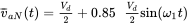 , where
  .
. - 12.14 In a three-phase DC-AC inverter,
 ,
,  , the maximum value of the control voltage reaches
  , and
, and  . Calculate and plot (a) the duty ratios
  ,
,  ,
,  , (b) the pole output voltages
  ,
,  ,
,  , and (c) the phase voltages
  ,
,  , and
, and  .
. - 12.15 In a balanced three-phase DC-AC converter, the phase a average output voltage is
 , where
  and
and  . The inductance
  in each phase is 5 mH. The AC motor internal voltage in phase A can be represented as
  . (a) Calculate and plot
  ,
,  , and
, and  , and (b) sketch
  and
and  .
. - 12.16 In Problem 12.15, calculate and plot
 , which is the average DC current drawn from the DC side.
 - 12.17 In a converter
 . To synthesize an average stator voltage vector
  , calculate
  ,
,  , and
, and  .
. - 12.18 Given that
 , calculate the phase voltage components.
SIMULATION PROBLEMS
- 12.19 Simulate a single-phase inverter where
 , the output voltage
  is 150 V (RMS) at the fundamental frequency, which is 45 Hz. The output current
  has an RMS value of 10 A at a lagging power factor of 0.866. The switching frequency is
  . The output load can be simulated by a back-emf in series with a resistance of
  and an inductance of
  .
.- Obtain
 and
and  waveforms.
 - By Fourier analysis, obtain
 , and plot the
  and
and  waveforms.
 - Obtain the
 waveform.
 - By Fourier analysis, obtain
 and
and  , and plot them.
 - Obtain the RMS value of the high-frequency ripple current in
 .
.
- Obtain
- 12.20 In the single-phase inverter of Problem 12.17, represent each of the two poles by their average model.
- Obtain the
 and
and  waveforms.
 - Obtain the
 waveform.
 - Obtain
 and
and  , and plot them.
- Obtain the
- 12.21 Simulate a three-phase inverter where
 , the output voltage
  is 175 V(RMS) at the fundamental frequency, which is 45 Hz. The output current has an RMS value of 10 A at a lagging power factor of 0.866. The switching frequency is
  . The per-phase output load can be simulated by a back-emf in series with a resistance of
  and an inductance of
  .
.- Obtain the waveforms for
 (with respect to load-neutral),
  and
and  .
. - Obtain
 by means of Fourier analysis of the
  waveform.
 - Using the results of part (b), obtain the ripple component
 waveform in the output voltage.
- Obtain the waveforms for
- 12.22 In the three-phase inverter of Problem 12.19, represent each of the three poles by their average model.
- Observe the waveforms for
 ,
,  , and
, and  .
. - Append the output current waveforms of the switching model of Problem 12.19.
- Observe the waveforms for