

Complex prototype missing a single wire
Now of course you can fix these issues with your prototype; just reconnect, replace, fiddle, and so on, and it will be back and working in no time. Remember, way back in the first part of the book I said the key thing that smart devices do is enable functionality without babysitting? That’s why breadboards are lousy for “production”, because they need to either never be touched or require constant babysitting. So how do you fix this issue and move beyond prototype into something more permanent? The great news is there are lots of ways you can do this, and we will discuss the most simple and likely solutions in the next couple of chapters on the way to permanence.
Locking It Down
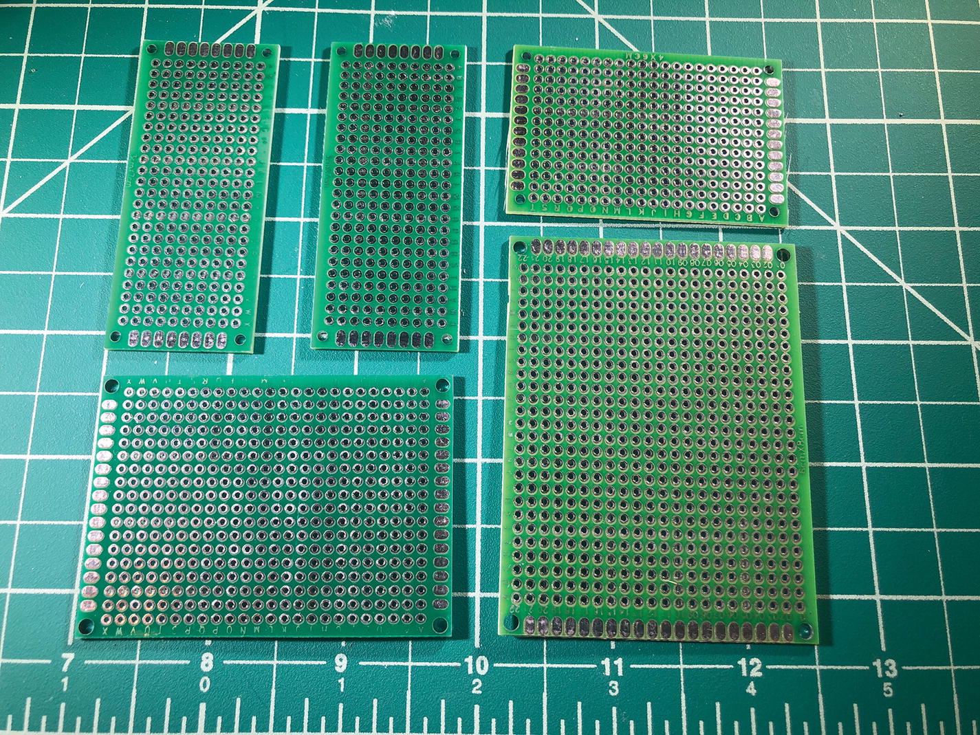
Solderable breadboards
You can solder your jumper wires, chips, MCU, really anything with a through-hole mount, which is pretty much everything you are likely to encounter unless you are getting into some of the more exotic, circuit board–specific components, and we will talk about that in the next chapter. This attachment provides a semi-permanent (it can be removed) connection that won’t fall apart the second you pick it up or drop it. It can even be mounted to another surface with standoffs through those holes in the corners and made something akin to a permanent device. As you get into testing a prototype this is a great way to be able to test devices “in the field” without spending money on PCBs upfront.
This of course indicates that you will need to solder, and soldering is a skill that when you want to move beyond prototypes rapidly becomes mandatory. Soldering is one of those “barrier to entry” skills that is VERY daunting to people, as there is heat, and multiple parts, and lots of things to learn about it as a discipline by itself. The thing I will tell you is that soldering is actually really a great skill to have, fun to do, and is not as hard as it seems at first with some good prep and proper tools to make things smoother.
The most important thing to remember is, of course, soldering irons get HOT, and they burn. I have several nicks and scars from mine, and it stings like the dickens. That said, I have soldered many thousands of connections with my trusty pen soldering iron, and I rarely give myself any mementos of the experience anymore. Just have a little respect for your kit and the heat, and soldering can be a great experience.
- 1.
Soldering iron with a temp control – You will want to control temperatures! In the olden days, only very high-end machines had this, but now even basic ones have a little dial that gets the job done.
- 2.
Desoldering tool – This is a nifty little vacuum tool that plucks hot solder off your parts. You WILL need this; you will mess up and put too much solder on and this is how you remove it.
- 3.
Tip tinner and cleaning “pod” – Tip tinner is like “non-stick coating” for the soldering iron, and the cleaner “pod” is a metal pod with a steel wool–like bundle in it that is made of brass. This is for cleaning off excess solder from the tip of your iron.
- 4.
Soldering tips – Like paintbrushes for the artists out there, solder tips come in specific shapes for specific sorts of tasks, fine point, wedge, big fat tips, and others. You won’t always use all of them, but having a variety is super helpful.
- 5.
“Helping hands” aka the part holder – This little (or big – there are some crazy complex versions out there!) is invaluable. Soldering is hard when you are trying to hold four things at once, and the helping hands (and magnifying glass) make holding and seeing what you are soldering MUCH easier.
- 6.
Soldering stand – A simple little coil of wire on a metal base that is literally hugely important and useful. It means you can set the iron down without setting your workspace on fire!
- 7.
Solder – Here’s the great news, a big ole spool of this costs a few bucks and lasts forever if you are not at commercial scale. Readily available at big box hardware stores and online.
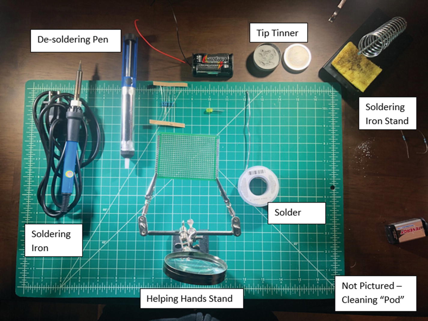
Soldering kit parts
Soldering is such a core competency that learning how to do it is pretty much a basic requirement for making. There is no way a wearable for something like a cosplay prop or a costume, or something that moves like a drone or robot is ever going to hold up without more permanent means of making connections. Breadboards are way too finicky and the connections to fragile for something that needs that level of security in its connections.
Soldering tips wear out, no matter how much you baby them. They are meant to and will eventually need replacement. They are inexpensive to replace but doing so will save you a huge amount of headache, as they can make soldering very difficult when badly worn.
I recommend the brass “sponge” cleaning pod over the damp sponge that comes with most kits. The interaction of the hot and cold will cause the tip to wear out faster. It is worth the few extra bucks to keep things operating smoothly.
Soldering stations are COOL, and you might need one eventually. A pen-style soldering iron is ready to go in a few seconds and will get the job done unless you are soldering many thousands of connections – a really nice kit is available online for around $30. Way better for getting started than a $300 station that you might not use a lot!
Always have a soldering iron stand, always. It looks so simple, but it is so important. You will need to set the iron down and it WILL burn the heck out of everything!
DO NOT BUY/USE COPPER PIPE SOLDER BY MISTAKE – I have a “friend” who did this once. That friend is me, I did it, and it destroyed the tip and the component and the board, and there was great sadness.
DO get lead-free solder with a rosin core (this is what you will find most readily online and in stores if you are not looking in the pipe solder section).
Make sure you solder in a well-ventilated area – you don’t need a big air mover and all that, but do step away for a few minutes as the fumes and smoke can have nasty stuff in them. A small fan isn’t a terrible companion to your bench while soldering.
Clean up your workspace and yourself after soldering – wash your hands really well with soap and water as solder can leave residue.
Lay down some paper or other disposable covering on your workspace – solder will spatter here and there, and the rosin and other coating materials from boards can also drip and it will damage desks and benches
Tin the tip before you start a new soldering session, and frequently during your sessions. You will have a much better soldering experience as it will keep solder flowing cleanly and also gives you a chance to examine the tip for damage.

A soldered connection – the top is before soldering and the bottom is after
Functionally, there isn’t a “right” or “wrong” way to solder such as “only touch the pad” or “only touch the wires.” You will undoubtedly read in other places that one way or the other is better, but in the spirit of just making this easy for everyone, the right way to solder is the one that you are comfortable with and makes nice connections!
I generally prefer to almost “paint” with the solder, by touching the iron to the solder and then flowing it into where I want it like paint on a brush. You can also heat the connection pad where the solder will go, and then touch the solder to that area, but I find this to be unwieldy for me, and doesn’t always give me the connection I want. Ultimately, you should take a solderable board and a few “disposable” components and just practice by soldering and removing them. You can always pull the solder out and remove the component, and in doing so you won’t ruin it. Then you can just use it again, and this will help you get the feel for what technique lets you make good connections.

Good vs. bad solder joints
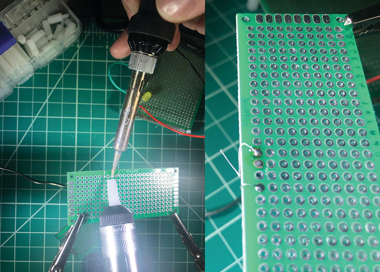
Cleanup of bad connection on the left and after image on the right
The other common thing that can happen is scorching of the circuit board surface. This happens and it is OK! No real damage is done there, other than the discoloring of the surface of the board. (You can see it on the right-hand side of Figure 11-6, around the spot I cleaned up) There isn’t really anything you can do to clean this up, but again, no damage really done, so it’s fine to just leave it. Really the only thing that makes a solder joint “bad” is just that it has too much solder and has bled into something next to it, and those are the ones you need to clean up. Now it is possible that you can overdo it and burn through the PCB material and affect the traces inside on a manufactured board. This is obviously BAD, and you may have damaged the board to the point of being unusable, but you generally need to really leave the iron on it a long time for this. Just double check that you’ve not melted away the material from anything.
It is worth mentioning the other type of solder mistake here that can occur, which is the “cold solder” joint. This occurs when the solder is not really hot enough to fully melt into the joint and form a nice bond. It is very hard to see these types of joints, because the surface will often look like a good solder joint, but underneath it will not have melted and flowed into place. These types of joints can be cleaned up in the same way as my messy solder job earlier, and replaced with a fresh joint, but in a larger project they may cause unintended damage if they fail. The key is to make sure that if you allow your tip to cool for any reason, that you make sure it is hot enough for good solder flow before you start again.
Maintaining Good Iron
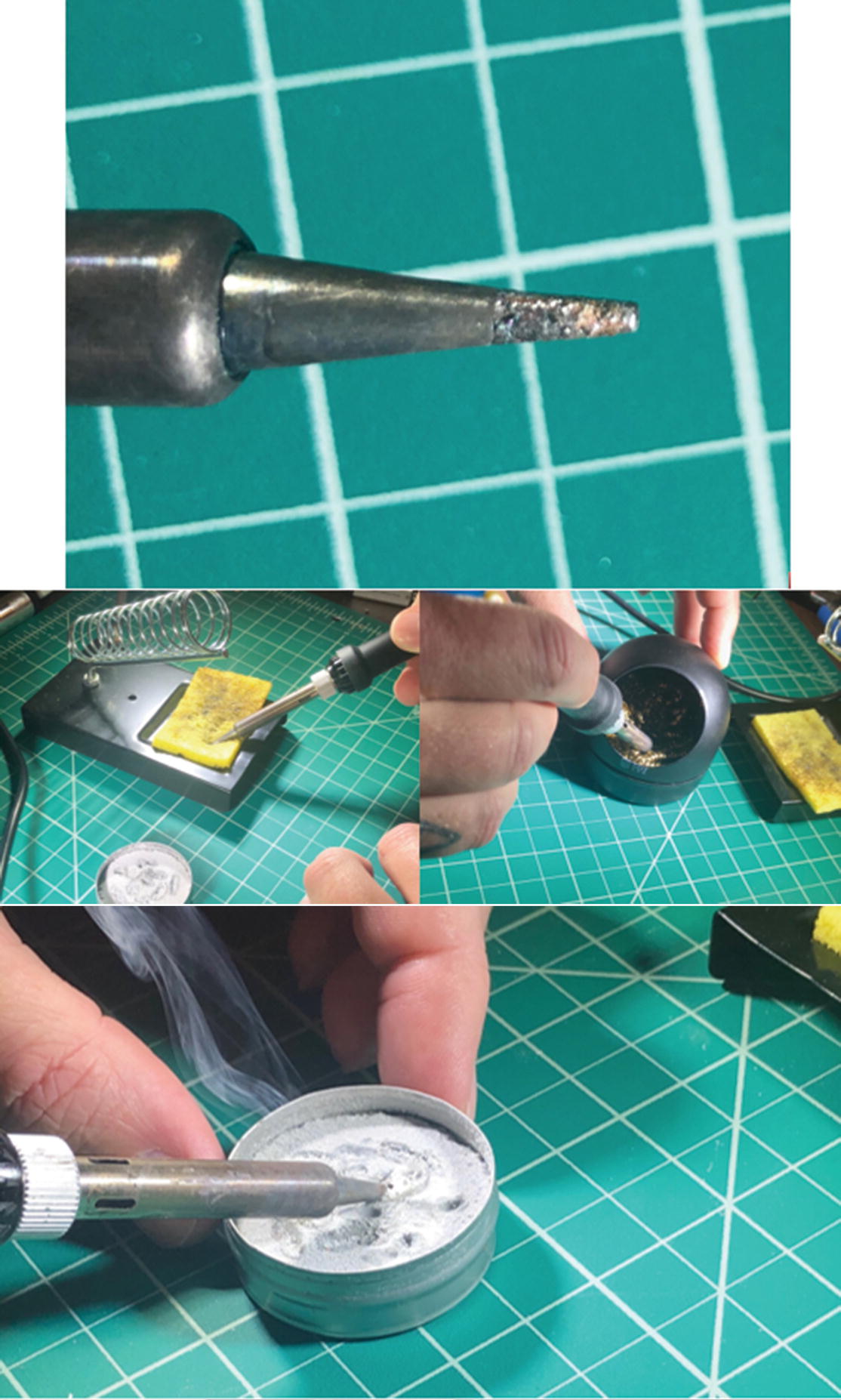

Tip tinning steps
First picture – A “bad” tip. Notice how pitted and scored it is; it needs to be cleaned up and tinned again to work better.
Second picture (left) – Prep the tip for tinning by giving it a nice wipe-off with your wet sponge.
Third picture (right) – A pass through the bronze pad in your cleaning pod removes old tin and gets the tip ready for the tinning.
Fourth picture – Into the tinning material; you don’t need it in here too long, as soon as I see some “smoke” rising I pull it out.
Fifth picture – One more solid wipe with the sponge to remove excess tinning material (you can see the little blob on the sponge).
Last picture – A nice cleaned and tinned tip; notice how all the scoring and roughness is now smoothed and the tip looks much better; that is a good tip!
Cleaning the iron is also important, and you will find that even with a good tin coating, there are still clumps and excess. The default for this is to use the little sponge (get it wet with cool water) that comes with the iron holder usually. I recommend against this for frequent cleanings, as it can accelerate the tip’s degrading because of the expansion and contraction with hot and cold. The brass sponge cleaning pod is much better as it will not cause the tip to change temp, and also more efficiently scrapes off the excess solder. When you find you have clumps, just stab and drag – stab the tip into the brass sponge and drag it out while twisting, and it will scrape off the excess. The only time I generally favor the wet sponge is when I am going to re-tin the tip, because it takes more of the oxidization off than the brass does. Having both is never a bad thing, and you will find the one that gives you the best result as you practice.
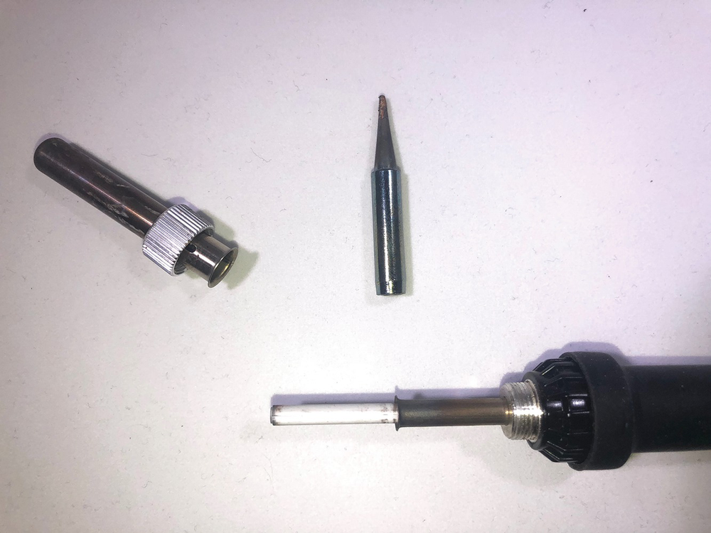
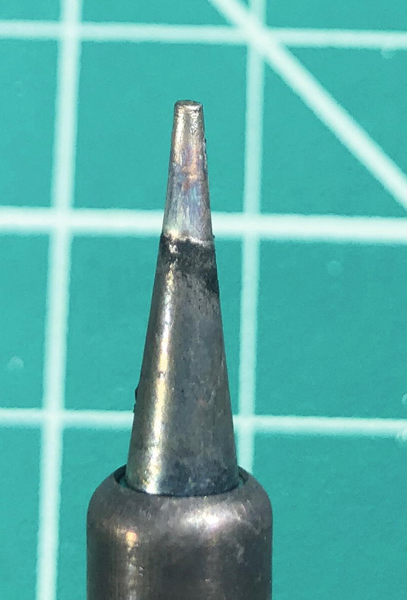
Iron with tip removed
In the lab later I have a couple of practice soldering exercises that will give you a chance to solder, remove, and refine your technique a bit. I highly recommend doing them a few times as they will give you the chance to refine your skills a little before you tackle making your first circuit board using the protoboards. Once you have the hang of it, soldering will be like Ohm’s law, just another part of the process that you are comfortable with and ready to use. This is important, because it’s almost time to make your first circuit board!
Semi-permanent
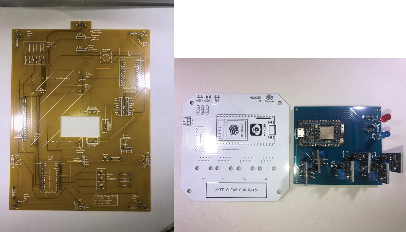
Some PCBs I have designed
Instead of leaping directly to a fully manufactured PCB, there is a nice interim which is to essentially make your own using solderable breadboards. It is because of the permanence and what it means that I have opted to even take this path with you to build what is essentially another prototype. This “middle ground” lets you validate your prototype with solid connections that won’t accidentally get removed through use, and to make sure that nothing in your design is wrong before it’s all made up of permanent connections. This will let you test your device in a more stand-alone way as the last step before going to a full PCB, which we will in the next chapter.
In fact, this is often the stopping point for many devices that you might make for your own use. The reality is that once it has solid connections, and the ability to be put into a more rugged container such as an electrical box or even something you may have 3D printed, the reality is that you have made a permanent device. A full PCB isn’t a requirement of functionality, it is a convenience ultimately, and something that makes mass replication possible at all really, but isn’t strictly required for a device to be considered “field ready” as it were. The protoboard or solderable breadboard is a more than functional means of making something work for a prototype or even a few devices that you are using to validate concepts without the inconvenience of the fragile breadboard. These solderable boards are an effective platform in their own right for this type of prototype exercise and you may only wish to move on to a full PCB when you get to the point of mass replication.

Side-by-side of protoboard and breadboard for the same circuit
For something more complex, or just bulkier, you may find it easier to break parts up into smaller boards. Protoboards come in so many possible sizes that this is also relatively easy to accomplish by selecting the right size protoboard. For example, you might choose to put the sensor on a small board along with any resistors or other small components that need to connect to support the sensor. Then you can connect that via a wire to the board with the MCU on it to conserve some space on that board for connecting devices. Our multi-sensor I2C chip, for example, would be good to mount on its own board with connections to the MCU via the surface pads. This would also make it more “portable” if you decided to swap MCUs, for example.
The nicest element of using the protoboard for your first PCB is undoubtedly that while it is permanently connected up, it can be removed. You can heat up the solder to liquid again and remove the component and move it around or change it all together. This semi-permanence is really important because once you move beyond the prototype to a full PCB, you are now bound by the board. I and many I know have had to replace entire boards, make very ugly patch jobs, or simply start again because of a design flaw with a PCB. Prototyping on the solderable just gives you one more way to make sure it’s all right before you take the leap into the PCB itself.
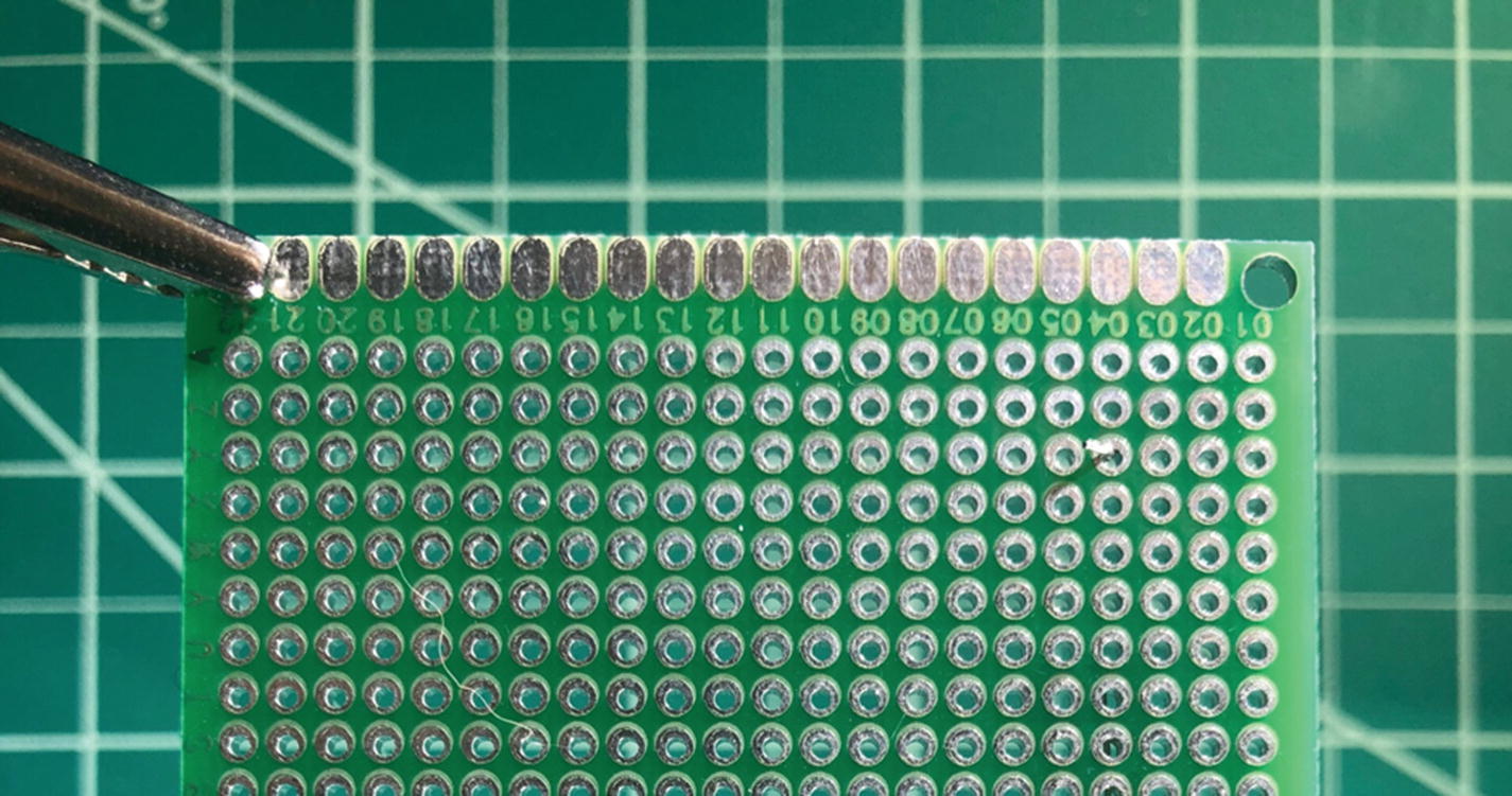
Close-up of solderable breadboard
The surface pads are a nice way to connect external things like our battery packs from previous chapters to the board or even other boards to one another. This particular protoboard is “two sided”; it means that the metal on the “top” and “bottom” of the board does not connect through the board. This is important because of two reasons: this gives you “layers” and is incredibly important when you get to the PCB world in the next chapter (through holes go through layers!), and it means you can make your circuits on the top and the bottom and they will be separate. This in effect means you have a two-layer circuit board, which is great for flexibility, but something to be aware of because you could inadvertently connect the wrong thing, or not make a connection you thought you had. Also, a connection that passes through the hole, such as the pin on a device, definitely will connect the top and bottom layer since the solder will flow into the space and make the connection. This means you can connect to the top and bottom of a device going through the holes on the board.
This concept of layers is something that we will cover in much more depth in the next chapter, but for now, the most important thing to understand is that when connections between parts must cross, they need to be on a separate layer. You have two to work with and so you can probably make some pretty complex circuits, but you will eventually hit a roadblock where two is just not enough layers. It is at that point that you will need to get into multi-layer boards. Again, we will talk about that in more depth later, and the examples for the lab are steered clear of anything that would need more than two layers. If your prototype is complex, however, this might lead to you needing to break out sections of the overall device onto separate protoboards and is just something to be aware of as you start translating your wiring diagrams into the 3D space of the circuit board.

Completed (if ugly) circuit. The back-side solder connections on the left and front-side connections on the right
I am going to give you a walkthrough of soldering up your first circuit, using a simple LED and battery pack just like we did in the first build lab. Now though, you do not need to worry about moving it around and having an LED disconnect or pulling out the wires. As much as it may not seem like it at first, you can actually build some really complex circuits on a protoboard and create some really cool layouts. This interim step is really important for understanding things like routing and layers and can really help you determine how hard or simple your final PCB will be.
Melted out perfboard from solder trace attempt

Standoffs on protoboard
So, as you can see from this, back to my original point about the circuit board you make from a protoboard vs. a PCB that is fully manufactured, there is no real way you are going to mass-produce this. Making all the traces out of solder is messy, and error prone, and frankly just a lot of work. That’s what the PCB itself is for, and why I cover it in the next chapter. You will probably want to make one eventually, if for no other reason than you want more than one or two of the same devices. In the prototype phase though, the handmade circuit will provide you with a platform that is just permanent enough with the stability of solid connections to validate your idea.
Your First Circuit Board Lab
We are going to revisit the basic LED circuit we built in the first section, and I will walk you through building out that most time-honored tradition of “Hello World” by lighting an LED on a semi-permanent protoboard circuit.
Protoboard (I used a big one, but any size is fine; there are not enough connections here to worry about pin counts or spacing.)
68Ohm resistor minimum – I have used a 100Ohm resistor here.
LED (I used yellow because I hadn’t yet in the book, but any color is fine)
One MM wire (left out of the picture – remember this can be any connector; I have used the MM wire for convenience)
3V battery pack (two AA pack)
Soldering kit

The completed circuit with LED lit

Picture of basic circuit parts

Board in hands ready to go

The left is the “front” of the board, and the right shows the pins bent through the “back” to hold the elements for soldering

pins folded down and soldered in place
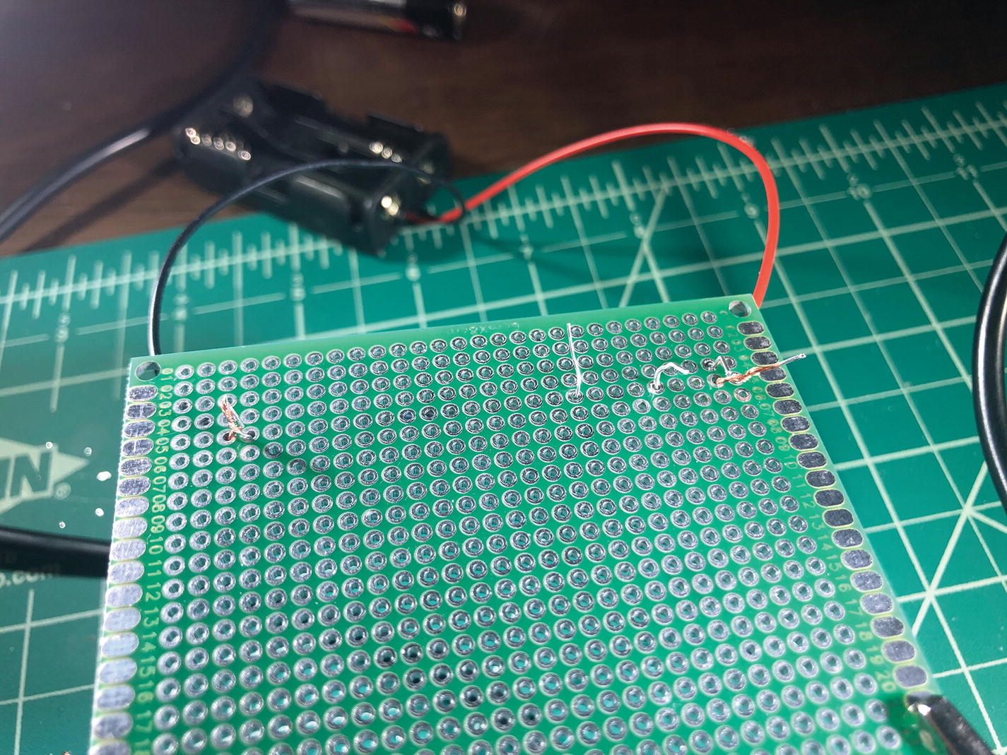
Leads from the battery case passing through the breadboard

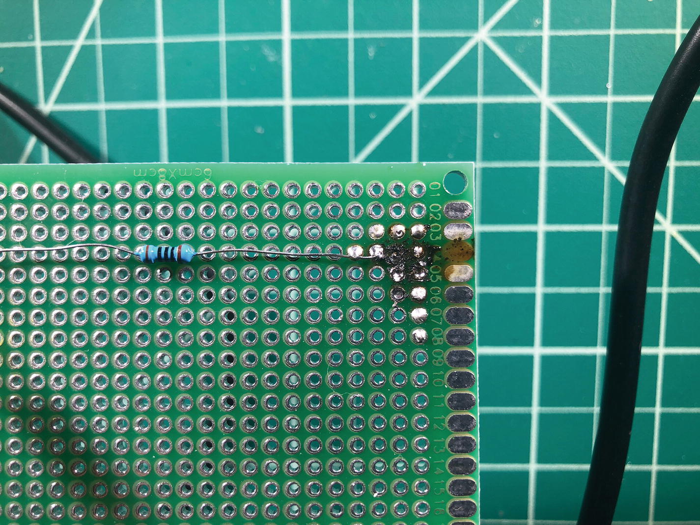
The top shows the “front view” and the bottom is the detail of the completed black wire to resistor connection

Front view of MM wire in place
MM wire pin soldered to board near LED pin

Both MM pins through and soldered to LED and resistor, respectively
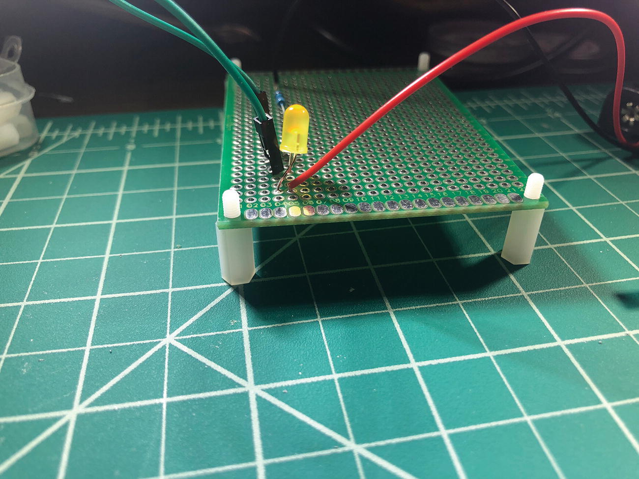
Standoffs in place to support the protoboard

HELLO WORLD!
To assemble the hardware circuit, there are a couple of tips I want to give you. As a novice, the temptation is to try and “rig up” the whole circuit first and then solder it all at once. You CAN do this, BUT it often ends in frustration because gravity is annoying, and pins fall out of their hole and you end up faffing about to get everything in place. The less frustrating way is to solder the pieces on one at a time, get them attached to the board (a single pin will do this) and THEN worry about the connections. I have used this method (minus a couple of opportunities to do things at the same time) in this walkthrough. It is not the ONLY way, and maybe not even the BEST way, but it does avoid a lot of “dang it, where did that PIN go!?”
Right, so let’s build this out!
- 1)
Start by plugging in your iron and setting it to the recommended temp, and then while it heats up, putting your protoboard in your helping hands, if you have them – if not, you can set the board down after you put the pins through the holes, and gravity becomes an ally holding the board to the element. See Figure 11-17 for how this looks.
- 2)
We will start by putting the LED and resistor through the holes to position them for soldering (make sure to check the anode side of your LED – you can flip it around later, but it is more work with solder!). You can do them one at a time if you prefer, but because we can bend the pins to hold them, doing them both is a little timesaver. Figure 11-18 shows both elements in place through their respective holes – pins bent to hold them in place.
- 3)
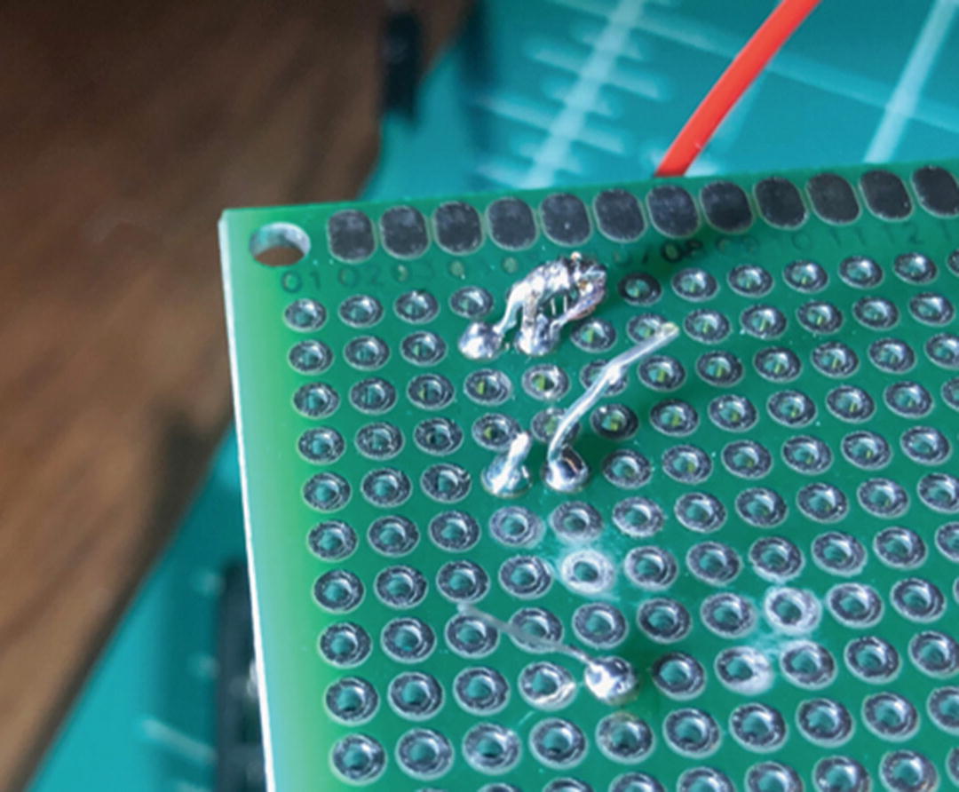
Next we simply solder those four connections. Figure 11-19 shows the finished product, and just remember that a little solder will make a nice connection. Putting on too much will make a blob on the other side of your board you have to clean up later.
- 4)
Now that those connections are set, clean your iron and put it in the stand, and then put the wires from the battery box through their holes. I stripped off some extra on the wire to make this easier and would recommend for you to do the same. Tip: Wrap the wires around the pins for a better hold before you solder! Make sure the black wire is on the resistor end, and the red is on the LED end as in Figure 11-20.
- 5)
As before, you will solder the wire into its respective hole, and then put a bit of solder on the wire and pin from the LED and resistor. Figure 11-21 shows the soldered connection of the black wire in detail so you can see what the connections should look like in place.
- 6)
Clean and park your iron in the stand, and you only have one last connection! Take the MM wire, which will form the last connection between the resistor and LED, and put the pins through holes next to the respective pins you want to connect, as in Figure 11-22. Tip: Bend the pins from the LED and resistor to be close to the MM wire pins, for easier connecting.
- 8)
One last thing to do, but first park your iron back in its stand, and unplug it for safety!! If you have some standoffs, you should put one in each of the four corner holes. While this is not explicitly required, and the voltages so low that you are unlikely to damage anything, it is safer for your circuit. If you have a metal workbench, you for sure need this! You can see what this looks like in Figure 11-25. It just holds the connections above the “ground” so that they don’t touch and potentially short out.
Last step is to put the batteries in the box, and the LED should come on like in Figure 11-26. Congratulations, you have made your first “permanent” circuit. You can pick it up, move it, turn it over, and aside from dropping or throwing it, you should have nice solid connections that will stay put.
- 1.
Did you connect the battery pack wires the right way? If not, you can heat the solder and pull them off and change them around.
- 2.
Pull the LED off and spin it around by heating the solder and pulling the LED out of the holes one at a time, back and forth to work it out.
- 3.
Check that your solder connections are sound and not shorted.
Where to Next?
Well, this was a tough one for me too as I worked on the book and thought through your path as a learner. We started with the basics, some history, and then the electronics and components that make circuits work. We went on to the software side and worked through some of the parts of the smart system and highlighted some easy ways to get you started on the path to building with prototypes. Now we’ve come here to the point where you have a semi-permanent prototype that you can repeat a few times, validate your idea, and maybe move on. The moving on part is the question, and I leave it to you as the reader to decide what makes sense.
Maybe you want to stay at this point a while and start building and practicing and finding other resources to grow your general skills? Not a bad idea, and certainly there is no reason you have to go further than this to just build some things for your own use or friends, or indeed even small-scale commercial applications. However, the last chapter will walk through the last step in the maker’s journey and take you down the road of the PCB. This topic is worthy of entire books on its own, but like the rest of this book I have kept it direct and approachable for you to get started and then grow beyond what I’ve given you here. The PCB is the final step in this journey, because once you have the PCB printed and done, it is fixed that way forever. Permanence and its unexpected consequences can often trip you up, and so having an idea of what to expect, how to handle it, and what a good PCB design looks like is important.
My recommendation, if I may, is to read it and then maybe put it on the shelf and get more builds going, experiment, and most of all learn more! Then when you are ready, the words will still be here, and you can come back and get going on to the world of PCBs and all that it can entail! Be warned though, PCBs can be addictive and designing them is a fun and interesting puzzle every time. That’s before we even get into hyper custom boards, blinky lights, and the world of badge life.