
3
Derating Analysis
3.1. Derating
Derating is conducted according to rules that preserve a “safety margin” (robustness) in terms of the maximum values of components guaranteed by manufacturers, in the case of operational constraints (electric overloads, disruptions, overheating, etc.) or in the case of errors or accidents while in use.
From a theoretical viewpoint, derating is defined by the following equation:
Let us illustrate this by considering the example of a capacitor whose manufacturer guarantees a maximum voltage of 50 V. If, in the application concerned, a voltage of 20 V is applied, the derating will be 20/50 = 40%. In order to check if this derating is acceptable, the derating rules must be clarified.
Derating has a positive impact on the reliability of components. Consider the three types of failures mentioned in Chapter 1. It is clear that derating has little to no influence on youth failures because they are generally the result of manufacturing errors.
However, derating has some influence on catastrophic failures. It is important to recall that the latter are normally the result of accidental overloads, for example, overvoltage. If we return to the example of the capacitor mentioned above, we see that, in certain cases, derating may prevent a failure from occurring if the value of the overvoltage remains below the guaranteed maximum voltage. Similarly, a slightly undersized component can lead to premature aging. The derating applied may then push this aging beyond the point when the product integrating the component is in operation.
There are several data sources that indicate the derating rules to be applied. Some of them are listed below:
- – Certain rules indicated by the manufacturers of components are detailed in section 3.2.
- – Rules outlined in derating standards are listed in section 3.3.
To our knowledge, there is no justification for the rules proposed in the standards and fairly often these rules continue to be applied from one generation of products to the next, while component technology continues to evolve. Furthermore, these rules do not seem to be established according to physical laws of failures that model the component failure mechanisms. Finally, these rules are sometimes different from one standard to another, most likely due to the domain of the product application (aeronautics, rail, space, automotive, etc.).
On the basis of these findings, section 3.3 proposes a method for minimizing these defects and, above all, provides justification for the derating rules under consideration.
3.2. Rules provided by the manufacturers of components
3.2.1. CMS resistors
For this type of component, there are three parameters for which the maximum value guaranteed by the manufacturer must not be exceeded.
3.2.1.1. Dissipated power
3.2.1.1.1. Steady state
The maximum dissipated power depends on the type of enclosure and on the ambient temperature. It is generally provided in the datasheet for an ambient temperature between -55°C and +70°C. Taking the example of Vishay resistors (Vishay 2018), this power decreases linearly above +70°C until it becomes zero at a temperature around 155°C, as illustrated in the figure below (Vishay 2018).

Figure 3.1. Power derating according to the temperature of a CMS resistor
For example, a 1210 resistor can dissipate a maximum power of 500 mW, up to an ambient temperature of 70°C. The table below indicates the maximum power by the type of CMS resistor.
| Resistor type | Maximum direct power (mW) |
|---|---|
| 0402 | 63 |
| 0603 | 100 |
| 0805 | 125 |
| 1206 | 250 |
| 1210 | 500 |
| 1218 | 1,000 |
| 2010 | 500 |
| 2512 | 1,000 |
The temperature derating curve can be modeled as follows:
For example, for a 0805 enclosure and an ambient temperature of 85°C, the following data are obtained:
or Pr(85°C)~103 mW
3.2.1.1.2. Transient state
For transient power dissipations, the maximum power depends on the duration of this transient state (Vishay 2018).

Figure 3.2. Power derating for a Vishay CMS resistor under single pulse state
For repetitive pulses, Figure 3.3 is obtained (Vishay 2018).

Figure 3.3. Power derating for a Vishay CMS resistor under repetitive pulses
For example, a 1206 resistor can dissipate a maximum power of 300 mW for 1 s.
3.2.1.2. Applied voltage
3.2.1.2.1. Steady state
Under a steady state, the voltage across resistors must not exceed the maximum value guaranteed by the manufacturer. These values are given in the following table.
3.2.1.2.2. Transient state
In a transient state, the voltage applied may be higher than in a continuous state.
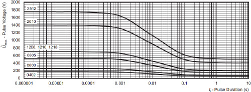
For example, for a 1206 resistor, a maximum voltage of ~500 V can be applied for 10 ms.
3.2.2. Capacitors
In this section, we will discuss ceramic capacitors (types I and II), solid tantalum capacitors and electrolytic capacitors.
3.2.2.1. Ceramic capacitors
The parameter of which the maximum value should not be exceeded is the voltage across the capacitor. This voltage depends on the type of enclosure. Generally, there is no derating mentioned as a function of temperature.
However, certain manufacturers specify (but do not always guarantee) a lifetime under specific conditions (derating), as illustrated below (Murata 2020).

Figure 3.5. Lifetime of an MLCC (multilayer ceramic capacitor) as a function of temperature. For a color version of this figure, see www.iste.co.uk/bayle/maturity1.zip
NOTE.– For this manufacturer, lifetime is defined by the time elapsed until 1% of the components fail;
- – since the three lines are parallel, the activation energy is the same for the three classes of temperature.
3.2.2.2. Tantalum capacitors
For this type of component, there are three parameters for which the maximum value guaranteed by the manufacturer should not be exceeded.
3.2.2.2.1. Direct voltage
Direct voltage is the voltage across the capacitor. It should not exceed the maximum value UR guaranteed by the manufacturer. A temperature derating is provided by the manufacturer (Firadec 2015).

Figure 3.6. Temperature derating of voltage across a tantalum capacitor
This temperature derating curve can be modeled as follows:
with Tmax = 125°C and T85 = 85°C.
3.2.2.2.2. Dissipated power
This is presented in Figure 3.7 (Firadec 2015).
This temperature derating can be modeled as follows:
with a = 1.1279; b = 0.086395; c = 0.018611.

Figure 3.7. Temperature derating of the power dissipated by a tantalum capacitor
3.2.2.3. Electrolytic capacitors
Four stresses should be considered for electrolytic capacitors:
- – The direct voltage applied, equal to the continuous voltage plus the positive peak voltage due to the equivalent series resistance (ESR) of the capacitor.
- – Overvoltage for short periods, which should not exceed 1.15 times the rated voltage guaranteed by the manufacturer.
- – The reverse voltage applied that must be below or equal to 1 V.
- – Storage duration. There is no variation in electrical characteristics when stored for long periods of time, but leakage current may increase. This is due to chemical reactions between the alumina dielectric and the electrolyte. These reactions are reversible when the capacitor is under voltage. The manufacturer normally guarantees storage duration without reformation under well-defined temperature conditions and durations, for example, up to temperatures of 50°C under the following conditions:
- - Voltage below 100 V ➔ 5 years.
- - Between 100 V and 360 V ➔ 3 years.
- - Between 360 V and 500 V ➔ 1 year.
- - Above 500 V ➔ 6 months.

Similar to with tantalum capacitors, it is recommended to have voltage derating depending on the operating temperature. A 60% derating is often recommended.
NOTE.– This type of capacitor is mainly used as an energy reserve (compensating for the power supply microcuts). Due to their large overall external dimensions, a 60% derating rate, as mentioned in the “derating summary” table (Table 3.6), is not achievable at the industrial scale. Moreover, a more significant derating is often considered as going up to 90%.
3.2.3. Magnetic circuits
The parameters to be monitored are:
- – maximum temperature;
- – saturation current.
Generally, there are no derating rules imposed by the manufacturers.
3.2.4. Fuses
The main stresses are:
- – the current through the fuse (breaking capacity);
- – operating temperature;
- – voltage across the fuse when it is “open”.
Generally, there are no derating rules imposed by the manufacturers.
3.2.5. Resonators
The main stress is the operating temperature. Generally, there are no derating rules imposed by the manufacturers.
3.2.6. Oscillators
The main stresses are:
- – operating voltage;
- – supply voltage.
Generally, there are no derating rules imposed by the manufacturers.
3.2.7. Photocouplers
There are many stresses to be considered:
- – photodiode reverse voltage;
- – photodiode reverse peak voltage;
- – photodiode direct current;
- – maximum power dissipated in the photodiode;
- – breakdown voltage VCEo of the phototransistor;
- – breakdown voltage VCBo of the phototransistor;
- – breakdown voltage VBEo of the phototransistor;
- – maximum power dissipated in the phototransistor;
- – maximum operating temperature.
Generally, there are no derating rules imposed by the manufacturers.
3.2.8. Diodes
The main stresses are:
- – maximum direct current If;
- – maximum repetitive peak current IFRm;
- – maximum continuous reverse voltage Vr;
- – maximum repetitive peak reverse voltage VRRm;
- – maximum junction temperature;
- – maximum dissipated power.
Generally, there are no derating rules imposed by the manufacturers.
3.2.9. Zener diodes
The main stresses are:
- – maximum dissipated power;
- – maximum junction temperature.
Generally, there are no derating rules imposed by the manufacturers.
3.2.10. Tranzorb diodes
The main stresses are:
- – maximum pulse power Pppm;
- – maximum operating temperature;
- – steady-state power.
3.2.10.1. Maximum pulse power
Maximum pulse power is derated depending on pulse duration. The curve below, derived from the manufacturer data, is defined for a non-repetitive bi-exponential wave. This is generally how lightning pulses are described in the specifications of the product concerned.

Figure 3.9. Acceptable maximum peak power in a Tranzorb diode
3.2.10.2. Steady-state power
Generally, the manufacturer provides a temperature derating of the steady-state dissipated power, as illustrated below.

Figure 3.10. Temperature derating of the steady-state dissipated power
3.2.10.3. Pulse power
Generally, the manufacturer provides a temperature derating of the steady-state dissipated power, as illustrated below.

Figure 3.11. Temperature derating of the dissipated pulse power
There is no derating for the junction temperature.
3.2.11. Low power bipolar transistors
The main stresses are:
- – collector emitter voltage VCEo;
- – emitter base voltage VBE;
- – collector direct current;
- – junction temperature.
Generally, there are no derating rules imposed by the manufacturers.
3.2.12. Power bipolar transistors
The main stresses are:
- – collector emitter voltage VCEo;
- – emitter base voltage VBE;
- – permanent collector direct current;
- – transient collector direct current;
- – base current;
- – junction temperature.
Generally, there are no derating rules imposed by the manufacturers.
3.2.13. Low power MOSFET transistors
The main stresses are:
- – drain source voltage Vds;
- – grid source voltage Vgs;
- – grid drain voltage Vgd;
- – steady-state direct current ID;
- – pulsed state direct current ID;
- – maximum junction temperature;
- – maximum dissipated power.
Generally, there are no derating rules imposed by the manufacturers.
3.2.14. High power MOSFET transistors
The main stresses are:
- – drain source voltage Vds;
- – grid source voltage Vgs;
- – grid drain voltage Vgd;
- – steady-state direct current ID;
- – pulsed state direct current ID;
- – junction temperature;
- – steady-state dissipated power.
There is generally a derating of the dissipated power depending on the case temperature Tc, as illustrated below.

3.2.15. Integrated circuits
The main stresses are:
- – junction temperature;
- – supply voltage.
Generally, there are no derating rules imposed by the manufacturers.
3.3. Reference-based approach
There are no standards defining the maximum load rate per family of components; however, methodology guides do exist. Load rates often differ from one guide to another, and sometimes the stress parameters of a family of components are not all identical. Moreover, most of the time, these derating rules are not justified and therefore not readily applicable to a given application. Our first approach was to list all the derating values obtained and to thus draw a common basis, as shown by the following table.
Table 3.3. Summary of derating rules according to the literature
| Family of components | Physical contribution | Derating rules |
|---|---|---|
| Resistors | Voltage | 80% |
| Power | 60% | |
| Capacitors | Voltage | 60% |
| Connectors | Current | 60% |
| Fuses | Current | 50% |
| Inductances | Current | 60% |
| Hotspot temperature | 60% | |
| Transformers | Current | 60% |
| Hotspot temperature | 60% | |
| Voltage | 60% | |
| Diodes | Reverse voltage | 75% |
| Junction temperature | 70% | |
| Optocouplers | Voltage | 75% |
| Reverse voltage | 75% | |
| Junction temperature | 70% | |
| Bipolar transistors | Voltage Vce | 75% |
| Voltage Vbe | 75% | |
| Junction temperature | 70% | |
| MOSFET transistors | Voltage Vds | 75% |
| Voltage Vgs | 75% | |
| Junction temperature | 70% | |
| Analog circuits | Supply voltage | 75% |
| Junction temperature | 80% | |
| Logic circuits | Supply voltage | 75% |
| Junction temperature | 80% |
NOTE.– The rates in the table are an average of the rates issued from the following guides:
- – MIL-HDBK-338B (1988);
- – NAV-SEA (1991);
- – MIL-STD-975 NASA (2003).
3.4. Creation of derating rules
The derating rules proposed in this book were established in order to provide a justification for the rules generally used in the design of electronic circuits. This analysis relies on the physics of the failure of components.
It therefore seems appropriate to take into account the reliability level of the component, depending on the physical contribution involved in these derating rules. More specifically, the focus will be on the sensitivity of component reliability with respect to the empirical acceleration law modeling the influence of the considered physical contribution.
As already noted, the derating rate is defined as the ratio of the value applied to the component and the maximum value guaranteed by the manufacturer of the component. It therefore ranges between 0 and 100%. It therefore seems relevant to consider that the maximum acceptable derating DR_Max is applicable to the family of components most sensitive to the physical contribution being considered.
Moreover, it is appropriate to take a minimal derating rate DR_Min to avoid needless overdesign. This derating rate will be assigned to the family of components least sensitive to the applied physical contribution. The value of this margin depends on the type of application (consumer products, aeronautics, automotive and aerospace industries, etc.).

Figure 3.13. Compromise between reliability and overdesign. For a color version of this figure, see www.iste.co.uk/bayle/maturity1.zip
The value of these derating rates is the result of a compromise between “overdesign” and a good level of reliability, as illustrated in the figure above.
This qualitative analysis must be followed by a quantitative approach to building these rules. This involves using the sensitivity of a function of a given parameter as the ratio between the relative variation of the function and the relative variation of the considered variable. The sensitivity of the function “f” with respect to the variable x is given by:
An equivalent form of the sensitivity of a function is generally expressed as:
For the derating, the function “f” is considered as the acceleration factor of the underlying physical law governing the failure. As for the parameter “xp”, the characteristic parameter of this law is considered (e.g. the activation energy for the temperature). The following derating rule “DR” is then proposed:
where “a” and “b” are two parameters to be calculated. The problem is that the parameter “p” can take various values depending on the type of component and therefore on the failure mechanism being considered. Therefore, two extreme cases must be considered, namely the minimum value p_min and the maximum value p_max. The previous qualitative rules lead to the following product of equations:
The values of DR_Max and DR_Min correspond, respectively, to the minimal and maximum values of the derating rules. The method proposed here is first illustrated in Figure 3.14.
A compromise between the robustness margin and overdesign can lead to the following rules:
- – DR_Max = 90%;
- – DR_Min = 50%.

Figure 3.14. Illustration of derating rules. For a color version of this figure, see www.iste.co.uk/bayle/maturity1.zip
The next step is then to determine the values of the parameters DR_Max and DR_Min. These values depend on the field of application and should therefore be estimated by those responsible for derating studies in the company concerned. For example, the MIL-HDBK-338B handbook (MIL 1998) provides similar information in the following table.
| PART TYPE | DERATING PARAMETER | DERATING LEVEL | ||
| I (Space) | II (Airborne) | III (Ground) | ||
|
TRANSISTORS
| On-State Current (It – % Rated) | 50% | 70% | 70% |
| Off-State Voltage (VDM – % Rated) | 70% | 70% | 70% | |
| Max T (°C) | 95° | 105° | 125° | |
| Power Dissipation (% Rated) | 50% | 60% | 70% |
| reakdown Voltage (% Rated) | 60% | 70% | 70% | |
| Max T (°C) | 95° | 105º | 125° | |
| Power Dissipation (% Rated) | 50% | 60% | 70% |
| Breakdown Voltage (% Rated) | 60% | 70% | 70% | |
| Max T (°C) | 95° | 105° | 125° | |
For certain applications, such as those in the aerospace sector, where the stakes of reliability, safety, etc. are very high, the following rules can be considered:
- – DR_Max = 80%;
- – DR_Min = 30%.
The next step is to calculate parameters a and b satisfying the previous product of equations, depending on the physical law of the failure. The result is then:

PROOF.–
The previous product of equations leads to:

The ratio of the two equations term by term leads to eliminating parameter a. Parameter b can then be calculated as follows:
The natural logarithm of the previous equation gives:
or finally

Inserting the value of b in the first equation, the value of parameter “a” is obtained.
or finally
End
The derating rules are then written for constant temperature as follows:
PROOF.–
As already noted: ![]() therefore:
therefore: ![]()
Hence:
End
3.4.1. Rules for constant temperature
The failure mechanisms accelerated by temperature are generally governed by the Arrhenius law (Arrhenius 1889) whose acceleration factor is given by:
NOTE.– This is an acceleration with respect to the reference temperature θo.
- – Here, T designates the junction temperature θj for the active components and the hotspot temperature Th for the passive components.
Let us then study the sensitivity of this acceleration factor with respect to the activation energy Ea. This can be written as:
or
Consequently, parameters “a” and “b” are written as:

The derating rules can then be written for the constant temperature as:
PROOF.–
It is known that: ![]() and that
and that ![]()
Combining these two equations leads to:

or finally:

End
Based on the FIDES guide for predictive reliability (FIDES 2009), the following table presents activation energy as a function of component type.
Table 3.4. Activation energy for various types of components
| Types of components | Ea (eV) |
|---|---|
| Ceramic capacitors | 0.1 |
| Electrolytic capacitors | 0.4 |
| Tantalum capacitors | 0.15 |
| Plastic capacitors | 0.25 |
| CMS resistors | 0.15 |
| Fuses | 0.15 |
| Magnetic components | 0.15 |
| Diodes | 0.7 |
| Transistors | 0.7 |
| Integrated circuits | 0.7 |
| LED | 0.6 |
| Optocouplers | 0.4 |
| ASIC | 0.7 |
| Relay | 0.25 |
| Interrupters and switches | 0.25 |
| Connectors | 0.1 |
| Hybrid | 0.7 |
| RF and HF Circuits | 1.5 |
| LCL STN screen | 0.6 |
| LCD TFT screen | 0.5 |
| Lithium battery | 0.4 |
Therefore, Ea_Min = 0.1 eV and Ea_Max = 0.7eV. Using the proposed derating rules, the following derating rates are obtained.
| Types of components | Derating |
|---|---|
| Ceramic capacitors | 50% |
| Connectors | 50% |
| Tantalum capacitors | 54.6% |
| CMS resistors | 54.6% |
| Fuses | 54.6% |
| Magnetic components | 54.6% |
| Plastic capacitors | 61% |
| Relay | 61% |
| Interrupters and switches | 61% |
| Electrolytic capacitors | 67.6% |
| Optocouplers | 67.6% |
| Lithium battery | 67.6% |
| LCD TFT screen | 70.9% |
| LED | 73.8% |
| LCL STN screen | 73.8% |
| Diodes | 76.3% |
| Transistors | 76.3% |
| Integrated circuits | 76.3% |
| ASIC | 76.3% |
| Hybrid | 76.3% |
| RF and HF circuits | 90.0% |
This can be illustrated by Figure 3.15.
To illustrate the method, the acceleration factor can be calculated with respect to a maximum temperature of 125°C, and to the derated temperature, as illustrated in Figure 3.16.

Figure 3.15. Derating rate depending on activation energy. For a color version of this figure, see www.iste.co.uk/bayle/maturity1.zip

Figure 3.16. Acceleration factor depending on the derated temperature. For a color version of this figure, see www.iste.co.uk/bayle/maturity1.zip
It can be noted that the acceleration factors are relatively homogeneous.
3.4.2. Rule for voltage
Failure mechanisms accelerated by voltage are generally governed by a power law whose acceleration factor is given by:
Let us study the sensitivity of this acceleration factor with respect to parameter ∈. The following relation can be written:
or

This leads to:
PROOF.–
It is known that: ![]() and that
and that ![]()
Combining these two equations leads to:

or

End
3.5. Summary
The proposed method for the estimation of derating rules relies on the physical laws of failure. Unfortunately, the parameters of a component that are guaranteed by the manufacturer cannot all be modeled by the laws of physics. Therefore, in order to have a summary of the various rules proposed (by the manufacturer, by standards and by the proposed method), only the parameters meeting this constraint are listed in the following table.
Table 3.6. Summary of derating rules
| Family of components | Physical contribution | Derating references | Proposed derating |
|---|---|---|---|
| Chip resistors | Hotspot temperature | 80% | 54.6% |
| Ceramic capacitors | Hotspot temperature | 60% | 50% |
| Direct voltage | 60% | 71.7% | |
| Electrolytic capacitors | Hotspot temperature | 60% | 67.6% |
| Direct voltage | 90% | 71.7% | |
| Tantalum capacitors | Hotspot temperature | 60% | 54.6% |
| Direct voltage | 60% | 71.7% | |
| Transformers | Hotspot temperature | 60% | 54.6% |
| Inductances | Hotspot temperature | 60% | 54.6% |
| Connectors | Hotspot temperature | Tmax – 25% | 50% |
| Fuses | Hotspot temperature | 50% | 54.6% |
| Diodes | Junction temperature | 70% | 76.3% |
| Optocouplers | Junction temperature | 70% | 67.6% |
| Bipolar transistors | Junction temperature | 70% | 76.3% |
| Analog circuits | Junction temperature | 80% | 76.3% |
| Logic circuits | Junction temperature | 80% | 76.3% |
| RF and HF circuits | Junction temperature | 80% | 90% |