3
Design and Optimization for Reliability
3.1 Introduction
Design for reliability (DFR) encompasses a set of tools that support product and process management from concept development, prototyping, new product introduction, volume production, and all the way through retirement. With affordable repair and maintenance costs, the goal of DFR is to ensure that customer expectations for reliability are fully met across a product lifecycle. In this chapter, we introduce several DFR tools that are commonly used by reliability practitioners and design engineers: reliability and redundancy allocation (RRA), failure‐in‐time (FIT) design, design for six‐sigma (DFSS), fault‐tree analysis (FTA), and failure mode, effect, and criticality analysis (FMECA). While RRA is implemented at the component level, both FIT and DFSS are often used in the detailed design of subsystems or assemblies. FTA uses a top‐down approach to investigate the root cause of systems failure and to determine the ways to reduce the risk of such failures. FMECA allows the design engineers to identify and rank the potential failure modes in the early development phase, and further determine the remedies to remove or mitigate the risk of failures.
3.2 Lifecycle Reliability Optimization
3.2.1 Reliability–Design Cost
Reliability can be designed in during the product development and prototyping stage. It is generally agreed that the design and development costs increase exponentially with the reliability of the item, including hardware and software (Huang et al. 2007; Guan et al. 2010). This is mainly due to the fact that when reliability reaches a certain level, the efforts and the resources required for further reduction of the failure rate increases much faster than the reliability gain. Let cd(r) be the product design and development cost with reliability r for 0 < r ≤ 1. Mettas (2000) proposes the following exponential model to characterize the relation between the reliability and the cost:

The model contains four non‐negative parameters, namely, rmin, rmax, k, and c0. Note that rmin represents the minimum acceptable reliability required by the customers; rmax is the maximum reliability that can be achieved by the manufacturer. Obviously the condition 0 < rmin < rmax ≤ 1 always holds and k for 0 ≤ k ≤ 1 is the feasibility of increasing the reliability. A large k implies that it is relatively easy, and hence less costly, to increase the reliability based on current manufacturing technology and available materials. Finally c0 is the baseline design and development cost with r = rmin.
Figure 3.1 shows how cd(r) increases with the reliability r for different values of rmin. These curves are generated assuming rmax = 1, k = 0.3, and c0 = 1. It is also found that to achieve the same reliability level, it is more costly to improve the product with lower reliability. This observation make senses because a product with a low reliability requires more resources and effort to bring it to a high level compared with a reliable product.

Figure 3.1Reliability–design cost under different rmin with rmax = 1, k = 0.3 and c0 = 1.
Depending on the nature of the product and existing technologies, reliability of certain components can be more difficult to improve compared with others. For example, in an airplane, it is relatively easy to improve the reliability of the avionics than the engine because the operation condition and the structure of the latter is much more complicated than the former. Parameter k represents the degree of difficulty to increase a product's reliability. Given rmin = 0.7, rmax = 1, and c0 = 1, Figure 3.2 depicts how the reliability design cost increases with r corresponding to k = 0.1, 0.5, and 0.8, respectively. It shows that for a larger k, less cost is required in order to achieve the same reliability level.
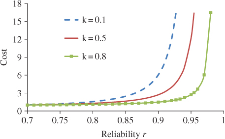
Figure 3.2Reliability–design cost under various k with rmin = 0.7, rmax = 1 and c0 = 1.
Sometimes the failure rate, instead of the reliability, is more convenient to capture the relation between reliability and design cost. For instance, the failure rate is often used to measure the reliability of a software product or program. Instead of the total cost, the incremental design cost sometimes is more interesting to the manufacturer as it measures the reliability growth as a result of additional investment. Let b(α) be the incremental reliability–design cost for a product. Then a variant of Eq. 3.2.1 is given below
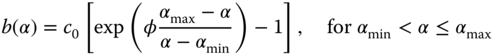
where αmax and αmin are the maximum acceptable and the minimum achievable failure rate, respectively. Note that c0 is the baseline design cost when α = αmax and φ is a positive parameter characterizing the difficulties in reliability growth. In general, a large φ implies that more effort and resources are required in order to achieve the same reliability performance.
3.2.2 Reliability–Manufacturing Cost
During the manufacturing stage, product reliability can be improved if one adopts new materials, advanced quality control, and the latest manufacturing technology. Jiang and Murthy (2009) have discussed how the quality variations affect the product reliability. In general, the manufacturing cost increases with the product reliability. Though the actual relation between reliability and manufacturing cost is often product‐dependent, Öner et al. (2010) propose a reliability–manufacturing cost model by assuming a nonlinear relation between the failure rate and the cost as follows:
The model has three parameters, p0, p1, and ν, where p0 is the baseline unit manufacturing cost at the maximum failure rate, and p1 and ν capture the incremental cost as the failure rate α is reduced with respect to αmax. Particularly, ν captures the degree of difficulties in reducing the failure rate given the current manufacturing technology or raw materials. This model assumes that the design phase is relatively short compared to the product useful lifetime. Hence, the impact of the learning effect is not considered. Reliability–manufacturing cost models incorporating the learning effects are available in Teng and Thompson (1996).
Figure 3.3 depicts the unit manufacturing cost versus the failure rate under ν = 0.3, 0.5, and 0.7, respectively. Curves A, B, and C are plotted with the same values of p0 = $400, p1 = $50, and αmax = 0.01. For large ν, it is more costly to improve the product reliability through the manufacturing process. C and D are plotted with the same value of ν, but different p1. A larger p1 implies that more resources are required in order to maintain the same failure rate. Therefore, a trade‐off must be made between the DFR and the design for manufacturing so as to achieve the reliability target at a minimum cost. This will be discussed in the next section.

Figure 3.3Reliability–manufacturing cost with αmin = 0.005 and αmax = 0.01.
3.2.3 Minimizing Product Lifecycle Cost
A main objective in reliability optimization is to optimize the resource allocation across product design, manufacturing, and field support such that the lifecycle cost is minimized. In this section, we present a DFR optimization model to facilitate the product manufacturer to achieve this objective. In our setting, we assume that the manufacturer offers free repair and replacements during the warranty period. The goal is to optimize the product reliability such that the costs associated with design, manufacturing, and warranty services are minimized. The following notation used in the model is defined:
- T = length of the warranty period (year)
- p2 = annual repair or replacement cost per unit product ($/unit/year)
- Q = number of products shipped to the customers
The optimization model is formulated to minimize the total costs of all installed products during the warranty period T. These costs include design, manufacturing, and warranty services.
Figure 3.4 graphically shows the relations between design cost, manufacturing cost, and warrant repair cost. On one hand, to decrease the failure rate, more investments are required in product design and manufacturing stages, but the warranty cost will be saved because of reduced failure returns. On the other hand, we can save the design and manufacturing costs by accepting a relatively high product failure rate, but the warranty cost will escalate because of high field returns. Therefore, the manufacturer needs to determine the optimal α* that can balance the trade‐off between design, manufacturing, and warranty costs. We take the derivative with respect to α in Eq. 3.2.4 and set it to zero. It yields
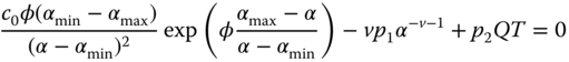
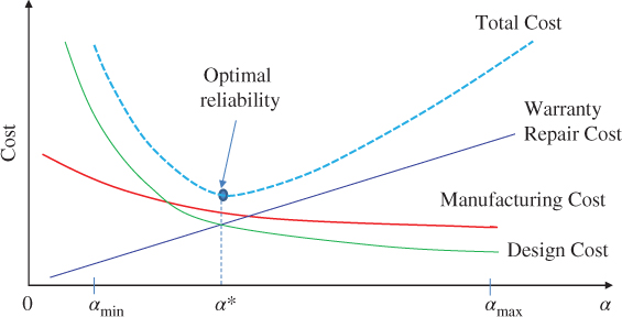
Figure 3.4Sum of the design, manufacturing, and warranty costs.
The optimality is guaranteed because C(α) is the convex function between [αmin, αmax]. Namely,
Hence, the optimal value of α* is the one that satisfies Eq. 3.2.6. Unfortunately, there is no closed‐form solution to α*. Thus one can find α* by using the iteration search over the interval between [αmin, αmax]. Below we present a numerical example to illustrate this method.
3.3 Reliability and Redundancy Allocation
The RRA model is a mathematical programing that guides the design engineer to achieve the following objectives: (i) minimize the product resources while attaining the reliability goal or (ii) maximize the system reliability without violating the resource constraints. We discuss the cost minimization problem in this section.
For reliability allocation models, the component reliability is treated as a decision variable. For redundancy allocation models, the decision variable is the level of redundancy and the choice of component types. Most papers focus on a single objective, while some have addressed multiobjective optimization. Various mathematical programming techniques have been used to solve reliability–redundancy optimization problems. These techniques include dynamic programming (Fyffe et al. 1968), integer programming, mixed integer programming (Ghare and Taylor 1969; Bulfin and Liu 1985), heuristics, genetic algorithms (Coit and Smith 1998; Taboada et al. 2008), and a solution space reduction procedure combined with branch‐and‐bound (Sung and Cho 1999), among others. Each technique is effective in solving some particular optimization problems. Readers are referred to the book by Kuo and Zuo (2003) for a comprehensive treatment on this topic. In this section, typical RRA models are reviewed in terms of problem formulation and basic solution techniques.
3.3.1 Reliability Allocation for Cost Minimization
For multicomponent system design, it is often useful to predict the reliability of the system based on individual component reliability. The question is how to meet the reliability target of the system subject to cost and operational constraints? The simplest answer to this question is to distribute the reliability goal equally among all subsystems or components. However, such allocation may not be feasible or optimal in terms of minimizing the cost, weight, and volume of a product.
Take the three‐component system in Figure 3.6 as an example. If the target system reliability is Rs = 0.95, then we have various options to achieve the goal. For instance, we may choose r1 = 0.979 and r2 = r3 = 0.83, which leads to Rs = 0.951; or we can also assign r1 = 0.96, r2 = 0.98, and r3 = 0.52, which yields Rs = 0.951. Both designs meet the system reliability target. In Design 1, components 2 and 3 have medium reliability, while in Design 2, reliability of component 2 is high, but it is low for component 3. Obviously, the total system cost is likely to be different because component costs are correlated with reliability. Reliability allocation is a method of apportioning a system's target reliability among different components. Hence, it is a useful tool for design engineers to determine the required reliability of individual components to achieve the system reliability goal with minimum cost, time, and other resource consumptions. Such requirement can be met by solving the following reliability optimization problem, denoted as Model 3.2.
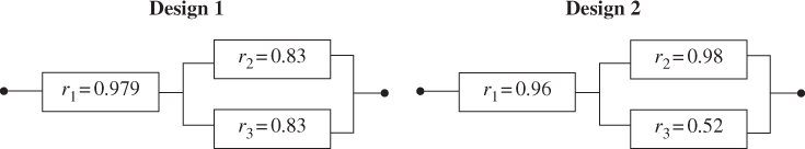
Figure 3.6Two design options for a series–parallel system.
3.3.2 Reliability Allocation under Cost Constraint
Sometimes the design budget like cost is limited; then the objective becomes how to allocate the budget to individual components such that the overall system reliability is maximized. Hwang et al. (1979) proposes a reliability allocation model to maximize the reliability of complex systems subject to resources constraints. The problem is formulated as follows.
3.3.3 Redundancy Allocation for Series System
A redundancy allocation problem (RAP) deals with how to build a parallel structure to effectively increase the system reliability. Hence the decision variable is the level of redundant units for a component type. This differs from the reliability allocation problem in which the component's reliability is the design variable. If multiple component types are available to a subsystem, the choice of component types is also a decision variable. For series–parallel systems, if subsystems allow multiple component type choices, Chern (1992) has proved that the redundancy allocation problem is indeed NP‐hard. Dynamic programming, mixed integer programing, and heuristic algorithms have been used to solve this type of problem. Liang and Smith (2004) developed an ant colony meta‐heuristic method to solve the RAP where different components can be placed in parallel. The general formulation for RAP for a series system under cost constraint is defined as follows.
3.3.4 Redundancy Allocation for k‐out‐of‐n Subsystems
For a series system comprised of multiple k‐out‐of‐n subsystems, redundancy allocation aims to meet the reliability of the whole system while minimizing the total cost. Take the automated test equipment (ATE) as an example. ATE is a capital‐intensive machine widely used for wafer probing and testing in the back end of semiconductor manufacturing. The downtime cost of ATE is expensive and typically in a range between $10 000 and $50 000/hour depending on the device under test. Hence k‐out‐of‐n:G redundant configuration is often adopted to ensure the reliability of the ATE system. Figure 3.9 shows the reliability block diagram of an ATE system comprised of four subsystems in series: high‐speed digital (HSD), analog, direct current (DC), and microwave (MW).
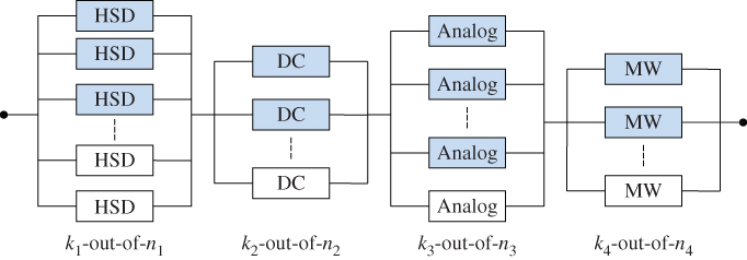
Figure 3.9k‐out‐of‐n subsystem redundancy allocation in ATE.
To test a device, a minimum number of modules (components) must be available for each subsystem. For instance, for the analog subsystem, at least k3 modules should be good in order to generate a sufficient number of analog waveforms feeding into the device under test. The redundant modules in each subsystem usually act as a hot‐standby mode, and can immediately resume the testing load if any active modules fail. Hence the reliability of a subsystem can be modeled as a ki‐out‐of‐ni:G system, where ki are the minimum required working units and ni are the maximum components for subsystem i. The goal is to determine the redundant units for each subsystem, denoted as xi = ni − ki, such that the ATE meets the target reliability while the cost is minimized.
Model 3.5 is a MINL problem. In general, this type of problem is difficult to solve because of its combinatorial nature coupled with the non‐linearity. Below we propose a heuristic method to tackle this optimization problem. The procedure consists of six steps.
Heuristic Algorithm for Redundancy Allocation of k‐out‐of‐n Subsystems:
- Step 1: Calculate the minimum reliability required for each subsystem, i.e.
 .
. - Step 2: Compute the reliability of all subsystems for given ki at xi = 0 for i = 1, 2, …, s.
- Step 3: If Ri ≥
 for all i, there is no need of redundancy allocation, so go to Step 5. Else go to the next step.
 - Step 4: Increase xj = xj + 1 and compute the reliability Rj. If Rj >
 , then go to Step 5. Else let xj = xj + 1 and compute Rj, until Rk ≥
  .
. - Step 5: Given all the feasible solution set of x = {x1, x2, …, xs}, estimate the total cost using Eq. 3.3.15.
- Step 6: Choose the x with the lowest cost g(x) as the optimal solution.
Below we present a numerical example to illustrate the application of the heuristic optimization algorithm.
3.4 Multiobjective Reliability–Redundancy Allocation
3.4.1 Pareto Optimality
Quite often maximizing the system reliability or minimizing the cost is not sufficient as reliability estimates or system operation conditions often involve uncertainty. Therefore it is desirable to incorporate the reliability estimation uncertainties into the optimization model in order to achieve robust system design. For risk‐averse system operation, it is desirable to maximize the system reliability as well as to minimize its uncertainty. This type of design requirement can be realized under a multiobjective optimization framework, where the decision‐makers can choose the best comprised design from a set of non‐dominant solutions. A typical multiobjective optimization problem (MOOP) can be formulated as follows.
3.4.2 Maximizing Reliability and Minimizing Variance
In Chapter 02, we discussed how to estimate the system reliability based on the component reliability estimate. Since reliability estimates always involve estimation uncertainties, it is desirable to reduce the variability of the system reliability when performing reliability–redundancy allocations. Assuming that component reliability estimates are statistically independent, we present a MOOP model to maximize the reliability of a series system and to minimize its variance.
3.4.3 Numerical Experiment
We use the numerical example in Coit et al. (2004) to demonstrate the application of Model 3.8. The system has three subsystems in series and five component choices (or types) in each subsystem. Table 3.5 lists all component data including mean reliability rij, variance of the reliability estimate (![]() ), unit cost and weight. Design constraints on the system level are maximum cost C = 29 and a maximum weight W = 45. For this problem, all component reliability estimates are statistically independent.
), unit cost and weight. Design constraints on the system level are maximum cost C = 29 and a maximum weight W = 45. For this problem, all component reliability estimates are statistically independent.
Table 3.5 Component reliability, cost, and weight.
Source: Reproduced with permission of IEEE.
| Subsystem 1 (i = 1) | Subsystem 2 (i = 2) | Subsystem 3 (i = 3) | ||||||||||||
| j | rij | cij | wij | j | rij | cij | wij | j | rij | cij | wij | |||
| 1 | 0.96 | 0.0043 | 8 | 5 | 1 | 0.98 | 0.0020 | 6 | 5 | 1 | 0.95 | 0.0059 | 7 | 6 |
| 2 | 0.92 | 0.0067 | 6 | 6 | 2 | 0.93 | 0.0109 | 3 | 7 | 2 | 0.89 | 0.0196 | 5 | 8 |
| 3 | 0.86 | 0.0120 | 6 | 8 | 3 | 0.88 | 0.0088 | 4 | 3 | 3 | 0.87 | 0.0071 | 4 | 5 |
| 4 | 0.77 | 0.0253 | 3 | 6 | 4 | 0.69 | 0.0238 | 3 | 5 | 4 | 0.71 | 0.0257 | 3 | 5 |
| 5 | 0.68 | 0.0181 | 3 | 5 | 5 | 0.6 | 0.0120 | 4 | 3 | 5 | 0.65 | 0.0190 | 2 | 4 |
When solving Model 3.8 by the weighted objective method as described in Section 3.4.1, there are two weights, v1 and v2, in the objective function shown in Eq. 3.4.10 below. The values of the weights are alternated in order to obtain different non‐dominant solutions of the original problem. The problem is solved repeatedly by varying the value of v1 from 1 to 0 (or v2 = 1 − v1) using the GA algorithm. The importance of original objective functions is controlled by the relative size of two weights:
Three non‐dominant solutions listed in Table 3.6 constitute the Pareto optimal solutions. For instance, if solution A is chosen, the reliability ![]() = 0.9844 would be the highest, but
= 0.9844 would be the highest, but ![]() = 0.000 438 is also the largest. If solution C is chosen,
= 0.000 438 is also the largest. If solution C is chosen, ![]() would be the lowest, but
would be the lowest, but ![]() is also the smallest. Therefore, A, B, and C form a set of non‐dominant designs.
is also the smallest. Therefore, A, B, and C form a set of non‐dominant designs.
Table 3.6 Pareto optimal solutions for independent component estimates.
Source: Reproduced with permission of IEEE.
| Solution | Subsystem 1 | Subsystem 2 | Subsystem 3 | ||||||||||||||
| x11 | x12 | x13 | x14 | x15 | x21 | x22 | x23 | x24 | x25 | x31 | x32 | x33 | x34 | x35 | |||
| A | 0 | 1 | 0 | 2 | 0 | 0 | 2 | 0 | 0 | 0 | 1 | 0 | 1 | 0 | 0 | 0.9844 | 4.38 × 10⁻⁴ |
| B | 0 | 2 | 0 | 0 | 0 | 0 | 2 | 0 | 0 | 0 | 0 | 0 | 1 | 1 | 2 | 0.9842 | 3.80 × 10⁻⁴ |
| C | 0 | 1 | 0 | 1 | 1 | 0 | 2 | 0 | 0 | 0 | 0 | 0 | 2 | 0 | 1 | 0.9834 | 3.53 × 10⁻⁴ |
These three non‐dominant solutions are mapped into the corresponding system configurations (see Figures 3.13–3.15). An important observation is that as v1 decreases, it becomes more important to minimize the variance of the reliability estimate and less important to maximize the system reliability. Hence the design changes accordingly.

Figure 3.13Pareto optimal solution  = 0.9844,
  = 0.000438.
Figure 3.14Pareto optimal solution  = 0.9842,
  = 0.00038.
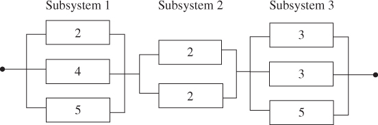
Figure 3.15 Pareto optimal solution  = 0.9834,
  = 0.000353.
The topic of RRA has continued to receive attention recently. There are three new research trends that have been observed. First, the traditional RRA problem is expanded to incorporate other reliability programs, such as the reliability growth test (Heydari and Sullivan 2018), during the product development stage. Second, efforts are also made to jointly allocate reliability–redundancy and maintenance policy (Bei et al. 2017) and joint allocation of reliability–redundancy and spare parts inventory (Jin et al. 2017). The third direction is to extend RRA to a more complex system structure with independent failure, such as network systems and failure corrections (Yeh and Fiondella 2017).
3.5 Failure‐in‐Time Based Design
3.5.1 Component Failure Rate Estimate
In the early design phase, a reliability prediction is often required for the components and systems in order to assess their future reliability and in many cases to meet customer specifications. For instance, IEEE issued a standard methodology (i.e. IEEE 1413) for the reliability prediction of electronic systems (IEEE 1413 1998; Pecht et al. 2002). The prediction model is built on the assumption of the exponential lifetime of components with independent failures. It is understood that the accuracy of the reliability prediction depends on two factors: (i) the appropriateness of the model to the component lifetime distributions and (ii) the completeness of the component information, such as derating, temperature, and other environmental stresses. Table 3.7 summarizes the empirical and standard‐based prediction methods adopted in the US, China, France, Japan, and Germany.
Table 3.7 Empirical and standard based prediction methods (ReliaSoft 2017).
| Nation | Prediction method | Applications | Last updated |
| USA | MIL‐HDBK‐2017F and Notice 1 and 2 | Military/Defense | 1995 |
| USA | Bellcore/Telcordia | Telecom | 2006 |
| France | RDF 2000 | Telecom | 2000 |
| SAE USA | SAE Reliability Prediction | Automotive | 2017 |
| Japan | NTT Procedure | Telecom | 1985 |
| Germany | Siemens SN29500 | Siemens Products | 1999 |
| China | China 299B | Military/Defense | 1998 |
| USA | PRISM | Military/Commercial | 2000 |
| USA | IEEE 1413 | Electronics | 2002 |
Though various reliability prediction methods have been developed, the two standards mostly used by industry to forecast the new product reliability are MIL‐HDBK‐217F (US MIL‐HDBK217 1995) and Bellcore TR332 (Bellcore 1995). Both standards predict the reliability of a new product by combining component failure rates and the bill of materials (BOMs). The Bellcore/Telcordia predictive method for an individual component is of the form
where
| λb | = | the base failure rate or the nominal failure rate |
| πQ | = | the quality factor |
| πT | = | the temperature stress factor |
| πE | = | the electrical stress factor |
| πO | = | other factors such as humidity, usage, and vibrations |
In the electronics industry, the nominal failure rate λb is usually estimated at 40 °C operating temperature with 50% of the electrical derating rate. Derating puts the operation of a device at lower than its rated maximum capability in order to extend its life. Typical electrical derating includes the voltage, current, and power. FIT is an alternative way to measure the product lifetime. It reports the number of failures per 109 hours (or 1 billion hours) of operation of a unit. For instance, a component with 100 FIT is equivalent to 109/100 = 107 hours mean‐time‐between‐failures (MTBF) for repairable system or mean-time-to-failure (MTTF) for non-repairable system. Therefore λo and λb in Eq. 3.5.1 can be expressed as either FIT or failures per unit time, depending on the application and industry preference.
3.5.2 Component with Life Data
A new design is often built upon the success or experience of legacy products with similar functions or operating conditions. Many technologies and components used in predecessor products are most likely to be reused in the new product. Therefore, reliability or failure rate of these components can be appropriately estimated from field failures of legacy products. This can be achieved through the following model:

where ![]() is the estimate of the component's true failure rate λ. This result from this model is rather accurate as long as the operating condition and electrical derating of the component in the new product are similar to the predecessors. We use the following numerical example to illustrate the estimation process.
is the estimate of the component's true failure rate λ. This result from this model is rather accurate as long as the operating condition and electrical derating of the component in the new product are similar to the predecessors. We use the following numerical example to illustrate the estimation process.
3.5.3 Components without Life Data
For components without sufficient field data, their failure rate can be appropriately extrapolated based on the operating temperature and the derating rate. Component suppliers usually provide the base failure rate λb that represents the nominal reliability performance when they operate under the nominal conditions (e.g. 40 °C at 50% derating level for electronics). According to Eq. 3.5.1, the actual failure rate depends on πQ, πT, and πE factors. Since πQ is largely determined by the commodity supplier and πQ is associated with the usage, the most effective way that a design engineer wants to prolong the component lifetime is to reduce the temperature stress, the derating rate, or both. Let us assume that πQ = πR = 1. Then Eq. 3.5.1 becomes
The temperature factor πT can be estimated using the Arrhenius model, which is given by (Elsayed 2012)
where
| Ea | = | activation energy (eV) |
| k | = | Boltzman constant (8.62 × 10⁻⁵eV/K) |
| T0 | = | reference ambient temperature (313 K) |
| T | = | component ambient temperature (K) |
In Figure 3.16 we plot the value of πT as T increases from −40 °C to 80 °C for Ea = 0.2, 0.4, and 0.6 eV, respectively. Two important observations are obtained. First, πT is relatively insensitive to the activation energy Ea if T < 40 °C. However, when T exceeds 40 °C, components with higher Ea fail much faster than those with lower Ea. Second, lowering the ambient temperature is critical to extending the component lifetime, especially for large Ea. For instance, a component with Ea = 0.6 eV, its πT doubles whenever T increases by 10 °C, or equivalently cutting its lifetime by 50%.

Figure 3.16Ambient temperature versus the temperature factor.
According to Bellcore 332 (Bellcore 332 1995/Telcordia TR‐332), the electrical derating factor πE can be estimated by the following equation as
where
| p | = | actual electrical derating percentage |
| p0 | = | reference derating with p0 = 50% |
| m | = | fitting parameter |
The fitting value m ranges from 0.006 to 0.059 depending on the nature of the component and its composition materials. For details of values of m, one can refer to Telcordia TR‐332 (Telcordia TR‐332). Here we partially list the value of “m” for certain electronic devices, where m is in the range of [0.019, 0.024] (see Table 3.9). The following example illustrates the use of Eq. 3.5.6.
Table 3.9 Parametric value of m for certain electronic devices.
| Component | 1 MB EPROM | 0.2 W 1% resistor | FPGA | Switch transistor | Optional amp | Clock driver |
| m | 0.024 | 0.019 | 0.024 | 0.024 | 0.024 | 0.024 |
3.5.4 Non‐component Failure Rate
Besides the component (i.e. hardware) failures, there are many system‐level failures caused by non‐component issues. Typical non‐component failures include design issues, manufacturing defects, software bugs, incorrect process, and no‐fault‐found (NFF). NFF happens when a part or field replacement unit is returned to the repair center for trouble shooting, but diagnostic tests are not able to duplicate the failure mode that occurred at the customer's site. More discussions about NFF will be provided in Chapter 04.
Non‐component failure rates are usually more difficult to estimate than component failure rates. This is because non‐component failure rates are influenced by a variety of factors, and some of them are human‐related. For example, design errors and software bugs are correlated with the engineers' experience and the similarity to the predecessor product. Poor solder joints are closely associated with the complexity of the product and the reflow temperature. Process issues can be avoided by providing good training to employees or product users. Similar to the component failure rate, the non‐component failure rate, denoted as λ, can be estimated as

where ![]() represents the estimate of λ. Failures of non‐component related issues include design errors, manufacturing defects, software bugs, process issues, and NFF. We use the following example to illustrate the application of Eq. 3.5.7.
represents the estimate of λ. Failures of non‐component related issues include design errors, manufacturing defects, software bugs, process issues, and NFF. We use the following example to illustrate the application of Eq. 3.5.7.
3.6 Failure Rate Considering Uncertainty
3.6.1 Temperature Variation
It is quite common that multiple units of the same component type are used in a system. If the variation of the ambient temperature across these units is small, a single temperature reading T or the average temperature is adequate to calculate the temperature factor πT in Eq. 3.5.5. When a large variation of temperature is observed, a single‐point value of temperature becomes inadequate to estimate πT. Figure 3.18 shows the temperature readings of 32 integrated devices called application‐specific integrated circuits (ASICs) on a printed circuit board (PCB) module. The temperature varies from 65 °C to 88.2 °C with a maximum range of 23.2 °C when it is used in the field. This implies that the devices under 88.2 °C will fail more than twice as fast as those under 65 °C. The temperature variation in this case fits the normal distribution with mean 76.3 °C and the standard deviation 5.7 °C.
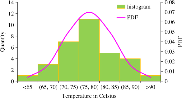
Figure 3.18Temperature distribution of ASIC units in a PCB module.
To characterize the failure rate uncertainty that resulted from temperature variations, πT should be treated as a random value. Based on the temperature distribution profile, the mean and the variance of πT can be estimated as follows (Jin and Su 2005):
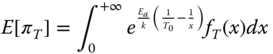

where fT(x) is the probability density function (PDF) of T. Modern electronic devices such as microprocessors, FPGA, and ASIC usually have built‐in temperature sensors, and the real‐time temperature can be directly measured, transferred and stored in a computer server for further analysis. To protect the outlier data, repeated sampling and multiple temperature readings are recommended for each component.
3.6.2 Electrical Derating Variation
For the same component type in a PCB module, electrical derating such as power, voltage, or current may vary from one unit to other depending on the circuitry architecture and the functional requirements. Figure 3.19 shows the voltage derating percentage of 82 identical 10‐V capacitors within a PCB module. The derated percentage varies from 50% to 85% with a maximum difference of 35%. Note that 50% derating equals 5 V and 85% derating corresponds to 8.5 V. The information about electrical derating can be obtained from the product design engineers who are responsible for determining the components and laying out the circuitry to meet the functional requirement. Once a prototype product is available, the range of p can be physically measured through multimeters or test‐bed systems.

Figure 3.19Distribution of voltage derating of capacitors.
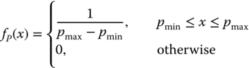
The variation of derating is manifested by parameter p in Eq. 3.5.6. The distribution of p can be appropriately extrapolated based on the actual derating of individual units. If p is uniformly distributed in a range of [pmin, pmax], its PDF, denoted as fP(x), can be expressed by
Note that pmin and pmax represent the smallest and the largest derating percentages, respectively. Now the mean and variance of πE can be estimated by

By considering the effects of temperature and derating variations in Eq. 3.5.4, the mean and variance of the component failure rate can be obtained as follows:
These moments along with the mean and variance of the non‐component failure rate in Eqs. 3.5.11 and 3.5.12 constitute the basic building blocks in DFR under six‐sigma criteria. This will be further elaborated in the case study of Section 3.9.
3.7 Fault‐Tree Method
3.7.1 Functional Block Diagram
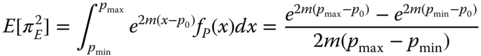
Building the functional black diagram (FBD) is the first step toward the analysis of the failure modes and root causes in the early product development phase. The FBD is a step‐by‐step procedure that describes the detailed functionality of a development process. As shown in Figure 3.20, the process consists of three sequential parts: Input, Process, and Output. Since the product is still in its early developmental phase, the steps identified under input, process, and output should not be too detailed. Each of these identified steps becomes a unique process that is later evaluated using a fault‐tree analysis (FTA). For that reason, three to five steps are usually sufficient to describe any input, process, or output in FBD.
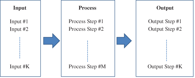
Figure 3.20A functional block diagram with input, process, and output parts.
The FBD shows that any output is the result of transforming the inputs via the immediate process. We use an air‐conditioning (A/C) system to illustrate this transformation process. When you turn on the switch of an A/C system, the electricity drawn from the grid flows into the electric motor coils to generate the electromagnetic field. That magnetic field drives the rotor and generate the torque. The torque further pushes the compressor such that the working fluid leaves the compressor and flows into the condenser, where the ambient hot air will exchange the heat with fluid and convert the fluid to low pressurized liquid. As the output or result of the process, the room temperature drops.
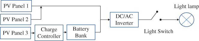
Let us use a roof-top solar PV system in Figure 3.21 to illustrate how to construct the FBD and further define input, process, and output steps. The schematic in the figure shows the components that make up a typical roof‐top PV system in a residential community. The system consists of a charger controller, battery bank, DC–AC inverter, light bulb (lamp), connecting wires, and two solar PV panels (more panels are installed in reality). The FBD begins with writing three high‐level labels: Inputs, Process, and Outputs. Hence the schematic diagram in Figure 3.21 should be used as an aid to identify each of the significant processes involved.
Figure 3.21Schematic diagram of a PV system with battery storage.
Identifying the input, process, and output are the necessary steps toward the FTA, which will be discussed next. As shown in Figure 3.22, we use the input of “turn on the light switch” as an example to illustrate how to proceed and detail the process steps. By turning the light switch on, it closes the electric circuit. It is then expected that current flows from the PV panels to the lamp filament via the DC–AC inverter. Since PV modules generate DC power, it needs to be converted into AC power before heating the lamp filament. This process happens during the daytime when the sun is available. In the night, since there is no sun, the power will flow from the battery to the lamb filament. Since the battery also stores DC energy, it needs to be converted into AC as well. Once the filament is heated, it generates the light that shines the room, which is the expected output. Now we are ready to perform the FTA based on the identified input, process, and output steps in the FBD.

Figure 3.22Functional block diagram of a roof‐top PV system.
3.7.2 Fault‐Tree Analysis
The FTA is a logical, graphical diagram that describes the interactions between failure modes and their causes. The diagram is constructed upon the preliminary analysis of input, process, and output steps of the FBD. Particularly, the FTA diagram hierarchically shows all failures for a system, subsystem, assembly, and module down to an individual component. The FTA oftentimes starts from a consideration of the system failure effects, referred to as “top events,” and the analysis proceeds by determining how these can be caused by individual or combined failure or events from lower‐level subsystems or components. Standard logic symbols are often used to construct an FTA diagram to capture the logical connections between individual events or components. Basic logics symbols that are commonly used are shown in Figure 3.23. The results of the FTA can then be transferred to an FMECA spreadsheet with which the failure modes and their causes are assessed in terms of their effects on the system design. This section illustrates how to construct an FTA diagram for failure analysis, and FMECA will be discussed in Section 3.8.

Figure 3.23Standard logic symbols used in fault‐tree analysis.
Let us construct the FTA diagram based on the FBD of the solar PV system shown in the previous section. The FTA shown in Figure 3.24 has two PV panels that generate the power in parallel. The top event failures of this system can be caused by either no current from the PV panels or from the battery bank; hence a two‐input OR gate captures this logic relation. At the next lower level (on the left side), any failure of the charge controller, DC–AC inverter, and two PV modules cause a shortage in the electricity supply; hence a three‐input AND gate is used. Since two PV modules are configured in parallel, there is no power generation only if both fail. The major uncontrollable event is the sun. Hence a three‐input OR gate is applied to represent this relation. In case the power is supplied through the stored energy in the night (see the right side), it requires that battery bank, DC–AC inverter, and switch all to be working. Thus a three‐input AND gate is used.

Figure 3.24FTA for the roof‐top PV system.
It is worth mentioning that each FTA diagram is constructed corresponding to a uniquely defined top event, which can be caused by different failure modes or logical connections between failure events. In the solar PV system, if the top event is “unsafe voltage,” then it would be necessary for the DC–AC inverter's voltmeter to be available, and gate G1 would have to be changed to an OR gate along with the output of current G1.
In addition to depicting the logical connections between failure events in relation to top‐level events, FTA can be used to estimate the top event probabilities, in the same way as in the reliability block diagram analysis in Chapter 02. Failure probabilities derived from reliability prediction models or simulation programs can be assigned to the failure events, and cut set and path set methods can be applied to evaluate system failure probability.
3.8 Failure Mode, Effect, and Criticality Analysis
3.8.1 Priority Risk Number
Failure mode, effect, and criticality analysis (FMECA) is perhaps the most widely used reliability analysis and improvement method in product design. The principle of FMECA is to analyze each failure mode of individual components and to determine the effects of system‐level operation of each failure mode. FMECA may be performed at a functional level or on a piece part (i.e. hardware). Functional FMECA studies the effects of failure at the reliability block level, such as a power supply of a microprocessor. Hardware FMECA investigates the effects of failures of individual components, such as relays, resistors, valves, or bearings. Since actual hardware failure modes are investigated (e.g. resistor short circuit, broken solder joint), a hardware FMECA is able to provide the detailed estimates of failure probabilities, but requires far more effort. However, functional FMEA can be performed much earlier when hardware items have not been uniquely identified in a product concept phase or when hardware is not fully defined. Therefore, hardware and functional FMECAs are complementary, and an FMECA can also be performed using a combination of hardware and functional approaches. Table 3.10 shows the typical failure modes of resistors and relays, where α is the ratio of a particular failure mode of the component occurring in field products.
Table 3.10 Failure mode types and ratios of resistor and replays.
| Component | Failure mode | α | Component | Failure mode | α |
| Resistor | Parameter shift | 0.70 | Relay | Fail to trip | 0.55 |
| Open circuit | 0.27 | Spurious trip | 0.16 | ||
| Short circuit | 0.03 | Relay stuck | 0.24 |
Figure 3.25 shows a typical FMECA worksheet taken from the Automotive Industry Action Group (ReliaSoft 2017). Method 101 is a non‐quantitative method, which serves to highlight failure modes whose effects would be considered important in relation to severity, detectability, safety, or maintainability.

Figure 3.25A typical FMECA spreadsheet.
RAC CRTA‐FMECA and MIL‐HDBK‐338 both identify Risk Priority Number (RPN) calculations as an alternate method to criticality analysis. The RPN is defined as follows:
where D, S, and O each is on a scale from 1 to 10. The highest RPN is 10 × 10 × 10 = 1000, meaning that this failure is not detectable by inspection, is highly severe, and the occurrence is almost certain. If O = 1, the RPN decreases to 100. Hence the criticality analysis guides the focus on the highest failure risks.
3.8.2 Criticality Analysis
Criticality analysis includes consideration of the failure rate or probability, the failure mode ratio, and a quantitative assessment of criticality, in order to provide a quantitative rating of the criticality for the component or function. The failure mode criticality number is
where
| β | = | conditional probity of losing function or mission |
| α | = | failure mode ratio (for an item sum of all α = 1) |
| λp | = | part failure or hazard rate |
| t | = | operating or at‐risk time of item |
The expected number of failures λpt can be replaced by the failure probability (1 − exp(−λpt)). The item criticality number is the sum of the failure mode criticality numbers for the item under study.
In practice, when performing FMECA for quality and reliability assurance, interdependencies among various failure modes with uncertain or imprecise information are very difficult to incorporate into the assessment measure. Thus, methods like the Markov chain and fuzzy logistic are considered to be an effective tool to address the correlations of different failure modes or components (Xu et al. 2002; Xiao et al. 2011).
A system may be subject to a common cause failure (CCF), where the failure of multiple components is the result of a shared event or coupling factor (or mechanism). In fact, studies have shown that CCF events may account for between 20% and 80% of the unavailability of safety systems within nuclear reactors (Werner 1994). In addition, the CCF effect is a stochastic and time‐varying process due to the influence of various degradation mechanisms, such as wear, corrosion, and fatigue (Fan et al. 2018). However, it is generally agreed that CCF does not include those multiple component failures because of a functional dependency that is modeled in a traditional fault tree or system reliability model (Wu et al. 2011). In particular on redundant systems, reliability dependency exists between components that are provided by the same company, or maintained by the same technician, or a reliability estimation derived from the same test sample.
3.9 Case Study: Reliability Design for Six Sigma
3.9.1 Principle of Design for Six Sigma
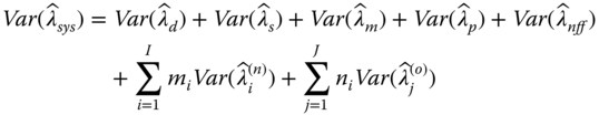
The design for Six Sigma (DFSS) emerged from the Six Sigma quality control and the Define‐Measure‐Analyze‐Improve‐Control (DMAIC) methodologies (ReliaSoft 2017). Though the primary goal of DFSS is to take proactive measures to reduce the number of non‐conforming units at an early design and manufacturing stage, reliability also plays an important role in terms of achieving the MTBF target, meeting the safe requirement, and achieving customer satisfaction. In this section, we introduce a DFSS‐based reliability design methodology to proactively address the long‐term (post‐installation) reliability issues in the early design and development phase. A generic system failure rate model that incorporates both component and non‐component failures is given as follows:
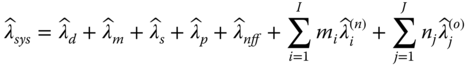
where
| = | failure rate of design issues | |
| = | failure rate of manufacturing defects | |
| = | failure rate of software bugs | |
| = | failure rate of process issues | |
| = | failure rate of NFF issue | |
| I | = | number of new component types |
| J | = | number of existing component types |
| = | failure rates of new component type i, for i = 1, 2, …, I | |
| = | failure rates of existing component type j, for j = 1, 2, …, J | |
| mi | = | number of units of component type i used in the system |
| ni | = | number of units of component type j used in the system |
In Eq. 3.9.1, the first five terms represent the non‐component failure rates, which include design, manufacturing, software, process, and NFF. The last two terms capture the aggregate failure rate of all hardware components. Particularly, ![]() represents the failure rate of new components used in the design and
represents the failure rate of new components used in the design and ![]() represents the failure rate of components used in predecessor products. Section 3.5.4 showed how to estimate failure rates of new and existing component types due to the different life data source.
represents the failure rate of components used in predecessor products. Section 3.5.4 showed how to estimate failure rates of new and existing component types due to the different life data source.
Reliability uncertainties are caused by various factors, such as design changes, limited test time, temperature and electrical derating variations, and customer usage, among others. Though the exact distribution for ![]() is difficult to obtain, the mean and the variance of
is difficult to obtain, the mean and the variance of ![]() can be estimated as follows:
can be estimated as follows:

Both Eqs. 3.9.2 and 3.9.3 are derived by assuming that failures of components and non‐components are mutually independent. Since ![]() ,
, ![]() ,
,![]() ,
, ![]() ,
, ![]() ,
, ![]() , and
, and ![]() are uniformly bounded, according to the central limit theorem (CLT),
are uniformly bounded, according to the central limit theorem (CLT), ![]() tends to be normally distributed for large values of component numbers. The system failure rate with (1 − α) × 100% confidence can be estimated by
tends to be normally distributed for large values of component numbers. The system failure rate with (1 − α) × 100% confidence can be estimated by
where Z1−α is the z‐value of the standard normal distribution. Given the mean and variance of ![]() , the product reliability can also be specified by the MTBF with a predefined convergence. That is,
, the product reliability can also be specified by the MTBF with a predefined convergence. That is,
where MTBF is the target mean‐time‐between‐failure of the system. Different confidence levels of the product MTBF are desirable before volume manufacturing begins. The lower bound of MTBF can be improved by using more reliable components, lowering the operating temperature, or reducing the derating percentage, or enhancing the design, software testing, manufacturing quality, and processes.
3.9.2 Implementation of Printed Circuit Board Design
In this section, the proposed DFSS model in Eq. 3.9.5 is applied to design a new printed circuit board (PCB) assembly. The board consists of 54 component types with a total of 759 parts. Seven new component types (with a total of 119 parts) are first used in the board. Since no field failure data are available for new components, their failure rates are extrapolated based on the methods described in Section 3.6. Table 3.11 presents the temperature and electrical derating parameters of seven new components. The activation energy Ea and fitting parameter m can be obtained from component suppliers or found in technical handbooks such as Bellcore SR‐332. In industry, FIT is often used instead of failure rate. FIT is defined as the number of failures in 109 hours. For example, the FIT of 1 MB EPROM is 77.4, which is equivalent to a failure rate of 7.74 × 10⁻⁸ faults per hour (i.e. 77.4/109). The other 47 component types have been used on predecessor products. Therefore their failure rates can be directly calculated using Eq. and the results are summarized in Table 3.12.
Table 3.11 Data for estimating failure rates of new components.
Source: Reproduced with permission of IEEE.
| Input data | Output data | ||||||||||||
| i | Component name | ni | FIT | Ea | μT | σT | u | v | m | ||||
| 1 | 1 MB EPROM | 14 | 37.4 | 1.4 | 43.7 | 1.7 | 60 | 80 | 0.024 | 1.90 | 0.53 | 1.63 | 1.04 |
| 2 | 0.2 W 1% Resistor | 32 | 3.33 | 1.2 | 47.6 | 8.3 | 50 | 70 | 0.019 | 5.08 | 7.11 | 1.22 | 0.53 |
| 3 | FPGA | 26 | 6.1 | 0.7 | 56.2 | 4.1 | 60 | 85 | 0.024 | 3.74 | 1.16 | 1.74 | 1.18 |
| 4 | Switch transistor | 26 | 5.81 | 1.2 | 51.8 | 2.8 | 60 | 75 | 0.024 | 5.37 | 2.03 | 1.53 | 0.91 |
| 5 | Op amp | 3 | 9.00 | 1.2 | 46.6 | 5.2 | 55 | 75 | 0.024 | 3.17 | 2.46 | 1.45 | 0.83 |
| 6 | Clock driver | 14 | 0.823 | 1.2 | 65.1 | 1.9 | 65 | 80 | 0.024 | 27.86 | 6.51 | 1.73 | 1.13 |
| 7 | Switch diode | 4 | 11.25 | 1.0 | 63.2 | 6.4 | 60 | 80 | 0.029 | 15.74 | 11.08 | 1.81 | 1.25 |
Table 3.12 Data for failure rate of existing components.
Source: Reproduced with permission of IEEE.
| i | Comp type | ni | FIT | i | Comp type | ni | FIT | i | Comp type | ni | FIT |
| 8 | comp 1 | 16 | 130 | 24 | comp 17 | 1 | 3.643 | 40 | comp 33 | 2 | 0.823 |
| 9 | comp 2 | 10 | 5.23 | 25 | comp 18 | 1 | 3.643 | 41 | comp 34 | 1 | 1.029 |
| 10 | comp 3 | 10 | 10.00 | 26 | comp 19 | 1 | 3.643 | 42 | comp 35 | 1 | 1.00 |
| 11 | comp 4 | 10 | 5.23 | 27 | comp 20 | 1 | 3.33 | 43 | comp 36 | 1 | 1.00 |
| 12 | comp 5 | 1 | 10.00 | 28 | comp 21 | 4 | 0.823 | 44 | comp 37 | 1 | 0.823 |
| 13 | comp 6 | 9 | 1.029 | 29 | comp 22 | 4 | 0.823 | 45 | comp 38 | 1 | 0.823 |
| 14 | comp 7 | 1 | 9.00 | 30 | comp 23 | 4 | 0.823 | 46 | comp 39 | 1 | 0.823 |
| 15 | comp 8 | 9 | 0.823 | 31 | comp 24 | 4 | 0.823 | 47 | comp 40 | 1 | 0.823 |
| 16 | comp 9 | 2 | 3.643 | 32 | comp 25 | 3 | 0.823 | 48 | comp 41 | 1 | 0.823 |
| 17 | comp 10 | 2 | 3.643 | 33 | comp 26 | 3 | 0.823 | 49 | comp 42 | 1 | 0.823 |
| 18 | comp 11 | 8 | 0.823 | 34 | comp 27 | 2 | 1.029 | 50 | comp 43 | 1 | 0.823 |
| 19 | comp 12 | 8 | 0.823 | 35 | comp 28 | 2 | 1.00 | 51 | comp 44 | 252 | 0.000 05 |
| 20 | comp 13 | 6 | 1.029 | 36 | comp 29 | 2 | 0.823 | 52 | comp 45 | 24 | 0.0004 |
| 21 | comp 14 | 7 | 0.823 | 37 | comp 30 | 2 | 0.823 | 53 | comp 46 | 177 | 0.000 05 |
| 22 | comp 15 | 6 | 0.823 | 38 | comp 31 | 2 | 0.823 | 54 | comp 47 | 6 | 0.0002 |
| 23 | comp 16 | 6 | 0.823 | 39 | comp 32 | 2 | 0.823 |
Reliability of non‐components is estimated from three predecessor products with similar complexity, namely PCB‐A, PCB‐B, and PCB‐C, and the triangular distribution parameters {a, b, c} are obtained and listed in Table 3.13. By combining data in Tables 3.11–3.13, we are able to calculate the mean and variance of PCB's failure rate using Eqs. 3.9.2 and 3.9.3, respectively. The E[λPCB] = 1.08 × 10⁻⁵ and Var(λPCB) = 3.3 × 10⁻¹² are shown in Table 3.14. The detailed computation is automated in Matlab. Based on Eq. , the lower bound of MTBF for the new design is also obtained as 63 000 hours with 99.7% confidence.
Table 3.13 Triangular distribution parameters for non‐component failure rates.
Source: Reproduced with permission of IEEE.
| Input data (FIT) | Output data (faults/hour) | |||||
| PCB‐A | PCB‐B | PCB‐C | a (×10−7) | b (×10−7) | c (×10−7) | |
| Design errors | 148.5 | 423.6 | 855.0 | 1.49 | 8.55 | 4.24 |
| Software bug | 29.7 | 145.3 | 95.0 | 0.297 | 1.45 | 0.950 |
| Manufacturing | 207.9 | 242.1 | 285.0 | 2.08 | 2.85 | 2.42 |
| Process | 118.8 | 302.6 | 665.0 | 1.19 | 6.65 | 3.03 |
| Others (NFF) | 475.3 | 641.5 | 807.5 | 4.75 | 8.08 | 6.42 |
Table 3.14 Mean and variance of failure rates for the new PCB assembly.
Source: Reproduced with permission of IEEE.
| Root case category | Components | Non‐component | System | |||||
| New comps | Existing comps | Design | Software | Mfg | Process | NFF | PCB | |
| mean | 6.52 × 10⁻⁶ | 2.42 × 10⁻⁶ | 4.76 × 10⁻⁷ | 9.0 × 10⁻⁸ | 2.45 × 10⁻⁷ | 3.62 × 10⁻⁷ | 6.41 × 10⁻⁷ | 1.08 × 10⁻⁵ |
| variance | 2.42 × 10⁻¹² | 0 | 2.47 × 10⁻¹³ | 8.66 × 10⁻¹⁵ | 6.07 × 10⁻¹⁴ | 1.44 × 10⁻¹³ | 4.16 × 10⁻¹³ | 3.30 × 10⁻¹² |
References
- Bei, X., Chatwattanasiri, N., Coit, D.W., and Zhu, X. (2017). Combined redundancy allocation and maintenance planning using a two‐stage stochastic programming model for multiple component systems. IEEE Transactions on Reliability 66 (3): 950–962.
- Bellcore, (1995), Reliability Prediction Procedure for Electronic Equipment, SR‐332, Issue 5, December 1995.
- Bowles, J.B. and Pelaez, C.E. (1995). Application of fuzzy logic to reliability engineering. Proceedings of the IEEE 83 (3): 435–449.
- Bulfin, R.L. and Liu, C.Y. (1985). Optimal allocation of redundancy components for large systems. IEEE Transaction on Reliability, vol. 34 (August): 241–247.
- Chern, M.S. (1992). On the computational complexity of reliability redundancy allocation in a series system. Operations Research Letter 11 (6): 309–315.
- Coit, D.W. and Liu, J. (2000). System reliability optimization with k‐out‐of‐n subsystems. International Journal of Reliability, Quality and Safety Engineering 7 (2): 129–142.
- Coit, D.W. and Smith, A.E. (1998). Redundancy allocation to maximize a lower percentile of system time‐to‐failure distribution. IEEE Transactions on Reliability 47 (1): 79–87.
- Coit, D.W., Jin, T., and Wattanapongsakorn, N. (2004). System optimization considering component reliability estimation uncertainty: multi‐criteria approach. IEEE Transactions on Reliability 53 (3): 369–380.
- Elsayed, E. (2012). Reliability Engineering, 2e. Hoboken, NJ: Wiley and IEEE Press.
- Fan, M., Zeng, Z., Zio, E. et al. (2018). A stochastic hybrid systems model of common‐cause failures of degrading components. Reliability Engineering and System Safety 172: 159–170.
- Fyffe, D.E., Hines, W.W., and Lee, N.K. (1968). System reliability allocation problem and a computational algorithm. IEEE Transactions on Reliability 17 (June): 64–69.
- Ghare, P.M. and Taylor, R.E. (1969). Optimal redundancy for reliability in series system. Operations Research 17 (September): 838–847.
- Guan, H., Chen, W.‐R., Huang, N., and Yang, H.‐J. (2010). Estimation of reliability and cost relationship for architecture‐based software. International Journal of Automation and Computing 7 (4): 603–610.
- Hadipour, H., M. Amiri, M. Sharifi, (2018) “Redundancy allocation in series‐parallel systems under warm standby and active components in repairable subsystems,” Reliability Engineering and System Safety, www.sciencedirect.com, available online 31 January 2018.
- Heydari, M. and Sullivan, K.M. (2018). An integrated approach to redundancy allocation and test planning for reliability growth. Computers and Operations Research 92 (4): 182–193.
- Holland, J.H., (1975), Adaptation in Natural and Artificial Systems, PhD Dissertation, University of Michigan Press, Ann Arbor, MI.
- Huang, H.‐Z., Liu, H.‐J., and Murthy, D.N.P. (2007). Optimal reliability, warranty and price for new products. IEEE Transactions 39 (8): 819–827.
- Hwang, C.L., Tillman, F.A., and Kuo, W. (1979). Reliability optimization by generalized lagrangian‐function and reduced‐gradient methods. IEEE Transactions on Reliability 28 (4): 316–319.
- IEEE, (1998), IEEE Standard Methodology for Reliability Prediction and Assessment for Electronic System and Equipment. IEEE Standard 1413, New York.
- Jia, H., Ding, Y., Peng, R., and Song, Y. (2017). Reliability evaluation for demand‐based warm standby systems considering degradation process. IEEE Transactions on Reliability 66 (3): 795–805.
- Jiang, R. and Murthy, D.N.P. (2009). Impact of quality variations on product reliability. Reliability Engineering and System Safety 94 (2): 490–496.
- Jin, T., P. Su, (2005), “Minimize system reliability variability based on six‐sigma criteria considering component operational uncertainties”, in Proceedings of Annual Reliability and Maintainability Symposium, pp. 214–219.
- Jin, T., Taboada, H., Espiritu, J., and Liao, H. (2017). Allocation of reliability‐redundancy and spares inventory under Poisson fleet expansion. IISE Transactions 49 (7): 737–751.
- Konak, A., Coit, D.W., and Smith, A.E. (2006). Multi‐objective optimization using genetic algorithms: a tutorial. Reliability Engineering and System Safety 91 (9): 992–1007.
- Kuo, W. and Zuo, M.J. (2003). Optimal Reliability Modeling: Principles and Applications, 1e. Hoboken, NJ: Wiley.
- Kuo, W., Prassad, V.R., Tillman, F.A., and Hwang, C. (2001). Optimal Reliability Design: Fundamental and Applications, 1e. Cambridge, UK: Cambridge University Press.
- Levitin, G., Xing, L., and Dai, Y. (2017). Optimization of component allocation/distribution and sequencing in warm standby series‐parallel systems. IEEE Transactions on Reliability 66 (4): 980–988.
- Liang, Y.‐C. and Smith, A.E. (2004). An ant colony optimization algorithm for the redundancy allocation problem (RAP). IEEE Transactions on Reliability 53 (3): 417–423.
- Mettas, A., (2000), “Reliability allocation and optimization for complex systems,” in Proceedings of Reliability and Maintainability Symposium, pp. 216–221.
- Öner, K.B., Kiesmüller, G.P., and van Houtum, G.J. (2010). Optimization of component reliability in the design phase of capital goods. European Journal of Operational Research 205 (3): 615–624.
- Ozen, T.M. (1986). Applied Mathematical Programming for Production and Engineering Management. Prentice‐Hall.
- Pecht, M., Das, D., and Ramakrishnan, A. (2002). The IEEE standards on reliability program and reliability prediction methods for electronic equipment. Microelectronics Reliability 42 (2002): 1259–1266.
- ReliaSoft (2017), FMECA, http://www.weibull.com/hotwire/issue46/relbasics46.htm (accessed on February 28, 2017).
- Sayama, H., Kameyama, Y., Nakayama, J., and Sawaragi, Y. (1973). Iteration process in the Lagrange multipliers for multiplier method. System and Control (Japan) 17: 775–778.
- Sinaki, G., (1994), Ultra‐reliable fault tolerant inertial reference unit for spacecraft. Advances in the Astronautical Sciences 86: 239–248.
- Sung, C.S. and Cho, Y.K. (1999). Branch‐and‐bound optimization for a series system with multiple‐choice constraints. IEEE Transactions on Reliability 48 (2): 108–117.
- Taboada, H.A., Espiritu, J.F., and Coit, D.W. (2008). MOMS‐GA: a multi‐objective multi‐state genetic algorithm for system reliability optimization design problems. IEEE Transactions on Reliability 57 (1): 182–191.
- Teng, J.T. and Thompson, G.L. (1996). Optimal strategies for general price‐quality decision models of new products with learning production costs. European Journal of Operational Research 93 (3): 476–489.
- US MIL‐HDBK‐217 (1995). Reliability prediction for electronic systems. In: Available from National Technical Information Service. VA: Springfield.
- Werner, W. (1994). Results of recent risk studies in France, Germany, Japan, Sweden and the United States. Paris: OECD Nuclear Energy Agency, NEA/CSNI/R.
- Wu, J., Yan, S., and Xie, L. (2011). Reliability analysis method of a solar array by using fault tree analysis and fuzzy reasoning Petri net. Acta Astronautica 69 (11/12): 960–968.
- Xiao, N., Huang, H.‐Z., Li, Y. et al. (2011). Multiple failure modes analysis and weighted risk priority number evaluation in FMEA. Engineering Failure Analysis 18 (4): 1162–1170.
- Xu, K., Tang, L.C., Xie, M. et al. (2002). Fuzzy assessment of FMEA for engine systems. Reliability Engineering and System Safety 75 (1): 17–29.
- Yeh, C.‐T. and Fiondella, L. (2017). Optimal redundancy allocation to maximize multi‐state computer network reliability subject to correlated failures. Reliability Engineering and System Safety 166 (October): 138–150.
Problems
Show that the cost function of Eq. 3.2.2 is an decreasing function with α, meaning db(α)/dα > 0. Also show that Eq. 3.2.2 is a convex function, meaning d2b(α)/dα2 > 0.
- Problem 3.2 Problem Show that c(α) in Eq. 3.2.3 is strictly decreasing and strictly convex in α.
- Problem 3.3 Problem Look at the data of Example 3.1. The analysis shows that Product A has a higher reliability gain than Product B if an additional budget of $5000 is allocated. If the total design budget is $25 000, do you prefer Product A or Product B?
- Problem 3.4 Problem Using the same data given in Example 3.2, do the following, assuming that the annual quantity of new product installation is Q = 2000/year: (1) find the optimal α* for T = 3 years and (2) find the optimal α* for T = 5 years (assuming that the annual discount factor is 10%).
- Problem 3.5 Problem (Reliability allocation) Given the total cost budget C = 50 000, find the optimal component reliability to maximize the reliability of the following two designs, respectively. The component reliability and cost data are given in Table 3.2. Solve the problem using iteration.

- Problem 3.6 Problem (Reliability allocation) Use the Lagrangian function to find the optimal component reliability in Problem 3.5 and compare the results obtained from the one based on iterations.
- Problem 3.7 Problem (Reliability allocation) Minimize the system cost in the two designs in Problem 3.4. For design 1, the minimum system reliability should not be less than 0.92. For design 2, the minimum system reliability should be higher than 0.88.
- Problem 3.8 Problem (Redundancy allocation) For a series system comprised of four subsystems, each subsystem is allowed to adopt parallel or redundant components to improve the overall reliability. The reliability and cost of each component choice is given in the table below. Given the total system cost budget is 15: (1) maximize the system reliability assuming only one component type is selected for each subsystem; (2) maximize the system reliability with no constraints on component types per subsystem.
Component reliability and cost.
Component type j = 1 Component type j = 2 Subsystem i Reliability (rij) Cost (cij) Reliability (rij) Cost (cij) 1 0.90 1 0.95 2 2 0.88 2 0.92 3.5 3 0.86 1.5 0.91 3 4 0.85 0.5 0.93 2.5 - Problem 3.9 Problem (Redundancy allocation) For the same series system in Problem 3.8, we want to minimize the cost subject to the system reliability requirement. Assuming the system reliability must be above 0.97: (1) minimize the system cost assuming only one component type is selected for each subsystem; (2) minimize the system cost with no constraints on component types per subsystem.
- Problem 3.10 Problem Solve Example 3.5 using the heuristic method. The heuristic rule is given as follows: to maximize the reliability of a series system via redundant units, we want to maximize the reliability of each subsystem as the system reliability is the product of subsystem reliability.
- Problem 3.11 Problem (Allocation of k‐out‐of‐n subsystems) Use the same reliability and cost data in Table 3.4 to perform the k‐out‐of‐n redundancy allocation. The component failure rates for HSD, DC, Analog, and MW are 0.000 02, 0.000 025, 0.000 05 and 0.0001 failures/hour, respectively. The system reliability upon 1000 hours is required to be 0.8: find the optimal x* that minimize the system cost. Solve this problem in two cases: (1) assuming all redundant components are in hot‐standby mode; (2) redundant components are in cold‐standby mode.
- Problem 3.12 Problem (Multicriteria design) Using the data in Table 3.5 and C = 29 and W = 45, find the Pareto optimal solutions for Model 3.8 to maximize the system reliability and minimize the reliability variance.
- Problem 3.13 Problem (Multicriteria design) Solve Model 3.8 again using the same data in Problem 3.11 on the condition that for each subsystem only one component type is chosen.
- Problem 3.14 Problem (Multicriteria design) Solve Model 3.8 again using the same data in Problem 3.11 on the condition that for each subsystem only one component type is chosen.
- Problem 3.15 Problem Assume that a solar park has 10 000 solar PV panels. Each panel is installed with one DC–AC inverter. In the last two years, 25 inverter failures are reported from the park. A failed inverter is replaced with a good unit so that the power generation is ensured. Assume that the system repair downtime is negligible compared to the uptime. Estimate the failure rate of the inverter.
- Problem 3.16 Problem The activation energy Ea of component A is 0.5 eV and the Ea of component B is 0.7 eV. If component B operates at 70 °C, at what temperature can component A operate such that it has the same πT as component B?
- Problem 3.17 Problem Based on the fitting parameter m in Table 3.9, plot the electrical derating factor πE for a 0.2 W 1% resistor and operational amplifier as p increases from 50% to 100%.
- Problem 3.18 Problem For a triangle distribution with parameters a, b, and c for the lowest, medium, and largest values, respectively, prove the mean and the variance are

- Problem 3.19 Problem Given the uniform PDF of p in Eq. 3.6.8, prove that Eqs. 3.6.9 and 3.6.10 are the actual mean and the second moment of πE.
- Problem 3.20 Problem The mean failure rate of a PCB module is 1.5 × 10⁻⁵ failures/hour and the standard deviation of the failure rate is 4.5 × 10⁻⁶ failures/hour. Estimate the MTBF at the 90 and 99% confidence levels, respectively.
- Problem 3.21 Problem A simple solar PV system is shown below. Create the functional block diagram for this system and perform FTA based on the functional diagram.