
Chapter 16
Preamplifier 2012
Part 3: level indicator, source selector, power supply (Elektor, June 2012)
This is the third and final article on Preamplifier 2012, covering the level indication circuitry, the input selection system, and the power supply.
The Log Law Level LED, or LLLL, was thought up to help with the correct setup of phono input with switched gain options. It is, to the best of my knowledge, a new idea. A single LED level driven by a comparator typically goes from fully off to fully on for less than a 2 dB change in level when measuring actual music rather than steady sinewaves. The LLLL also uses a comparator to drive the indicating LED hard on or hard off, but before that is a simple log-converter so that the level range from LED always-off to always-on is much increased, to about 10 dB with music. The on-off ratio indicates where the level lies in that range. It is straightforward to set it up so that the level is correct when the LED is on about 50% of the time. This gives a much better indication than simple comparator methods.
In this application, a stereo version of the LLLL is required; it would be possible to use separate LLLL’s for each channel, but this hardly seems necessary. The version chosen uses a single LED to indicate the greater of the two input signals, and there are two rectifier and log-converter sections, with the output of comparator IC5A (Left) wire-OR’ed with the output of IC5C (Right). Looking at this approach with the famed clarity of hindsight, a more elegant and economical way to make a stereo version would be to combine the outputs of the two peak rectifiers IC1A, IC1B and IC3A, IC3B to charge a single capacitor C2. This would save a good number of components as there is now only one log-converter and one comparator. I must confess that I have not yet got around to actually trying it out, but it looks solid.
The Preamplifier 2012 was originally designed with a rotary switch for input selection. Elektor replaced this with a relay system. Relays are also used to select between MM and MC inputs, to switch the IEC Amendment in and out, and to switch the tone-control in and out. The switched-gain stage is not controlled by relays; the gain option is selected by a jumper.
The power supply is completely conventional, using LM317 and LM337 IC regulators. A well-designed opamp preamplifier with a competent grounding system does not require very low levels of supply-rail noise and this power supply is more than adequate for the task. Elektor added the 7815 regulator IC3 to power the relays.
Elektor produced a suite of PCBs for the Preamplifier 2012. The circuitry was split into the phono board, the balanced-input/tone-control/volume-control board, the LLLL board, the PSU, a board holding rotary switches to control the relay system, and two input/output connector boards.
Elektor are unusual in that when they publish a project, they measure it exhaustively in their own laboratories. I am glad to report that the results were entirely in line with my own measurements. Some of the Elektor measurements were published at the end of the first article.
Preamplifier 2012
This month we close off the discussions of the individual boards that make up the preamplifier, both in terms of theory of operation and construction.
The Log-Law Level LED (LLLL) stage
The Log Law Level LED, or LLLL, is to the best of my knowledge, a new idea. A normal single-LED level indicator is driven by a comparator, and typically goes from fully-off to fully-on with less than a 2 dB change in level when fed with music (not sine waves). It therefore does not give much information. The LLLL, on the other hand, incorporates a simple logarithmic converter so the range from LED-always-off to LED-always-on is extended to 10 dB. The preamplifier internal level is correct when the LED is on about 50% of the time. This gives a much better indication as you can judge the level approximately from the on/off ratio.
Referring to the circuit diagram in Figure 16.1, IC1A with R1, R2, D1, D2 is a precision half-wave rectifier circuit. Its output when combined with the feed through R3 provides a full-wave rectified signal to IC1B; this is another precision rectifier that establishes the peak level of the signal on C2. This is buffered by IC2A to prevent loading by the next stage, and the peak voltage is applied to the very simple log-law converter IC2B. For low level signals the gain is set to unity by R6 and R7. As the input voltage increases, first D5 begins to conduct, reducing the gain of the stage by increased negative feedback through R8. At a higher voltage set by divider R9 and R10, D6 also conducts, reducing the gain further by negative feedback through R9. This simple circuit clearly gives only a very approximate version of a log law but it transforms the operation of the indicator.
The processed voltage is applied to comparator IC5A, and if the threshold set by R21, R22 is exceeded the open-collector output of IC5A goes Low and the output of IC5B, which simply acts as a logical inverter, goes High, removing the short across the LED connected to pinheader K6 and allowing it to be powered by current source T1. There are two channels for stereo operation and the outputs of comparators IC5A and IC5C are wire-OR’d together to pull-up resistor R23 so that a signal on either channel will make the LED illuminate. IC5D is not used. The LLLL can be switched to read either the phono input directly (so the switched-gain stage can be set up correctly) or the signal after the input select relays and balanced line input stage, where it can be used to check the incoming level of any input. This switching is done by relay contacts RE1B, RE1C. Series relay contacts RE2B, RE2C allow the LLLL to be disabled when its job is done and the flickering LED may become irritating.
The LLLL is built on circuit board no. 110650–6 shown in Figure 16.2. It contains through-hole components only, hence nothing should hinder you from producing a working board straight off if you are careful about placing and soldering the parts. The same applies to the other three (four) boards discussed below. The finished LLLL board is pictured in Figure 16.3.

Figure 16.1
Schematic of the Log-Law Level LED (LLLL) board.
LLLL Board (# 110650–6)
Resistors
(0.25W, 1%)
R1,R2,R3,R5,R11,R12,R13,R15 = 20kΩ
R4,R6,R7,R14,R16,R17 = 10kΩ
R8,R9,R18,R19 = 1kΩ
R10,R20 = 100kΩ
R21 = 910Ω
R22,R23,R25 = 22kΩ
R24 = 100Ω
R26,R27 = 220Ω
Capacitors
C1-C4 = 2.2µF 20% 100V, diam. 6.3mm, 2.5mm pitch
C5-C9 = 100nF 10% 100V, 7.5mm pitch
C10,C11 = 100µF 20% 25V, diam. 6.3mm, 2.5mm pitch
C12,C13 = 220nF 10%, 100V, 7.5mm pitch
Inductors
L1,L2 = 1mH 3.6Ω 370mA, axial
Semiconductors
D1-D14 = 1N4148
T1 = BC557B
IC1-IC4 = NE5532
IC5 = LM339
Miscellaneous
K1-K4,K6 = 2-pin pinheader, 0.1” pitch (2.54mm)
Socket headers for K1-K4,K6
K5 = 3-pin pinheader, 0.1” pitch (2.54mm)
Socket header for K5
K7 = 3-way PCB terminal block, 5mm pitch
RE1,RE2 = V23105-A5003-A201, 12V/960Ω, 230V/3A, DPDT
PCB # 110650–6 (www.elektorpcbservice.com)
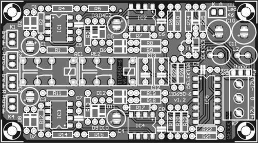
Figure 16.2
The combined metering and driver circuitry of the Log-Law Level LED indicator is built on this board. Board available through www.elektorpcbservice.com.

Figure 16.3
Prototype of the LLLL board built by Elektor Labs.
The input PCBs
The input circuit boards (one per channel) carry the input and output connectors plus the relays that select which input is in use. Their circuit diagram appears in Figure 16.4. The four line-level inputs can work in either unbalanced or balanced mode, though of course balanced mode is strongly recommended because it rejects electrical noise on the ground paths. Bear in mind this is true even if the source is unbalanced. In this case the cold (phase-inverted) balanced input must be connected to ground at the source end of the cable—a 3-way cable is still required. There is therefore no technical reason to provide RCA connectors but they are included for convenience. If they are to be used the jumpers JP1–JP4 must be installed.
For Input 1, relay contacts RE1B, RE1C connect to the preamplifier input when relay coil RE1A is energized, and the signal goes to the main preamplifier board via connector K15.
Facilities are also provided for using the XLR inputs in unbalanced mode; in this case the jumper S1 is set so that RE1B connects to ground rather than pin 3 of the XLR. The same applies to Input 2 and Input 3. However, if you have spent the money for an XLR you really should make proper use of it by employing balanced mode.
Input 4 is the phono input if the phono facility is included in the preamplifier. Input 4 is used for either MM or MC mode, as this selection is made on the phono PCB discussed in part 2. In this case K7 and K8 are not fitted. If the phono PCB is not used Input 4 can be used as another Line input, with K7 and K8 fitted. In this case there is no connection to K13.
There is no facility for using the MC and MM cartridge inputs in balanced mode so only RCA connectors are provided for these inputs.
This circuit is constructed on circuit board no. 110650–3 pictured in Figure 16.5; the assembled board appears in Figure 16.6.
The front panel PCB
The front panel board of which the schematic is shown in Figure 16.7, carries the input select switch, the LLLL source select switch, the three mode switches, and the power and LLL LEDs.
S5A is the input select switch, controlling the relays on the input boards Only the first four positions are used, the other two being blocked off by a mechanical stop. S5B is not used. The switching between MM/MC and Line input is done by a separate switch S2 on the front panel board.

Figure 16.4
Circuit diagram of the input section of the preamplifier.
S4A and S4B control the operation of the LLLL indicator. In the first position the LLLL is fed from after the input select and balanced input stage and can be used to check any input. In the second position it is fed from the phono stage only, whichever input is selected. The third position removes the signal fed to the LLLL and so disables it. Only the first three positions of the switch are used (Line—Phono—Off) and the other three are blocked off by a mechanical stop. Switch S1 controls the tone-control defeat relay. When S1 is closed the tone-control is bypassed completely.

Figure 16.5
The preamplifier’s input board (here at 75% of its real size). Two of these are required for stereo operation. Board available through www.elektorpcbservice.com.

Figure 16.6
Fully assembled Input board.
Component list
Input Board (#110650–3)
Resistors
R1,R2 = 0Ω
Capacitors
C1-C4 = 220nF 10% 100V, 7.5mm lead pitch
Miscellaneous
K1,K3,K5,K7 = XLR socket, PCB mount, horizontal, 3-way
K11 = XLR plug, PCB mount, horizontal, 3-way
K2,K4,K6,K8-K10,K12 = RCA/Phono socket, PCB mount, Pro Signal type PSG01545 (red) (R) or PSG01546 (white) (L)
K13,JP1-JP4 = 2-pin pinheader, 0.1” pitch (2.54mm)
Socket header for K13
K14,K15,K16 = 4-pin pinheader, 0.1” pitch (2.54mm)
Socket headers for K14,K15,K16
K17 = 10-way boxheader, straight, 0.1” pitch (2.54mm)
S1-S4 = 3-pin pinheader, 0.1” pitch (2.54mm)
Jumpers for S1-S4,JP1-JP4
RE1-RE4 = V23105-A5003-A201, 12V/960Ω, 230V/3A, DPDT
PCB # 110650–3 (www.elektorpcbservice.com); 2 pcs required
Switch S2 selects between moving-magnet (MM) and moving-coil (MC) operation, using relay contacts RE1B, RE1C on the phono PCB. When S2 is closed the MC input is active.
S3 selects the IEC amendment, which is a largely unwanted extra roll-off at 20 Hz that was later added to the RIAA spec. When S3 is closed the IEC amendment is applied. The small board no. 110650–4 for securing to the front panel of your preamplifier case is pictured in Figure 16.8, along with the Component List. Check Figure 16.9 for the assembled board.
The power supply PCB
The power supply is fairly conventional as the preamplifier does not require ultra-low noise on the supply rails to give its best performance. Referring to Figure 16.10, a center-tapped 18–0–18 V power transformer, a bridge rectifier D3–D6 and reservoir capacitors C8, C10 produce the unregulated supply voltages. Snubbing capacitors C14–C17 prevent RF being generated by the rectifier diodes. LEDs D7 and D8 are mounted on the PCB and indicate
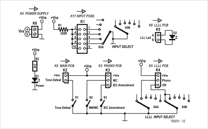
Figure 16.7
This sub circuit of switches, LEDs, resistors and connectors forms a separate board intended for fitting to the inside of the preamplifier front panel.
Component list
Front Panel Board (#110650–4)
Resistors
(0.25W, 1%)
R1 = 220Ω
R2 = 3.3kΩ
Semiconductors
D1 = LED, green, 3mm, through hole
D2 = LED, red, 3mm, through hole
Miscellaneous
K1 = 10-way boxheader, straight, 0.1” pitch (2.54mm)
K2,K5,D1,S1-S3 = 2-pin pinheader, 0.1” pitch (2.54mm)
Socket headers for K2,K5,D1,S1-S3
K3,K4 = 3-pin pinheader, 0.1” pitch (2.54mm)
Socket headers for K3,K4
K6 = 2-way PCB terminal block, 5mm pitch
S1,S2,S3 = switch, SPDT (On-On)
S4,S5 = 2-pole, 6-position rotary switch, PCB mount, e.g. Lorlin type CK1050
PCB # 110650–4 (www.elektorpcbservice.com)
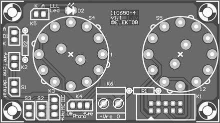
Figure 16.8
The front panel circuit board. Board available through www.elektorpcbservice.com.

Figure 16.9
The Front Panel board, ready for use.
that the unit is powered and both unregulated supplies are present. The ±17 V supplies for the opamps are generated by regulators IC1 and IC2. The networks R1, R2 and R3, R4 set the voltage required while C5 and C6 improve the ripple performance of the regulators. D1 and D2 prevent the stored charge on C5 and C6 damaging the regulators if the output is short-circuited. Capacitors C1-C4 reduce the output impedance of the supply at high frequencies.
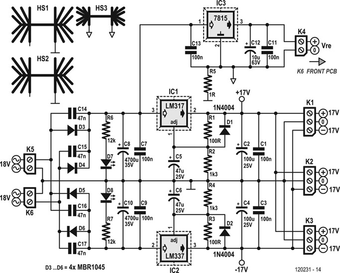
Figure 16.10
The circuit diagram of the power supply holds common-or-garden components hence few surprises. Note that the relays have their own 15 V voltage regulator.
A separate +15 V regulator IC3 is used to power the relays. This is powered from the unregulated positive supply that also feeds the +17 V regulator. Note that the audio ground and the relay ground must be connected together at one point only, right back at the power supply; otherwise relay currents flowing in the audio ground will cause unpleasant clicking noises in the preamp output.
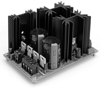
Number 110650–5 is the last board you’ll be building to construct the Preamplifier 2012; it’s shown in Figures 16.11 (PCB only) and 16. 12 (assembled board).
Wiring
Comprising a total of seven boards, the Preamplifier 2012 is quite an intricate job to wire up. For your convenience the connectors (‘Kx’) in this month’s schematics have been given what/where/to labels.
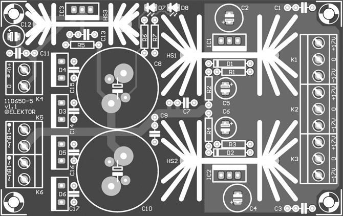
Figure 16.11
The power supply board. Board available through www.elektorpcbservice.com.

Figure 16.12
preamplifier PSU board assembled by Elektor Labs.
Power Supply Board (# 110650–5)
Resistors
(0.25W, 1%)
R1,R3 = 100Ω
R2,R4 = 1.3kΩ
R5 = 1Ω
R6,R7 = 12kΩ
Capacitors
C1,C3,C7,C9,C11,C13 = 100nF 10% 100V, 7.5mm pitch
C2,C4 = 100µF 20% 25V, 6.3mm diam., 2.5 mm pitch
C5,C6, = 47µF 20%, 25V, 6.3 mm diam., 2.5 mm pitch
C8,C10 = 4700µF 20% 35V, 22mm diam., 10mm pitch
C12 = 10µF 20% 63V, 6.3mm diam., 2.5mm pitch
C14-C17 = 47nF 50V, ceramic, 5mm pitch
Semiconductors
D1,D2 = 1N4004
D3-D6 = MBR1045
D7 = LED, red, 3mm, through hole
D8 = LED, green, 3mm, through hole
IC1 = LM317
IC2 = LM337
IC3 = 7815
Miscellaneous
K1,K2,K3 = 3-way PCB terminal block, 5mm pitch
K4,K5,K6 = 2-way PCB terminal block, 5mm pitch
HS1,HS2 = heatsink, 50.8 mm, Fischer Elektronik type SK 129 50,8 STS
HS3 = heatsink, 50.8 mm, Fischer Elektronik type SK 104 50,8 STS
PCB # 110650–5 (www.elektorpcbservice.com)
Not on PCB:
Tr1 = AC power transformer, 115/230V primary, 2×18V/50VA secondary, e.g. Multicomp # MCTA050/18, Farnell (Newark) # 9530380
F1 (230VAC) = fuse, 0.315A antisurge, 5×20mm, panel mount
F1 (115VAC) = fuse, 0.63A antisurge, 5×20mm, panel mount
S1 = 115/230V AC line voltage selector, e.g. Arcolectric Switches type T22205BAAC
S2 = AC power switch
Most of the board interconnections consist of short runs of 2, 3 or 4 light duty, flexible wires of different colors (agree on black for ground though) twisted together and their ends soldered to the socket for plugging on the pinheader. Look at the symbol with the mating pinheader on the PCB to identify the bevelled edge, this will help you get the pin-to-pin connections right.
The 10-way connection between the front panel PCB and the input PCB is the only one requiring a length of flatcable (a.k.a. ribbon cable) with IDC sockets pressed on at the ends.
All wiring and components ‘ahead of’ and including power transformer Tr1 is at AC powerline potential hence should comply with safety regulations and recommendations in place for electrical safety. When in doubt, ask for help or advice from a qualified electrician.
At the time of writing the Preamplifier 2012 is fully wired up on the audio test bench at Elektor House, but not yet fitted in a case. The two input boards are mounted like a sandwich using four PCB pillars. Depending on your response to the project we may do a final article later this year on installing the boards in a high quality enclosure. For now we leave that part of the project to you, as well as enjoying the superb sound quality of the Preamplifier 2012.