
Chapter 1
Advanced preamplifier design
A no-compromise circuit with noise gating (Wireless World, November 1976)
This was my first preamplifier design, conceived in 1975, the first year that I worked in the audio industry. The two gain-control solution to the dynamic-range problem was inspired by what was thought of as advanced industry practice at the time—notably in products by Radford and Cambridge Audio. I thought the rumble-gate concept was rather clever, but I seem to have been in a minority of one, as it was never even mentioned in the correspondence that followed. That was rather a disappointment.
The major part of the circuitry consisted of two discrete opamps with differential inputs, which performed the amplification and tone-control functions. The ±24V supply rails, which permitted a maximum signal level of about 16 Vrms, were provided by two 7824 IC regulators. The Moving Magnet (MM) input stage, however was a simple three–transistor stage running between +24 V and 0V. The reasoning was that in the MM stage low noise was the priority, the low signal levels making distortion much less of an issue, and so it was better to have a single input transistor rather than a differential pair; I had a vague notion that the pair would be 3 dB noisier. This is not actually the case, as the transistor of the pair that handles the negative feedback works under much better conditions for low noise than the input transistor, which is faced with the highly inductive source impedance of an MM cartridge. I have not yet got around to quantifying the difference, but clearly two devices must be noisier than one to some extent; having said that, the 5534 opamp with its differential inputs gives a very acceptable noise performance as an MM input stage. I later developed a more advanced discrete MM stage that had still only one input transistor, but could have been run between the +24V and −24V rails, giving a theoretical 6 increase in headroom. This approach is fully described in Chapter 2.
As shown in the block diagram (Preface Figure 1.2) the RIAA equalisation was divided into two halves. The HF roll-off at 2.1 kHz was implemented in the first stage, and the feedback around the normalisation amplifier implemented the boost starting at 500 Hz and levelling off at 50 Hz. Doing it this way round avoids a massive loss of headroom in the first stage [1], though at the cost on some compromise on noise. Splitting up the equalisation of course makes the RIAA component calculations very much easier, and unless I’m very much mistaken that is the inglorious and only reason that the idea has the popularity it does. That was not the reason I did it here. The main motivation was to make life easier for the MM input stage, which was a relatively simple three–transistor Walker configuration [2] with my addition of second-transistor collector load bootstrapping, what I called a BootWalker at the time, though it is perhaps not the most euphonious of terms. I did not want to implement the LF boost in this stage as its rather limited open-loop gain would have led to excessive distortion.
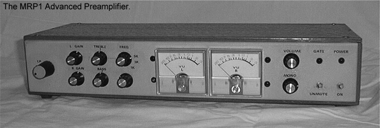
Preface Figure 1.1
The Advanced Preamplifier neatly boxed: 1976
During the development period, the need for an HF correction pole to counteract the levelling-out of the response as unity gain is approached in the first stage was appreciated; this is implemented by R1, C1 in Preface Figure 1.2. The extra 6 dB/octave roll-off exactly compensates in level and phase for the levelling-out in the first stage so long as you get its frequency right; this is not a case of an approximate bodge.
While giving excellent results considering its simplicity, the BootWalker did not have the capabilities of a discrete opamp; therefore it was not required to implement the boost in the LF region, where it might have had inadequate negative-feedback to give good linearity. The normalisation amplifier is a discrete opamp with nine transistors rather than three, and better fitted to giving high gain at low distortion. The components implementing the LF part of the RIAA were switched out of the feedback network of the normalisation amplifier when a line input was in use; all my later opamp designs do the whole of the RIAA equalisation in one stage, thanks to the Lipshitz equations. I have heard the discrete opamp approach disrespected on the grounds that ultra-low distortion occurs almost automatically; such statements show woeful ignorance, as there are many design issues to that need to be dealt with properly. These are described in [3]. Be aware that the discrete opamps used in the article here are more start-of-art than state-of-art and could be much improved in the light of today’s knowledge; for example, now I would put current mirrors in the collectors of the input pairs to enforce equality of collector current, and so prevent the generation of second-order distortion. For full details of how to make a state-of-art discrete opamp, see [3].
Absolute phase was an unheard of concept in 1976, and the phase-inversion produced here by the tone-control was ignored. It is difficult to see how it could have been fixed without adding another stage, which did nothing but invert to get the phase correct again; not exactly an economical design approach.
You may be wondering why the coupling capacitors are in most cases rather small non-electrolytics. This is because electrolytics were not as reliable then as they are now, and so I wanted to use as few as possible. Looking back, this was not my brightest idea, although I was right in the sense that the lifetime of a piece of audio equipment is still primarily limited by electrolytics drying out and falling in value. In top-end mixing consoles where internal temperatures are relatively high and 24/7 operation is the norm, the electrolytics need replacing (an extremely specialised job) long before the pots and switches are worn out.
You will note the 25 kΩ level pots and the 100 kΩ pot in the tone-control network; these values were typical of the era. In succeeding designs, I used electrolytic coupling capacitors, often of 47 uF, because this allowed the circuit impedances to be an order of magnitude lower, with corresponding reductions in Johnson noise and the effects of device input current noise. Pot impedances were reduced to 10 kΩ; for an example see Chapters 5 and 6. Since there were always electrolytic reservoir capacitors in the power supply, it seemed pointless to worry too much about a few coupling capacitors working under rather more benign conditions from the point of view of reliability.
As my thoughts on preamp design progressed, I reduced the circuit impedances in my high-end designs by another order of magnitude, so that pots were 1 kΩ, and coupling capacitors of 470 uF or 1000 uF were used whenever DC had to be blocked. The limits on this process are to an extent the increased drive requirements, though this can be easily overcome by using multiple opamps in parallel, which in itself also reduces noise by partial cancellation; see Chapters 14 and 15. A more final limit is the unavailability of two- and four-gang pots in very low values, but this too can be circumvented by using multiway switches and resistor ladders.
Let us see how far this idea can be pushed. If the pots/switched-resistor-networks are reduced to 100 Ω then driving them with paralleled opamps starts to get clumsy, as you would probably need to use eight of them for a good distortion performance. Using opamps combined with discrete output transistors may cut the component count but is likely to impact the THD for the worse. If you decide to get really radical and replace the opamps with power amplifiers, I suppose the ultimate limit would be overall power dissipation; imagine driving a 10 Ω volume control at 10 Vrms (roughly maximum opamp level). You would be dissipating 10 W in the pot, or 20 W for stereo; if you insist on a pot rather than switched-resistors, it’s going to be a wirewound rheostat (I actually have some of them in my component collection, but unfortunately none are double gang for stereo.) Good luck getting a rheostat with a log law. Admittedly 10 Vrms is a high level, and for a more likely 2 Vrms, the pot dissipation is 400 mW, and more doable, but this will be repeated at many places in the circuitry. Apart from the problems of sourcing dual-gang log rheostats, there are likely to be crosstalk and offness problems if the ground connections are not equally reduced in impedance, which won’t be easy.
Pushing the idea a little further, the use of power amplifiers removes the level limitations of opamps. With ±45 V rails, we could sustain 28 Vrms, 9 dB above 10 Vrms, which could be used to either increase headroom or signal/noise ratio (by raising the internal level), but we would then be dissipating 80 W in our 10 Ω volume control. This is obviously well beyond the line of sensible, but in hi-fi, that is a very blurred line. If you want to take the idea even further, I will merely observe that there is no difficulty in designing an amplifier to drive a 2 Ω load, and leave you to it.
If you’re wondering if this sort of thing has been tried for real, the answer is yes, sort of. I recall a microphone preamplifier with a very low impedance negative feedback network intended to reduce noise; this had to be driven by a power amplifier.
The LED biasing of current-sources (to minimise current changes with temperature) was an elegant method but, as I strongly suspected at the time, quite unnecessary, as the discrete op-amps used are really not that sensitive to their internal operating conditions. Nevertheless, as LEDs were pretty new at the time, it was generally regarded as well cool. A PCB was available from Wireless World for the princely sum of £3.50.
The level monitoring circuitry was perhaps a bit over the top, with a big pair of VU meters originally intended for a mixing desk. There were also ’1V Peak’ LEDs to indicate nominal level, and bipolar ‘Clip’ LEDs to alert the user that the ±24V rails had been hit. I have to admit that I never once saw the ‘Clip’ LEDs come on in real use. The bipolar clip-detect circuit proved extremely useful in other applications however, and I have been using it ever since. There is also a bit of an infelicity in the ‘1V Peak’ driver circuit, where the full output swing of one of the discrete op-amps is potentially applied to the trigger input of a 555 timer. Still, it never failed.
The Advanced Preamplifier was inspired by an article written by Daniel Meyer in Wireless World for July 1972. It was called: ‘Audio Pre-amplifier Using Operational Amplifier Techniques’, and still makes interesting reading, though some of the statements made are questionable. I have not been able to confirm it, but this is almost certainly the same Daniel Meyer that founded SWTP and designed the ‘Tiger’ series of power amplifiers [4].
When I measured the distortion performance of Meyer’s version of a discrete opamp in April 1975, I found the distortion performance was less than inspiring, because the output is connected directly to the VAS collector, and loading on this point is very bad for linearity; I measured 0.008% at 1 Vrms out, with a flat closed-loop gain of 16 times and ±15V supply rails (The supply rails used by Meyer). Although I was but a lad, it still seemed to me that this was rather high for what was supposed to be an advanced configuration, and I set out to improve it. In the course of this, I taught myself some of the rules of good amplifier design, such as do not connect your main gain stage directly to the load, but instead, buffer it with some kind of emitter-follower output stage. I used a constant-current emitter follower, increased the supply rails to ±30V, and voila! Less than 0.003% at 20 Vrms out. This pleasurably straightforward process started off an interest in reducing distortion which has stayed with me ever since.
A follow-up article was published called ‘Additions to the Advanced Preamplifier’ in October 1977. This added a second-order subsonic filter and a switched-frequency second-order scratch filter to the signal path. Also added was a virtual earth summing amp to give simultaneous mono and stereo outputs. (The mono output was to drive a sound-to-light converter, or light show, as we called them in those heady days.) Rather than add another complete discrete opamp, I used a simpler four-transistor circuit with the gain provided by a cascode stage using current-injection (this technique is described in the preface to Chapter 2) and a constant-current Class-A output. Other features that were described were meter suppression (to stop the VU needles smacking the end-stops at switch-on) and a remote muting facility. The latter was a switch on the end of a piece of cable rather than an IR system.
In designing these later add-ons, I was deliberately following the path of other preamp designers in Wireless World. It was definitely the done thing to come up extra features at a later date, and somehow gave the project an aura of greater import. I was danged to heck if I was going to be left out of that.
This was the first preamplifier that I developed into a completely worked-out and neatly boxed entity. The initial design work on the discrete opamps was done with the Sound Technology 1700A in 1975, using one of the first examples to enter Britain. In its day it was a major advance in audio measurement. The prototype Advanced Preamplifier was built on stripboard, but it could have been laid out as a PCB and put into production. This is therefore preamplifier No. 1 in my personal numbering system, and I described it as the MRP1. The RP naturally stands for Reference Preamplifier, and the M comes from Meadow House in Swaffham Prior, Cambridgeshire, where I was living when I did the design work.
References
1. Self, D., Small-Signal Audio Design, 2nd edition, Chapter 9, pp. 252–256. Focal Press (Taylor & Francis) 2014. ISBN: 978-0-415-70974-3 Hardback. 978-0-415-70973-6 Paperback. 978-0-315-88537-7 ebook.
2. Ibid., pp. 301–303.
3. Ibid., pp. 110–115.
4. http://en.wikipedia.org/wiki/Daniel_Meyer_(engineer) (accessed Jan. 2015)
(The Wikipedia entry claims that Meyer published an article in Electronics World in May 1960: this must refer to a USA magazine of that name as the British journal was called Wireless World at the time, and its May 1960 issue does not contain an article by Meyer.)
Advanced Preamplifier Design
November 1976
This preamplifier design offers a distortion figure of below 0.002%, an overload margin of around 47 dB, and a signal-to-noise ratio of about 71 dB for the disc amplifier. A novel noise gate mutes the output when no signal is presented to the disc input and conversely, by using the subsonic information present on record pressings, eliminates the problem of muting low-level signals.
This article describes a stereo pre-amplifier that equals or exceeds the performance of many of those available. The circuit incorporates a novel method of muting the signal path, when the disc input is quiescent, by using a noise gate that never mutes a wanted low-level signal.
Many of the important performance factors, such as signal-to-noise ratio, overload margin, and accuracy of the RIAA equalization, are essentially defined by the design of the disc input circuitry. This therefore merits close attention. The best attainable s/n ratio for a magnetic cartridge feeding a bipolar transistor stage with series feedback is about 71 dB with respect to a 2 mV r.m.s. input at 1 kHz, after RIAA equalization. This has been clearly demonstrated by Walker. [1] The equivalent amplifier stage with shunt feedback gives an inferior noise performance over most of the audio band due to the rise in cartridge source impedance with frequency. This limits the maximum s/n ratio after equalization to about 58 dB. These facts represent a limit to what the most advanced disc input stage can achieve.
Overload margin appears to be receiving little attention. The maximum velocities recorded on disc seem to be steadily increasing and this, coupled with improved cartridges, means that very high peak voltages are reaching disc inputs. Several writers have shown that short-term voltages of around 60–80 mV r.m.s. are possible from modern disc and cartridges, and higher values are to be expected. [2,3] This implies that to cater for signal maxima, a minimum overload margin of 32 dB with respect to 2 mV r.m.s. at 1 kHz is essential. Obviously a safety factor on top of this is desirable. However, most pre-amplifiers at the top end of the market provide around 35–40 dB only. There are certain honourable exceptions such as the Technics SU9600 control amplifier which achieves an overload margin of 54 dB, mainly by the use of a staggeringly high supply of 136 V in the disc input amplifier. The Cambridge P50/110 series offers a margin in excess of 60 dB by the artifice of providing unity-gain buffering, for correct cartridge loading, but no amplification before the main gain control. This allows the use of an 18 V supply rail, but does limit the maximum s/n ratio.
The overload margin of a pre-amplifier is determined by the supply voltage which sets the maximum voltage swing available, and by the amount of amplification that can be backed-off to prevent overload of subsequent stages. Most preamplifiers use a relatively high-gain disc input amplifier that raises the signal from cartridge level to the nominal operating level in one jump. Low supply voltages are normally used which reduce static dissipation and allow the use of inexpensive semiconductors. The gain control is usually placed late in the signal path to ensure low-noise output at low volume settings. Given these constraints, the overload performance is bound to be mediocre, and in medium-priced equipment the margin rarely exceeds 30 dB. If these constraints are rejected, the overload margin of the system can be improved.
Two separate gain controls remove the most difficult compromise, which is the placement of the volume control. This approach is exemplified in the Radford ZD22 and the Cambridge P60 circuitry. One gain control is placed early in the signal path, preceded by a modest amount of gain. Cartridges of high output can be accommodated by the use of this first control. The second is placed late in the pre-amplifier and is used as a conventional volume control, see Figure 1.1.

Figure 1.1
Block diagram of the complete circuit. Two gain controls are used in the signal path to allow a substantial increase in overload margin.
The other performance criterion which is largely defined by the disc input circuitry is frequency response, as defined by the accuracy of the RIAA equalization. Assuming that the relevant amplifying stage has sufficient open-loop gain to cope with the bass boost required, the accuracy of the equalization depends entirely on the time constants within the feedback loop. Careful design, and the use of close-tolerance components can assure an accurate response to within ± 0.2 dB from 30 Hz to 20 kHz.
Pre-amplifier distortion seems to have received little attention compared with that generated by power amplifiers, perhaps because the former has traditionally been much lower. However, power amplifiers, with such low THD that the residual harmonics can no longer be extracted from the noise at normal listening levels, are now commonplace, particularly with the advent of techniques such as current dumping. This desirable state of affairs unfortunately does not extend to pre-amps, which in general produce detectable distortion at nominal operating levels, usually between 0.02% and 0.2%. In this design the THD at 1 kHz is less than 0.002% even at 25 dB above the nominal operating level of 0 dBm. A Sound Technology 1700 A distortion measurement system was used during development.
At this point it is convenient to consider the noise gate principle. When the pre-amplifier is being used for disc reproduction the output from each channel is continuously sampled to determine if a signal is present; if nothing is detected within a specified time interval, dependent on the previous signal levels received, the pre-amplifier is muted by the opening of a reed relay in series with the output signal path. This allows only power amplifier noise to reach the loudspeakers and considerably reduces the perceived noise generated by a quiescent sound system. Noise in the quiescent state is particularly noticeable when headphones are in use. The reed relay is also used to prevent switch-on transients from reaching an external power amplifier. So far this circuit appears to be a fairly conventional noise gate. The crucial difference is that signals from disc that have not been subjected to rumble filtering are always accompanied by very low frequency signals generated by record ripples and small-scale warps. Even disc pressings of the highest quality produce this subsonic information, at a surprisingly high level, partly due to the RIAA bass boosting. The 1.f. component is often less than 20 dB below the total programme level but this is quite sufficient to keep the pre-amplifier unmuted for the duration of a 1.p. side. The preamplifier is unmuted as soon as the stylus touches the disc, and muted about a second after it has been raised from the run-out groove. This delay can be made short because the relative quiet at the start of the run-out groove is sensed and stored. The rumble performance of the record deck is largely irrelevant because virtually all of the subsonic information is generated by disc irregularities.
Audio circuitry
A detailed block diagram of the pre-amplifier is shown in Figure 1.1, and Figure 1.2 shows the main signal path. The disc input amplifier uses a configuration made popular by Walker, but the collector load of the second transistor is bootstrapped. This increases the open-loop gain and hence improves the closed-loop distortion performance by a factor of about three to produce less than 0.002% at an output of 6.5 V r.m.s. (1 kHz). This stage gives a s/n ratio (ref 2 mV) of about 70 dB and a gain of 15 at 1 kHz. This is sufficient to ensure that the noise performance is not degraded by subsequent stages of amplification. The maximum output of this stage before clipping is about 6.5 V r.m.s. and the nominal output is 30 mV r.m.s. Because this is the only stage before the input gain control, these two figures set the overload margin at 47 dB. To ensure that this overload margin is maintained at high frequencies, the treble-cut RIAA time-constant is incorporated in the feedback loop. This leads to slightly insufficient cut at frequencies above 10 kHz because the gain of the stage cannot fall below unity, and hence fails to maintain the required 6 dB/octave fall at the top of the audio spectrum. This is exactly compensated for outside the feedback loop by the low-pass filter R1 C1, which also helps to reject high frequencies above the audio band.
For convenience I have referred to the next stage of the circuit as the normalization amplifier because signals leaving this should be at the nominal operating level of 0 dBm by manipulation of the input gain controls. Separate controls are provided for each channel to allow stereo balance. A later ganged control is used for volume setting and causes no operational inconvenience. In the disc replay mode, the normalization amplifier provides the RIAA bass boost, by the feedback components R2+3 and C2. Two line inputs are also provided; line low requiring 30 mV and line high 100 mV to give 0 dBm from the normalization stage with the input gain control fully advanced. When these inputs are selected, the feedback networks are altered to adjust the gain and give a flat frequency response. Ultrasonic filters are incorporated to ensure stability and aid r.f. rejection. Capacitor C3 in the feedback arm

Figure 1.2
Circuit diagram of the signal path. Constant-current sources are biased from an l.e.d./resistor chain for improved thermal stability.
reduces the gain to unity at d.c. for good d.c. stability. If a fault causes the amplifier output to saturate positively the capacitor is protected by a diode which has no effect on the distortion performance.

Figure 1.3
Tape output circuit. The smallest allowable load impedance for an undistorted output is about 2.2kΩ. Line inputs of the preamplifier are suitable for playback purposes.
The circuitry of the normalization amplifier is complicated because its performance is required to be extremely high. The harmonic distortion is far below 0.002% at the maximum output of 14.5 V r.m.s. which is 25 dB above nominal operating level. This large amount of preamplifier headroom allows gross preamplifier overload before clipping. The input stage of the amplifier is a differential pair with a constant-current source for good common-mode rejection. The operating currents are optimized for good noise performance, and the output is buffered by an emitter-follower. The main voltage amplifier, Tr9 has a constant-current collector load so that high voltage gain at low distortion can be obtained. This performance is only possible if the stage has very little loading so it is buffered by the active-load emitter-follower. The various current sources are biased by a l.e.d.-resistor chain because the forward voltage drop of an l.e.d. has a negative temperature coefficient that approximates closely to that of a silicon transistor Vbe drop. Hence, this method provides exceptionally stable d.c. conditions over a very wide temperature range.
After the normalization stage the signal is applied to a tone-control circuit based on the Baxandall network. The main limitation of the Baxandall system is that the turnover frequency of the treble control is fixed. In contrast, the bass control has a turnover frequency that decreases as the control nears the flat position. This allows a small amount of boost at the low end of the audio spectrum to correct for transducer shortcomings. The equivalent adjustment at the high end of the treble spectrum is not possible because boost occurs fairly uniformly above the turnover frequency for treble control settings close to flat. In this circuit the treble turnover frequency has been given three switched values which have proved useful in practice. Switch 2 selects the capacitors that determine the turnover point. The maximum boost/cut curves are arranged to shelve gently, in line with current commercial practice, rather than to continue rising or falling outside the audio range. In addition, the coupling capacitor C4 has a significant impedance at 10 Hz so that the maximum bass boost curve not only shelves but begins to fall. Full boost gives +15 dB at 30 Hz but only +8 dB at 10 Hz. The tone control system has a maximum effect of ±14 dB at 50 Hz and ±12.5 dB at 10 kHz.
The tone-control amplifier uses the same low distortion configuration as the normalization stage, but it is used in a virtual-earth mode. The main difference is that the open-loop gain has been traded for open-loop linearity by increasing the emitter resistor of the main voltage amplifier from 1 to 10 kΩ thus increasing local feedback. Resistor R4 has been increased to 5.6 k to maintain appropriate d.c. conditions. This modification makes it much easier to compensate for stability in the unity-gain condition that occurs when treble-cut is applied.
Level detection circuitry
From the tone-control section the signal is fed to the final volume control via the muting reed-relay. Note that this arrangement allows the volume control to load the input of the external power amplifier even when the relay contacts are open, thus minimising noise. The signal level leaving the tone-control stage is comprehensively monitored by the circuitry shown in Figure 1.4. Each channel is provided with two peak-detection systems, one lights a green l.e.d. for a pre-determined period if the signal level exceeds 1 V peak, and the other lights a red l.e.d. if the tone-control stage is on the verge of clipping. Each channel is also provided with a VU meter driver circuit. Transistor Tr22 forms a simple amplifying stage which also acts as a buffer. Voltage feedback is used to ensure a low-impedance drive for the meter circuitry. The first peak detector is formed by IC1 and its associated components. When the voltage at pin 2 goes negative of its quiescent level by 1 V, the timer is triggered and the l.e.d. turns on for a defined time. The relatively heavy l.e.d. current is drawn from an unstabilized supply to avoid inducing transients into any of the stabilized supplies.
The clipping detector continuously monitors the difference in voltage between the tone-control amplifier output and both supply rails. If the instantaneous voltage approaches either rail, this information is held in a peak-storage system. Normally Tr24 and Tr25 conduct continuously but if the junction of D1 and R5 approaches the +24 V rail then Tr24 and hence Tr25 turn off. This allows C5 to charge and turn on Tr26, and Tr27 and hence the l.e.d. until the charge on C5 has been drained off through emitter-follower Tr26. If the measured voltage nears the—24 V rail, then D1 conducts to pull up the junction of R6 and R7, which once again turns off Tr25. In this way both positive and negative approaches to clipping are indicated. This comprehensive level indication does of course add significantly to the task of building and testing the preamplifier. If desired, any or all of the three sections may be omitted.

Figure 1.4
Level monitoring circuitry. Although three separate circuits are shown, these may be omitted as required.
Noise gate
The final section controls the muting reed-relay. At switch-on, the +12 V rail rises rapidly until stabilized by the zener diode. Pin 2 on IC4 is, however, briefly held low by C6, and the 555 is therefore immediately triggered to send pin 3 high. This saturates Tr28 which prevents Tr29 from turning on. At the end of the time delay, pin 3 goes low and relay driver Tr29 is no longer disabled (Figure 1.5).

Figure 1.5
Noise gate and delay switch on circuitry. The noise gate is provided with an override switch for use with line input signals. The delay switch-on overrides all of the circuitry. amplifier IC2 is repeated for a stereo system.
The noise gate uses two amplifiers with gains of about 100. These sample both channels at the output of the normalization stage and the inputs are clamped with diodes so that the normalization amplifiers may use their full voltage swing capability without damaging the 741s. Due to their high gain, under normal signal conditions the op-amp outputs move continuously between positive and negative saturation which keeps the storage capacitor C7 fully charged. In the silent passages between 1.p. tracks the 1.f. signal is not normally of sufficient amplitude to cause saturation but will usually produce at least +3 to +4 V across C7 which gives a large margin of safety against unwanted muting. To facilitate this the response of the amplifiers is deliberately extended below the audio band. When the stylus leaves the record surface and the 1.f. signals cease, C7 slowly discharges until the non-inverting input of comparator IC3 falls below the voltage set on the inverting input. At this point the 741 switches and its output goes low to cut off the base drive to Tr29, and switch off the relay. When the stylus is replaced on a record, the process takes place in reverse, the main difference being that C7 charges at once due to the low forward impedance of D2. To prevent the relay sporadically operating when the preamplifier is handling signals presented through the line inputs, an extra wafer on the source-select switch is arranged to override the rumble-sensing circuit, and provide permanent unmute. This is achieved by pulling the inverting input of comparator IC3 negative of the +15 V rail by the 10 kΩ resistor so that even when C7 is fully discharged, IC3 will not switch. In addition, S3 provides a manual override for testing and comparison purposes.

Figure 1.6
Power supply. Two regulator integrated circuits are used which should be mounted on heat sinks.
The power supply is shown in Figure 1.6. Regulators are used to provide stabilized ±24 V rails. The unregulated supply rests at about ±35 V. The signal circuitry has been designed to withstand ±35 V appearing on the supply rails, so that even in the unlikely event of both regulators failing, no further destruction will arise. Each regulator IC requires about 7 cm2 of heat sink area.
Physical layout of the preamplifier is no more critical than that of any other piece of audio equipment. In general it is wise to use a layout that places the disc input amplifier as close as possible to its input socket, and as far as possible from the mains transformer. Screened cable should be used between the disc input stage and its input socket, and between the final volume control and the output socket. The earthing requirements are straightforward and the circuit common 0 V rail is led from the input sockets through the signal path to the output volume control, and finally to the 0 V terminal of the power supply. This arrangement minimises the possibility of spurious e.m.fs arising between stages. The only problem likely to be encountered is the formation of an earth loop when the preamplifier is connected to a power amplifier. Therefore, it may be satisfactory in a permanent installation to have the preamplifier circuitry connected to mains earth only through the signal lead to the power amplifier. The preamplifier case must of course be connected to the mains earth for safety reasons. It is preferable to define the potential of the preamplifier even if the power amplifier is disconnected. In the prototype the 0 V rail was connected to the mains earth via a 22 Ω resistor which stops the formation of an earth loop and prevents the signal circuitry from taking up a potential above earth due to leakage currents etc. Testing is relatively straightforward, providing the preamplifier is constructed and checked stage by stage. Dynamic parameters such as THD are not accurately measurable without expensive test gear, but it has been found in the course of experimentation that if the d.c. conditions are correct then the various signal stages almost always show the desired a.c. performance. The non-signal circuitry should be relatively simple to fault-find. No problems should be encountered with the noise gate section which has proved to be very reliable throughout a protracted period of testing. The only preamplifier adjustment is for the VU meter calibration. This should be set to IV r.m.s. = 0VU, which is completely non-standard but very useful in terms of the dynamic range of the signal path. For normal operation the input gain controls should be set so that the meter indications do not exceed 0VU, to preserve a safety margin in the later stages. This completes the preamplifier design.
Component notes
- All unmarked diodes are 1N914 or equivalent.
- Red bias I.e.ds are TIL209 or equivalent.
- Green bias l.e.ds are TIL211 or equivalent.
- Resistors marked with an asterisk should be metal oxide types
- Tr1 to Tr6 and Tr13 to Tr15 are BCY71 Tr7,8,9,16,17,18,22,23,25,26,28 are MPS A06.
- Tr10,11,12,19,20,21,24,27 are MPS A56 Tr9 is BFX85 or equivalent.
- The muting reed relay should be a two pole make type with an 18 V coil. If a different coil voltage is used, the value of the dropper resistor should be adjusted.
- The VU meter should have a 1 mA movement.
- If an internal diode and series resistor are fitted, the external components should be omitted.
- Switch 1 (source select) is a five pole 3 way.
- Switch 2 (treble frequency) is a four pole 3 way.
References
1. Walker, H.P. ‘Low-noise Audio Amplifiers’, Wireless World, May 1972.
2. King, Gordon J. The Audio Handbook, Newnes-Butterworth, 1975.
3. Heidenstrom, P.N. ‘Amplifier Overload’, Hi-Fi News, December 1974.