
Chapter 23
Distortion in power amplifiers
Part II: the input stage (Electronics World, September 1993)
The input stage of a power amplifier only has to handle small signals compared with the output signal, and so it might be thought that its contribution to the distortion of a complete power amplifier would be negligible. This is not so.
The vast majority of amplifiers use Miller dominant-pole compensation, in which a small capacitor essentially turns the VAS stage into an integrator. This gives very dependable stability, and has many other advantages, but the downside is that as the frequency increases, the amount of current that has to be pumped in and out of the Miller capacitor increases proportionally. Therefore the error voltage across the two inputs of the differential pair, which drives this current, also increases proportionally due to the global negative feedback. The signal levels here at say 20 kHz are surprisingly large, and make it essential to consider the linearity of the input stage carefully. In practical terms this means using emitter degeneration resistors of 100Ω, and a current-mirror to phase-sum the collector currents.
SPICE simulation of the input stage was found to be very helpful, demonstrating clearly the effectiveness of emitter degeneration in linearising the voltage-current relationship. It is simple to simulate an input stage in isolation, so long as you take the precaution of providing a subsequent virtual-earth stage so the output current can be absorbed while keeping a constant voltage on the input stage output node.
The beauty of the differential pair is that it is one of the few places where the much-mentioned “cancellation of second-harmonic distortion” really does work reliably and without adjustment, thanks to the great predictability of the Vbe-Ic relationship of the bipolar transistor. To make this work, it is necessary to keep the collector currents of the two devices accurately equal, and this can be done very elegantly by a current-mirror in the collectors. This circuit element also doubles the open-loop gain of the overall amplifier, and doubles its slew-rate, so there is no doubt it is earning its keep.
The article is by no means a fully comprehensive guide to input stages. Other important issues were investigated later. These include common-mode distortion, which might be expected to cause difficulties [1] as the error signal between the two inputs is usually much smaller than the common-mode voltage on both of them. However, CM distortion only becomes a measurable problem with very low closed-loop gains (say two times) which are not customary in power amplifiers.
Another issue is the increased distortion and hum that occurs when the amplifier input is driven from a significant source impedance, say more than 200Ω. This occurs because the base currents drawn by the input transistor pair are not linear even if the amplifier output is completely distortion free [2]. This is why it is an extremely bad idea to put RC filters directly on the input, in a dimwitted attempt to stop ultrasonic interference. The R is sometimes as high as 10 kΩ, which will play merry heck with the distortion and hum performance of most amplifiers.
Simple emitter degeneration with resistors provided all the linearity required at the power levels used here, but more complex and linear input stages are also examined in the chapter. CFP input stages are a definite possibility, but the cross-quad and cascomp configurations described [3] do not give an improvement in linearity consistent, with their complexity, and the cross-quad has also a nasty habit of latching-up solid unless handled very carefully. There are several other methods of improving linearity by adding two or more transistors to extend the region over which the input stage is linear, for example the multi-tanh approach. Some of these look quite promising, but I have yet to explore them in any detail.
Up to the time of writing, the simple degenerated input pair with current-mirror has still proved adequate for all requirements. If and when output stage distortion is reduced substantially, this may no longer be the case, and there is, as usual, no room for complacency.
References
1. Self, D., Audio Power Amplifier Design, 6th edition, pp. 140–142. Focal Press 2013. ISBN 978-0-240-52613-3.
2. Ibid., pp. 142–150.
3. Ibid., pp. 135–138.
Distortion in Power Amplifiers
September 1993
The input stage of an amplifier performs the critical duty of subtracting the feedback signal from the input, to generate the error signal that drives the output. It is almost invariably a differential transconductance stage; a voltage-difference input results in a current output that is essentially insensitive to the voltage at the output port. Its design is also frequently neglected, as it is assumed that the signals involved must be small, and that its linearity can therefore be taken lightly compared with that of the voltage amplifier stage (VAS) or the output stage. This is quite wrong, for a misconceived or even mildly wayward input stage can easily dominate HF distortion performance.
The input transconductance is one of the two parameters setting HF open-loop (o/l) gain, and thus has a powerful influence on stability and transient behaviour as well as distortion. Ideally the designer should set out with some notion of how much o/l gain at 20 kHz will be safe when driving worst-case reactive loads—a precise measurement method of open-loop gain was outlined last month—and from this a suitable combination of input transconductance and dominant-pole Miller capacitance can be chosen.
Many of the performance graphs shown here are taken from a model (small-signal stages only) amplifier with a Class-A emitter-follower output, at +16 dBu on ±15 V rails. However, since the output from the input pair is in current form, the rail voltage in itself has no significant effect on the linearity of the input stage. It is the current swing at its output that is the crucial factor.
Vive la differential
The primary motivation for using a differential pair as the input stage of an amplifier is usually its low DC offset. Apart from its inherently lower offset due to the cancellation of the Vbe voltages, it has the added advantage that its standing current does not have to flow through the feedback network. However a second powerful reason is that its linearity is far superior to single-transistor input stages. Figure 23.1 shows three versions, in increasing order of sophistication. The resistor-tail version in Figure 23.1(a) has poor CMRR and PSRR and is generally a false economy; it will not be further considered. The mirrored version in Figure 23.1(c) has the best balance, as well as twice the transconductance of that in Figure 23.1(b).
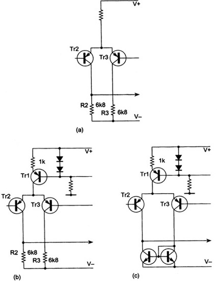
Figure 23.1
Three versions of an input pair: (a) Simple tail resistor; (b) Tail currentsource; (c) With collector current-mirror to give inherently good lc balance.
Intuitively, the input stage should generate a minimal proportion of the overall distortion because the voltage signals it handles are very small, appearing as they do upstream of the VAS that provides almost all the voltage gain. However, above the first pole frequency P1, the current required to drive Cdom dominates the proceedings, and this remorselessly doubles with each octave, thus:
For example the current required at 100 W, 8 Ω and 20 kHz, with a 100 pF Cdom is 0.5 mA peak, which may be a large proportion of the input standing current, and so the linearity of transconductance for large current excursions will be of the first importance if we want low distortion at high frequencies.
Figure 23.2, curve A, shows the distortion plot for a model amplifier (at +16 dBu output) designed so that the distortion from all other sources is negligible compared with that from the carefully balanced input stage. With a small-signal class A stage this essentially reduces to making sure that the VAS is properly linearised. Plots are shown for both 80 kHz and 500 kHz measurement bandwidths to show both HF behaviour and LF distortion. It demonstrates that the distortion is below the noise floor until 10 kHz, when it emerges and heaves upwards at a precipitous 18 dB/octave.

Figure 23.2
Distortion performance of model amplifier differential pair at A compared with singleton input at B. The singleton generates copious second-harmonic distortion.
This rapid increase is due to the input stage signal current doubling with every octave to drive Cdom; this means that the associated third harmonic distortion will quadruple with every octave increase. Simultaneously the overall NFB available to linearise this distortion is falling at 6 dB/octave since we are almost certainly above the dominant pole frequency P1. The combined effect is an 18 dB/octave rise. If the VAS or the output stage were generating distortion, this would be rising at only 6 dB/octave and would look quite different on the plot.
This form of non-linearity, which depends on the rate-of-change of the output voltage, is the nearest thing to what we normally call TID, an acronym that now seems to be falling out of fashion. Slew-induced-distortion SID is a better description of the effect.
If the input pair is not accurately balanced, then the situation is more complex. Second as well as third harmonic distortion is now generated, and by the same reasoning this has a slope of closer to 12 dB/octave. This vital point requires examination.
Input stage in isolation
The use of a single input transistor (Figure 23.3(a)) sometimes seems attractive, where the amplifier is capacitor-coupled or has a separate DC servo; it at least promises strict economy. However, the snag is that this singleton configuration has no way to cancel the second-harmonics generated by its strongly-curved exponential Vin / Iout characteristic. [1] The result is shown in Figure 23.2 curve B, where the distortion is much higher, though rising at the slower rate of 12 dB/octave.
Although the slope of the distortion plot for the whole amplifier tells much, measurement of input-stage nonlinearity in isolation tells more. This may be done with the test circuit of Figure 23.4. The op-amp uses shunt feedback to generate an appropriate AC virtual earth at the input-pair output. Note that this current-to-voltage conversion op-amp requires a third −30 V rail to allow the i/p pair collectors to work at a realistic DC voltage—i.e. about one diode’s-worth above the −15 V rail. Rf can be scaled to stop op-amp clipping without effect to the input stage. The DC balance of the pair may be manipulated by VR1: it is instructive to see the THD residual diminish as balance is approached until, at its minimum amplitude, it is almost pure third harmonic.
The differential pair has the great advantage that its transfer characteristic is mathematically highly predictable. [2] The output current is related to the differential input voltage Vin by:
where Vt is the usual ‘thermal voltage’ of about 26 mV at 25 °C and Ie the tail current.
This equation demonstrates that the transconductance, gm, is highest at V in = 0 when the two collector currents are equal, and that that the value of this maximum is proportional to the tail current, Ie. Note also that beta does not figure in the equation, and that the performance of the input pair is not significantly affected by transistor type.
Figure 23.5(a) shows the linearising effect of local feedback or degeneration on the voltage-in/current-out law. Figure 23.5(b) plots transconductance against input
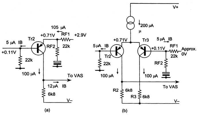
Figure 23.3
Singleton and differential pair input stages showing typical DC conditions. The large DC offset of the singleton(2.8 V) is largely due to all the stage current flowing through the feedback resistor RF1.
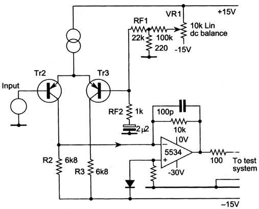
Figure 23.4
Test circuit for examining input stage distortion in isolation. The shunt-feedback opamp is biased to provide the right DC conditions for Tr2.

Figure 23.5
Effect of degeneration on input pair V/l law, showing how transconductance is sacrificed in favour of linearity (SPICE simulation).
voltage and demonstrates a reduced peak transconductance value but with the curve made flatter and more linear over a wider operating range. Adding emitter degeneration markedly improves input stage linearity at the expense of noise performance. Overall amplifier feedback factor is also reduced since the HF closed-loop gain is determined solely by the input transconductance and the value of the dominant-pole capacitor.
Input stage balance
One relatively unknown property of the differential pair in power amplifiers is its sensitivity to exact DC balance. Minor deviations from equality of Ic in the pair seriously upset the second-harmonic cancellation by moving the operating point from A in Figure 23.5(a) to B. Since the average slope of the characteristic is greatest at A, serious imbalance also reduces the open-loop gain. The effect of small amounts of imbalance is shown in Figure 23.6 and Table 23.1: for an input of −45 dBu a collector current imbalance of only 2% increases THD from0.10% to 0.16%; for 10% imbalance this deteriorates to0.55%. Unsurprisingly, imbalance in the other direction (Ic1 > I c2) gives similar results.
This gives insight [4] into the complex changes that accompany the simple changing the value of R2. For example, we might design an input stage as per Figure 23.7(a), where R1 has been selected as 1 kΩ by uninspired guesswork and R2 made highish at 10 kΩ in a plausible but misguided attempt to maximise o/l gain by minimising loading on Tr 1 collector. R3 is also made 10 kΩ to give the stage a notional ‘balance’, though unhappily this is a visual rather than electrical balance. The asymmetry is shown in the resulting collector currents: this design will generate avoidable second harmonic distortion, displayed in the 10 kΩ curve of Figure 23.8.
However, recognising the importance of DC balancing, the circuit can be rethought as per Figure 23.7(b). If the collector currents are to be roughly balanced, then R2 must be about 2 × R1, as both have about 0.6 V across them. The effect of this change is shown in the 2.2 kΩ curve of Figure 23.8. The improvement is accentuated as the o/l gain has also increased by some 7 dB, though this has only a minor effect on the closed-loop linearity compared with the improved balance of the input pair. R3 has been excised as it contributes little to stage balance.
The joy of current mirrors
While the input pair can be approximately balanced by the correct choice of R1 and R2, other circuit tolerances are significant and Figure 23.6 shows that balance is critical, needing to be accurate to at least 1% for optimal linearity. The standard current-mirror configuration
Figure 23.6
Effect of collector-current imbalance on an isolated input pair; the second harmonic rises well above the level of the third if the pair moves away from balance by as little as 2%.
Table 23.1 Key to Figure 23.6
| Curve No. | IcImbalance (%) |
|
|
|
| 1 | 0 |
| 2 | 0.5 |
| 3 | 2.2 |
| 4 | 3.6 |
| 5 | 5.4 |
| 6 | 6.9 |
| 7 | 8.5 |
| 8 | 10 |
Imbalance defined as deviation of Ic (per device) from that value which gives equal currents in the pair.

Figure 23.7
Improvements to the input pair: (a) Poorly designed version; (b) Better … partial balance by correct choice of R2.(c) Best … near-perfect Ic balance enforced by mirror.

Figure 23.8
Distortion of model amplifier: (a) Unbalanced with R2 = 10 kΩ; (b) Partially balanced with R = 2.2 kΩ; (c) Accurately balanced by current-mirror.
shown in Figure 23.7(c) forces the two collector currents very close to equality, giving proper cancellation of second harmonic. The resulting improvement shows up in the current-mirror curve of Figure 23.8. There is also less DC offset due to unequal base currents flowing through input and feedback resistances; we often find that a power-amplifier improvement gives at least two separate benefits. This simple mirror has its own residual base current errors but they are not large enough to affect distortion.
The hyperbolic tangent law also holds for the mirrored pair, [3] though the output current swing is twice as great for the same input voltage as the resistor-loaded version. This doubled output occurs at the same distortion level as for the single-ended version, as linearity depends on the input voltage, which has not changed. Alternatively, to get the same output we can halve the input which, with a properly balanced pair generating only third harmonic, will produce just one-quarter the distortion, a pleasing result.
A low cost mirror made from discrete transistors forgoes the Vbe matching available to IC designers, and so requires its own emitter degeneration for good current-matching. A voltage drop across the mirror emitter resistors in the range 30–60 mV will be enough to make the effect of V be tolerances on distortion negligible If degeneration is omitted, there is significant variation in HF distortion performance with different specimens of the same transistor type. Adding a current mirror to a reasonably well balanced input stage will increase the total o/l gain by at least 6 dB, and by up to 15 dB if the stage was previously poorly balanced. This needs to be taken into account in setting the compensation. Another happy consequence is that the slew-rate will be roughly doubled, as the input stage can now source and sink current into Cdom without wasting it in a collector load. If Cdom is 100 pF, the slewrate of Figure 23.7(b) is about 2.8 V/μs up and down, while Figure 23.7(c) gives5.6 V/μs. The unbalanced pair in Figure 23.7(a) displays further vices by giving 0.7 V/μs positive-going and 5 V/μs negative-going.
Improving linearity
Now that the input pair has been fitted with a mirror, we may still feel that the HF distortion needs further reduction; after all, once it emerges from the noise floor it goes up eight times with each doubling of frequency, and so it is well worth pushing the turn point as far as possible up the frequency range. The input pair shown has a conventional value of tail-current. We have seen that the stage transconductance increases with I c, and so it is possible to increase the gm by increasing the tail-current, and then return it to its previous value (otherwise C dom would have to be increased proportionately to maintain stability margins) by applying local NFB in the form of emitter-degeneration resistors. This ruse powerfully improves input linearity despite its rather unsettling flavour of something-for-nothing. The transistor nonlinearity can here be regarded as an internal nonlinear emitter resistance re, and what we have done is to reduce the value of this (by increasing Ic) and replace the missing part of it with a linear external resistor, Re.
For a single device, the value of re can be approximated by:
Our original stage at Figure 23.9(a) has a perdevice Ic of 600 μA, giving a differential (i.e. mirrored) gm of 23 mA/V and re = 41.6 Ω. The improved version at Figure 23.9(b) has I c = 1.35 mA and so re = 18.6 Ω. Emitter degeneration resistors of 22 Ω are required to reduce the gm back to its original value, as 18.6 + 22 = 41.6. The distortion measured by the circuit of Figure 23.4 for a −40 dBu input voltage is reduced from 0.32% to0.032%, which is an extremely valuable linearisation, and will translate into a distortion reduction at HF of about five times for a complete amplifier. For reasons that will emerge later the full advantage is rarely gained. The distortion remains a visually pure third harmonic so long as the input pair remains balanced. Clearly this sort of thing can only be pushed so far, as the reciprocal-law reduction of re is limited by practical values of tail current. A name for this technique seems to be lacking; ‘constant- gm degeneration’ is descriptive but rather a mouthful.
Since the standing current is roughly doubled so has the slew rate: 10 V/μs to 20 V/μs. Once again we gain two benefits for the price of one modification.
For still better linearity, various techniques exist. When circuit linearity needs a lift, it is often a good approach to increase the local feedback factor, because if this operates in a tight local NFB loop there is often little effect on the overall global-loop stability. A reliable method is to replace the input transistors with complementary-feedback (CFP or Sziklai) pairs, as shown in the stage of Figure 23.10(a). If an isolated input stage is measured using the test circuit of Figure 23.4, the constant gm degenerated version shown in Figure 23.9(b) yields 0.35% third-harmonic distortion for a −30 dBu input voltage, while the CFP version gives 0.045%. Note that the input level here is 10 dB up on the previous example to get well clear of the noise floor. When this stage is put to work in a model amplifier, the third-harmonic distortion at a given frequency is roughly halved, assuming other distortion sources have been appropriately minimised. However, given the steep slope of input stage

Figure 23.9
Input pairs before and after constant-gm degeneration showing how to double stage current while keeping transconductance constant: distortion is reduced by about ten times.
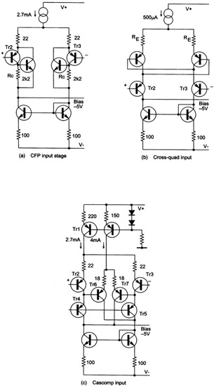
Figure 23.10
Some enhanced differential pairs: (a) The complementary feedback pair; (b) The cross-quad; (c) The cascomp.

Figure 23.11
Whole-amplifier THD with normal and CFP input stages; input stage distortion only shows above noise floor at 20 kHz, so improvement occurs above this frequency. The noise floor appears high as the measurement bandwidth is 500 kHz.
distortion, this extends the low distortion regime up in frequency by less than an octave. See Figure 23.11.
The CFP circuit does require a compromise on the value of Rc, which sets the proportion of the standing current that goes through the NPN and PNP devices on each side of the stage. In general, a higher value of Rc gives better linearity, but more noise, due to the lower Ic in the NPN devices that are the inputs of the input stage, as it were, causing them to match less well the relatively low source resistances. 2.2 kΩ is a reasonable compromise.
Other elaborations of the basic input pair are possible. Power amp design can live with a restricted common-mode range in the input stage that would be unusable in an op-amp, and this gives the designer great scope. Complexity in itself is not a serious disadvantage as the small-signal stages of the typical amplifier are of almost negligible cost compared with mains transformers, heat-sinks, etc.
Two established methods to produce a linear input transconductance stage (often referred to in opamp literature simply as a transconductor) are the cross-quad [5] and the cascomp [6] configurations. The cross-quad (Figure 23.10(b)) gives a useful reduction in input distortion when operated in isolation but is hard to incorporate in a practical amplifier because it relies on very low source resistance to tame the negative conductances inherent in its operation. The cross-quad works by imposing the input voltage to each half across two base-emitter junctions in series, one in each arm of the circuit. In theory the errors due to non-linear re of the transistors is divided by beta, but in practice things seem less rosy.
The cascomp (Figure 23.10(c)) does not have this snag, though it is significantly more complex to design. Tr2, Tr3 are the main input pair as before, delivering current through cascode transistors Tr 4, Tr5 (this does not in itself affect linearity) which, since they carry almost the same current as Tr2, Tr3 duplicate the input Vbev errors at their emitters. This is sensed by error diff-amp Tr 6, Tr7 whose output currents are summed with the main output in the correct phase for error-correction. By careful optimisation of the (many) circuit variables, distortion at −30 dBu input can be reduced to about 0.016% with the circuit values shown. Sadly, this effort provides very little further improvement in whole-amplifier HF distortion over the simpler CFP input, as other distortion mechanisms are coming into play—for instance the finite ability of the VAS to source current into the other end of Cdom.
Power amplifiers with pretensions to sophistication sometimes add cascoding to the standard input differential amplifier. This does nothing to improve input stage linearity as there is no appreciable voltage swing on the input collectors; its main advantage is reduction of the high Vce that the input devices work at. This allows cooler running, and therefore possibly improved thermal balance; a V ce of 5 V usually works well. Isolating the input collector capacitance from the VAS input often allows Cdom to be somewhat reduced for the same stability margins, but it is doubtful if the advantages really outweigh the increased complexity.
Other considerations
As might be expected, the noise performance of a power amplifier is set by the input stage, and so it is briefly examined here. Power amp noise is not an irrelevance: a powerful amplifier is bound to have a reasonably high voltage gain and this can easily result in a faint but irritating hiss from efficient loudspeakers even when the volume control is fully retarded. In the design being evolved here the EIN has been measured at −120 dBu, which is only 7 or 8 dB inferior to a first-class microphone preamplifier. The inferiority is largely due to the source resistances seen by the input devices being higher than the usual 150 Ω microphone impedance. For example, halving the impedance of the feedback network shown in ptl (22 kΩ and 1 kΩ) reduces the EIN by approx 2 dB.
Slew rate is another parameter usually set by the input stage, and has a close association with HF distortion. The amplifier slew rate is proportional to the input’s maximum-current capability, most circuit configurations being limited to switching the whole of the tail current to one side or the other. The usual differential pair can only manage half of this, as with the output slewing negatively half the tail-current is wasted in the input collector load R2. The addition of an input current-mirror, as advocated, will double the slew rate in both directions. With a tail current of 1.2 mA, the slew rate is improved from about 5 V/μs to 10 V/μs. (for Cdom = 100 pF) The constant gm degeneration method of linearity enhancement in Figure 23.9 further increases it to 20 V/μs. The mathematics of voltage-slewing is simple:
Slew rate = I/C dom in V/μs for maximum I in μΑ, Cdom in pF.
The maximum output frequency for a given slew rate and voltage is:
Likewise, a sinewave of given amplitude has a maximum slew-rate (at zero-crossing) of:
So, for example, with a slew rate of 20 V/μs the maximum frequency at which 35 V r.m.s. can be sustained is 64 kHz, and if Cdom is 100 pF, then the input stage must be able to source and sink 2 mA peak.
A vital point is that the current flowing through Cdom must be sourced/sunk by the VAS as well as the input pair. Sinking is usually no problem, as the VAS common-emitter transistor can be turned on as hard as required. The current source or bootstrap at the VAS collector will however have a limited sourcing ability, and this can often turn out to be an unexpected limitation on the positive-going slew rate.
References
1. Gray and Meyer, Analysis & Design of Analog Integrated Circuits, Wiley 1984, p 172 (exponential law of singleton).
2. Gray and Meyer, Analysis and Design of Analog Integrated Circuits, p 194 (tanh law of simple pair).
3. Gray and Meyer, Analysis and Design of Analog Integrated Circuits, p 256 (tanh law of current-mirror pair).
4. Self, Sound Mosfet Design Electronics & Wireless World, September 1990.
5. Feucht, Handbook of Analog Circuit Design, Academic Press 1990, p 432.
6. Quinn, IEEE International Solid-State Circuits Conference, THPM 14.5, p 188 (Cascomp).