The operational amplifier is the basic building block for analog circuits, and progress in op-amp performance is the “litmus test” for linear IC technology in much the same way as progress in memory devices is for digital technology. This chapter will be devoted to op-amps and comparators, with a tailpiece on voltage references. Volumes have already been written about op-amp theory and circuit design, and these aspects will not be repeated here. Rather, we shall take a look at the departures from the ideal op-amp parameters that are found in practical devices and survey the trade-offs—including cost and availability, as well as technical factors—that have to be made in real designs. Some instances of anomalous behavior will also be examined.
The operational amplifier is the basic building block for analog circuits, and progress in op-amp performance is the “litmus test” for linear IC technology in much the same way as progress in memory devices is for digital technology. This chapter will be devoted to op-amps and comparators, with a tailpiece on voltage references. This is not to deny the enormous and ever-widening range of other analog functions that are available, but these are intended for specific niche applications, and little can be generalized about them.
Volumes have already been written about op-amp theory and circuit design and these aspects will not be repeated here. Rather, we shall take a look at the departures from the ideal op-amp parameters that are found in practical devices and survey the trade-offs—including cost and availability, as well as technical factors—that have to be made in real designs. Some instances of anomalous behavior will also be examined.
5.1. The Ideal Op-Amp
The following set of characteristics (in no particular order, since they are all unattainable) defines the ideal voltage gain block:
• infinite input impedance, no bias current
• zero output impedance
• arbitrarily large input and output voltage range
• arbitrarily small supply current and/or voltage
• infinite operating bandwidth
• infinite open-loop gain
• zero input offset voltage and current
• zero noise contribution
• absolute insensitivity to temperature, power rail, and common-mode input fluctuations
• zero cost
• off-the-shelf availability in any package
• compatibility between different manufacturers
• perfect reliability
Since none of these features is achievable, you have to select a practical op-amp from the multitude of imperfect types on the market to suit a given application. Some basic examples of trade-offs are as follows:
• A high-frequency ac amplifier will need maximum gain-bandwidth product (GBW) but will not be interested in bias current or offset voltage.
Table 5.1
Parameters for Applications Categories
Category
GBW MHz
Slew Rate
V/μs
VOS
mV
ICC
mA
VOS Drift μV/°C
Noise nV/√Hz
Gain/Phase
Error%
General purpose
1–30
0.5–40
0.5–20
Low power
0.05–5
0.03–3
0.5–20
0.015–1
Precision
0.3–10
0.06–0.5
0.5–4
3–30
High speed and video
30–1000
100–5000
1–25
3–15
0.01–0.3
• A battery-powered circuit will want the best of all the parameters but at minimum supply current and voltage.
• A consumer design will need to minimize the cost at the expense of technical performance.
• A precision instrumentation amplifier will need minimum input offsets and noise but can sacrifice speed and cheapness.
Device data sheets contain some but not all of the necessary information to make these trade-offs (most crucially, they say nothing about cost and availability, which you must get from the distributor). The functional characteristics often need some interpretation and critical parameters can be hidden or even absent. In general, if a particular parameter you are interested in is not given in the data sheet, it is safest to assume a pessimistic figure. It means that the manufacturer is not prepared to test his devices for that parameter or to certify a minimum or maximum value.
5.1.1. Applications Categories
In fact, although there is a bewildering variety of devices available, op-amps are divided into a few broad categories based on their application, in which the above trade-offs are altered in different directions. Table 5.1 suggests a reasonable range over which you might expect to find a spread of certain critical parameters for op-amps in each category.
5.2. The Practical Op-Amp
5.2.1. Offset Voltage
Input offset voltage VOS can be defined as that differential dc voltage required between the inverting and noninverting inputs of an amplifier to drive its output to zero. In the perfect amplifier, 0V in will give 0V out; practical devices will show offsets ranging from tens of millivolts down to a few microvolts. The offset appears as an error voltage in series with the actual input voltage. Definitions vary, but a “precision” op-amp is usually considered to be one that has a VOS of less than 200μV and a VOS temperature coefficient (see later) of less than 2μV/°C. Bipolar input op-amps are the best for very low–offset voltage applications unless you are prepared to limit the bandwidth to a few tens of hertz, in which case the CMOS chopper-stabilized types come into their own. The chopper technique achieves very low values of VOS and drift by repeatedly nulling the amplifier's actual VOS several hundred times a second with the aid of charge storage capacitors.
Offset voltage errors are usually quoted with reference to the amplifier circuit input. The output offset voltage is the input offset times the closed-loop gain. This can have embarrassing consequences particularly in high-gain ac amplifiers where the designer has neglected offset errors because, for performance purposes, they are unimportant. Consider a noninverting ac-coupled amplifier with a gain of 1000 as depicted in Fig. 5.1.
Let us say the circuit is for audio applications and the op-amp is one half of a TL072 selected for low noise and wide bandwidth, running on supply voltages of ±12V. The TL072 has a maximum quoted VOS of 10mV. In the circuit shown, this will be amplified by the closed-loop gain to give a dc offset at the output of 10V—which is far too close to the supply rail to leave any headroom to cope with overloads. In fact, the TL072 is likely to saturate at 9–10V anyway with ±12-V power rails.
Output Saturation Due to Amplified Offset
The designer may be wanting 2mV pk–pk ac signals at the input to be amplified up to 2-V pk–pk signals at the output. If the dc conditions are taken for granted then you might expect at least 20dB of headroom: ±1V output swing with ±10V available. But, with a worst-case VOS device virtually no headroom will be available for one polarity of input and 20V will be available for the other. Unipolar (asymmetrical) clipping will result. The worst outcome is if the design is checked on the bench with a device, which has a much-better-than-worst-case offset, say 1mV. Then the dc output voltage will only be 1V, and virtually all the expected headroom will be available. If this design is let through to production then the scene is set for unexpected customer complaints of distortion! An additional problem presents itself if the output coupling capacitor is polarized: the dc output voltage can assume either polarity depending on the polarity of the offset. If this is not recognized it can lead to early failure of the capacitor in some production units.
Figure 5.1 Noninverting AC Amplifier and the Problem of Headroom.
Reducing the Effect of Offset
The solutions are plentiful. The easiest is to change the feedback to ac coupling, which gives a dc gain of unity so that the output dc voltage offset is the same as the input offset (Fig. 5.2). The inverting configuration is simpler in this respect. The difficulty with this solution is that the time constant Rf×C can be inordinately long, leading to power-on delays of several seconds.
The second solution is to reduce the gain to a sensible value and cascade gain blocks. For instance, two ac-coupled gain blocks with a gain of 33 each, cascaded, would have the same performance but the offsets would be easily manageable. The bandwidth would also be improved, along with the out-of-band roll-off, if this were necessary. Unfortunately, this solution adds components and therefore cost.
A third solution is to use an amplifier with a better VOS specification. This will either involve a trade-off in gain bandwidth, power consumption or other parameters, or cost. For instance, in the above example, AD's OP-227G with a maximum offset of 180μV might be a suitable candidate, though it is noticeably more expensive. The overall cost might work out the same though, given the reduction in components over the second solution.
Figure 5.2 AC Coupling to Reduce Offset.
Offset Drift
Offset voltage drift is closely related to initial offset voltage and is a measure of how VOS changes with temperature and time. Most manufacturers will specify drift with temperature, but only those offering precision devices will specify drift over time. Present technology for standard devices allows temperature coefficients of between 5 and 40μV/°C, with 10μV/°C being typical. For bipolar inputs, the magnitude of drift is directly related to the initial offset at room temperature. A rule of thumb is 3.3μV/°C for each millivolt of initial offset. This drift has to be added to the worst-case offset voltage when calculating offset effects and can be significant when operating over a wide temperature range.
Early MOS-input op-amps suffered from poor offset voltage performance due to gate threshold voltage shifts with time, temperature, and applied gate voltage. New processes, particularly developments in silicon gate technology, have overcome these problems and CMOS op-amps (Texas Instruments' LinCMOS range for instance) can achieve bipolar-level VOS figures with extremely good drift, 1−2μV/°C being quoted.
Circuit Techniques to Remove the Effect of Drift
Microprocessor control has allowed new analog techniques to be developed and one of these is the nulling of input amplifier offsets, as in Fig. 5.3. With this technique the initial circuit offsets can be calibrated out of the system by applying a zero input, storing the resultant input value (which is the sum of the offsets) in nonvolatile memory and subsequently subtracting this from real-time input values. With this technique, only offset drifts, not absolute offset values, are important. Alternatively, for the cost of a few extra components—analog switches and interfacing—the nulling can be done repetitively in real time, and even the drift can be subtracted out. (This is the microprocessor equivalent of the chopper op-amps discussed earlier.)
Figure 5.3 Offset Nulling With a Microcontroller.
5.2.2. Bias and Offset Currents
Input bias current is the average dc current required by the inputs of the amplifier to establish correct bias conditions in the first stage. Input offset current is the difference in the bias current requirements of the two input terminals. A bipolar input stage requires a bias current, which is directly related to the current flowing in the collector circuit, divided by the transistor gain. FET-input (or biFET) op-amps on the other hand do not require a bias current as such, and their input currents are determined only by leakage and the need for input protection.
Bias Current Levels
Input bias currents of bipolar devices range from a few microamps down to a few nanoamps, with most industry-standard devices offering better than 0.5μA. There is a well-established trade-off between bias current and speed; high speeds require higher first-stage collector currents to charge the internal node capacitance faster, which in turn requires higher bias currents. Precision bipolar op-amps achieve less than 20nA while some devices using current nulling techniques can boast picoamp levels. Junction field-effect transistor (JFET) and CMOS devices routinely achieve input currents of a few picoamps or tens of picoamps at 25°C, but because this is almost entirely reverse-bias junction leakage it increases exponentially with temperature (see Section 4.1.3). Industry-standard JFET op-amps are therefore no better than bipolar ones at high temperatures, though precision JFET and CMOS still show nanoamp levels at the 125°C extreme. Note that even the 25°C figure for JFETs can be misleading, because it is quoted at 25°C junction temperature: many JFET op-amps take a fairly high supply current and warm up significantly in operation, so that the junction temperature is actually several degrees or tens of degrees higher than ambient.
The significance of input bias and offset currents is twofold: they determine the steady-state input impedance of the amplifier, and they result in added voltage offsets. Input impedance is rarely quoted as a parameter on op-amp data sheets since bias currents are a better measure of actual effects. It is irrelevant for the closed-loop inverting configuration, since the actual impedance seen at the op-amp input terminals is reduced to near zero by feedback. The input impedance of the noninverting configuration is determined by the change in input voltage divided by the change in bias current due to it.
Output Offsets Due to Bias and Offset Currents
Of more importance is the bias current's contribution to offsets. The bias current flowing in the source resistance RS at each terminal generates a voltage in series with the input; if the bias currents and source resistances were equal, the voltages would cancel out and no extra offset would be added (Fig. 5.4).
Figure 5.4 Bias and Offset Currents.
Ideal situation: IB, RS equal at + and − terminals, so VS+=VS−=IB×RS and ΔVOS=0
Bad design: RS not equal at + and − terminals so, neglecting IOS, VS+=IB×R3, VS−=IB×R1//R2 and ΔVOS=IB×(R1//R2−R3)
Practical op-amp: IB− differs from IB+ by IOS, RS equal at both terminals, so VS+=IB+×RS, VS−=(IB+IOS)×RS and ΔVOS=IOS×RS
As it is, the offset current generates an effective offset voltage given by IOS×RS (with a temperature coefficient determined by both), which adds to, or subtracts from, the inherent offset voltage VOS of the op-amp. Clearly, whichever dominates the output depends on the magnitude of RS. Higher values demand an op-amp with lower bias and offset currents. For instance, the current and voltage offsets generated by a 741's input circuit are equal when RS=33KΩ (typical VOS=1mV, IOS=30nA). The same value for the TL081 JFET op-amp is 1000MΩ (VOS=5mV, IOS=5pA).
IB itself does not contribute to offset provided that the source resistances are equal at each terminal. If they are not then the offset contribution is IB×ΔRS. Since IB can be an order of magnitude higher than IOS for bipolar op-amps, it pays to equalize RS: this is the function of R3 in the circuit above. R3 can be omitted or changed in value if current offset is not calculated to be a problem. Apart from the disadvantage of an extra component, R3 is also an extra source of noise (generated by the noise component of IB), which can weigh heavily against it in low-noise circuits.
5.2.3. Common-Mode Effects
Two factors, which because they do not appear in op-amp circuit theory can be overlooked until late in the design, are common-mode rejection ratio (CMRR) and power supply rejection ratio (PSRR). Fig. 5.5 shows these schematically. Related to these is common-mode input voltage range.
Figure 5.5 Common-Mode Power and Supply Rejection Ratio.
Common-Mode Rejection Ratio
An ideal op-amp will not produce an output when both inputs, ignoring offsets, are at the same (common mode) potential throughout the input range. In practice, gain differences between the two inputs, and variations in offset with common-mode voltage, combine to produce an error at the output as the common-mode voltage varies. This error is referred to the input (that is, divided by the gain) to produce an equivalent input common-mode error voltage. The ratio of this voltage to the actual common-mode input voltage is the CMRR, usually expressed in decibels. For example, a CMRR of 80dB would give an equivalent input voltage error of 100μV for every 1V change at both + and − inputs together. The inverting amplifier configuration is inherently immune to common-mode errors since the inputs stay at a constant level, whereas the noninverting and differential circuits are susceptible.
CMRR is not necessarily a constant. It will vary with common-mode input level and temperature, and always worsens with increasing frequency. Individual manufacturers may specify an average or a worst-case value and will always specify it at dc.
Power Supply Rejection Ratio
PSRR is similar to CMRR but relates to error voltages referred to the input as a result of changes in the power rail voltages. As before, a PSRR of 80dB with a rail voltage change of 1V would result in an equivalent input error of 100μV. Again, PSRR worsens with increasing frequency and may be only 20–30dB in the tens-to-hundreds of kilohertz range, so that high-frequency noise on the power rails is easily reflected on the output. There may also be a difference of several tens of decibels between the PSRRs of the positive and negative supply rails, due to the difference in internal biasing arrangements. For this reason, it is unwise to expect equal but antiphase power rail signals, such as mains frequency ripple, to cancel each other out.
5.2.4. Input Voltage Range
Common-mode input voltage range is usually defined as the range of input voltages over which the quoted CMRR is met. Errors quickly increase as it is exceeded. The input range may or may not include the negative supply rail, depending on the type of input. The popular LM324 range and its derivatives have a pnp emitter–coupled pair at the input, which allows operation down to slightly below the negative rail. The CMOS-input devices from Texas, National, STM, and Intersil also allow operation down to the negative rail. Some of these op-amps stop a few volts short of the positive rail, as they are optimized for operation from a single positive supply, but there are also some devices available that include both rails within their input range, known unsurprisingly as “rail-to-rail” input op-amps. Conventional bipolar devices of the 741 type, designed for ±15V rails, cannot swing to within less than 2V of each rail, and biFET types are even more restricted.
Absolute Maximum Input
The common-mode operating input voltage is normally different from the absolute maximum input voltage range, which is usually equal to the supply voltage. If you exceed the maximum input voltage without current limiting then you are likely to destroy the device; this can quite easily happen inadvertently, apart from circuits connected to external inputs, if for instance a large-value capacitor is discharged directly through the input. Even if current is limited to a safe value, overvoltages on the input can lead to unpredictable behavior. Latch-up, where the IC locks itself into a quasistable state and may draw large currents from the power supply, leading to burnout, is one possibility. Another is that the sign of the inputs may change, so that the inverting input suddenly becomes noninverting. (This was a well-known fault on early devices such as the 709.) These problems most frequently arise with capacitive coupling direct to one or other input, or when power rails to different parts of the circuit are turned on or off at different times. The safe way to guard against them is to include a reasonable amount of resistance at each input, directly in series with the input pin.
5.2.5. Output Parameters
Two factors constrain the output voltage available from an op-amp: the power rail voltage and the load impedance.
Power Rail Voltage
It should be obvious that the output cannot swing to a greater value than either power rail. Unfortunately it is often easy to overlook this fact, particularly as the power connections are frequently omitted from circuit diagrams, and with different quad op-amp packages being supplied from different rails it is hard to keep track of which device is powered from what voltage. More seriously, with unregulated supplies the actual voltage may be noticeably less than the nominal. The required output must be calculated for the worst-case supply voltage.
Historically, most op-amps could not swing their output right up to either supply rail. The profusion of CMOS-output devices have dealt with this limitation, as have many of the types intended for single-supply operation, which have a current sink at the output and can reach within a few tens of millivolts of the negative (or ground) supply terminal. Other conventional bipolar and biFET parts cannot swing to within less than 2V of either rail. The classic output stage (Fig. 5.6) is a complementary emitter follower pair, which gives low output impedance, but the output available in either direction is limited by (VDR(min)+VBE). Depending on the detailed design of the output, the swing may or may not be symmetrical in either polarity. This fact is disguised in some data sheets where the maximum peak-to-peak output voltage swing is quoted, rather than the maximum output voltage relative to the supply terminals.
Load Impedance
Output also depends on the circuit load impedance. This may again seem obvious, but there is an erroneous belief that because feedback reduces the output impedance of an op-amp in proportion to the ratio of open- to closed-loop gains, it should be capable of driving very low–load resistors. Well, of course, to an extent it is, but Ohm's law is not so easily flouted, and a low output resistance can only be driven to a low output voltage swing, depending entirely on the current drive capability of the output stage. The maximum output current that can be obtained from most devices is limited by package dissipation considerations to about ±10mA. In some cases, the output current spec is given as a particular output voltage swing when driving a stated value of load, typically 2–10kΩ. The “rail-to-rail” op-amps with CMOS output will in fact only give a full rail-to-rail swing if they are driven into an open circuit; any output load, including, of course, the feedback resistor, reduces the total available swing in proportion to the ratio of output resistance to load resistance (Fig. 5.7).
Figure 5.6 Output Voltage Swing Restrictions.
If you want more output current it is quite to buffer the output with an external complementary emitter follower or something similar, provided that feedback is taken from the final output. Take care with short-circuit protection when doing this (or else do not be surprised if you have to keep replacing transistors), and also bear in mind that you have changed the high-frequency response of the combination and the closed-loop circuit may now be unstable.
Some single-supply op-amps are not designed both to source and sink current and, when used with split supplies, may have some crossover distortion as the output signal passes through the mid-supply value.
Output current protection is universally provided in op-amps to prevent damage when driving a short circuit. This does not work in the reverse direction, that is, when the output voltage is forced outside either supply rail by a fault condition. In this case, there will be one or two forward-biased diode junctions to the power rail, and current will flow through these limited only by the fault source impedance. Preventative measures for circuits where this is likely are dealt with in Section 6.2.3.
Figure 5.7 Limits on Rail-to-Rail Swing With CMOS Outputs.
5.2.6. AC Parameters
The performance of an op-amp at high frequency is described by a motley collection of parameters, each of which refers to slightly different operating conditions. They are as follows:
• large-signal bandwidth, or full-power response: the maximum frequency, at unity closed-loop gain, for which a sinusoidal input signal will produce full output at rated load without exceeding a given distortion level. This bandwidth figure is normally determined by the slew-rate performance.
• small-signal or unity-gain bandwidth, or GBW: the frequency at which the open-loop gain falls to unity (0dB). The “small-signal” label means that the output voltage swing is small enough that slew-rate limitations do not apply.
• slew rate: the maximum rate of change of output voltage for a large input step change, quoted in volts per microsecond.
• settling time: elapsed time from the application of a step input change to the point at which the output has entered and remained within a specified error band about the final steady-state value.
These two specifications are intimately related. All conventional voltage feedback op-amps can be modeled by a transconductance gain block (with a gain of gm) driving a transimpedance amplifier (with an amplifier gain of -A) with capacitive feedback (capacitor value Cc) (Fig. 5.9).
The compensation capacitor Cc is the dominant factor setting the op-amp's frequency response. It is necessary because a feedback circuit would be unstable if the gain block's high-frequency response was not limited. Digital designers avoid capacitors in the signal path because they slow the response time, but this is the price for freedom from unwanted oscillations when working with linear circuits.
Figure 5.8 AC Op-Amp Specifications.
Figure 5.9 Op-Amp Slewing Model.
Slew Rate
The exact value of the price is measured by the slew rate. From the above circuit, you can see that the rate of change of Vout is determined entirely by iout1 and Cc (remember dV/dt=I/C). As an example, the 741's input section current source can supply 20μA and its compensation capacitor is 30pF, so its maximum slew rate is 0.67V/μs. Op-amp designers have the freedom to set both these parameters within certain limits, and this is what distinguishes a fast, high supply–current device from a slow, low supply–current one. “Programmable” devices such as the LM4250 or LM346 make the trade-off more obvious by putting it in the circuit designer's hands.
If iout1 can be increased without affecting the transconductance gm, then slew rate can be improved without a corresponding reduction in stability. This is one of the major virtues of the biFET range of op-amps. The JFET-input stage can be run at high currents for a low gm relative to the bipolar and so can provide an order of magnitude or more increase in slew rate.
Large-Signal Bandwidth
Slew-rate limitations on dVout/dt can be equated to the maximum rate of change of a sine wave output. The time derivative of a sine wave is
ddt[Vpsinωt]=ωVpcosωt
(5.1)
where ω=2πf.
This has a maximum value of 2πf×Vp, which relates frequency directly to peak output voltage. If Vp is equated to the maximum dc output swing then fmax can be inferred from the slew rate and is equal to the large-signal or full-power bandwidth,
2π×fmax=slewrate/Vp
(5.2)
Slewing Distortion
Operating an op-amp above the slew-rate limit will cause slewing distortion on the output. In the limit the output will be a triangle wave (Fig. 5.10) as it alternately switches between positive and negative slewing, which will decrease in amplitude as the frequency is raised further. If the positive and negative slew rates differ, there will be asymmetrical distortion on the output. This can generate an unexpected effect equivalent to a dc offset voltage, due to rectification of the asymmetrical feedback waveform or overloading of the input stage by large distortion signals at the summing junction. Also, slewing is not always linear from start to finish but may exhibit a fast rise for the first part of the change followed by a reversion to the expected rate for the latter part.
Figure 5.10 Slewing Distortion.
5.2.8. Small-Signal Bandwidth
The op-amp frequency response shown in Fig. 5.8A exhibits the same characteristic as a simple low-pass RC filter. The 3-dB frequency or corner frequency is that point at which the open-loop gain has dropped by 3dB from its dc value. It is set by the compensation capacitor Cc and is in the low hertz or tens of hertz range for most devices. The gain then “rolls off” at a constant rate of 20dB per decade (a ten-times increase in frequency produces a 10-fold gain reduction) until at some higher frequency the gain has dropped to 1. This frequency therefore represents the unity-gain bandwidth of the part, also called the small-signal bandwidth.
The fact of a constant roll-off means that it is possible to speak of a constant “gain-bandwidth product” for a device. The LM324's op-amps for instance have a typical unity-gain bandwidth of 1MHz, so if you wanted to use them at this frequency you could only use them as voltage followers—and small-signal ones at that, since large output swings would be slew-rate limited. A gain of 10 would be achievable up to 100kHz, a gain of 100 up to 10kHz and so on (but see the comments on open-loop gain later). This gain-bandwidth trade-off is illustrated in Fig. 5.11. On the other hand, many more recent devices have unity-gain bandwidths of 5–30MHz and can therefore offer reasonable gains up to the MHz region. Anything with a GBW of more than 30MHz is justifiably offered as a “high-speed” device.
Figure 5.11 Gain-Bandwidth Roll-Off.
5.2.9. Settling Time
When an op-amp is faced with a step input, as compared with a linear function such as a sinusoid or triangle wave, the step takes some time to propagate to the output. This time includes the delay to the onset of output slewing, the slewing time, recovery from slew-limited overload, and settling to within a given output error. Students of feedback theory will know that a feedback-controlled system's response to a step input exhibits some degree of overshoot (Fig. 5.8B) or undershoot depending on its damping factor. Op-amps are no different. For circuits whose output must slew rapidly to a precise value, particularly analog-to-digital converters and sample-and-hold buffers, the settling time is an important parameter.
Op-amps specifically intended for such applications include settling time parameters in their specifications. Most general-purpose ones do not, although a graph of output pulse response is often presented from which it can be inferred. When present, settling time is usually specified for unity gain, relatively low impedance levels, and low or no capacitive loading. Because it is determined by a combination of closed-loop amplifier characteristics, both linear and nonlinear, it cannot be directly predicted from the open-loop specs of slew rate and bandwidth, although it is reasonable to assume that an amplifier that performs well in these respects will also have a fast settling time.
5.2.10. The Oscillating Amplifier
Just about every analog designer has been bugged by the problem of the feedback amplifier that oscillates (and its converse, the oscillator that does not) at some time or other. There are really only a few fundamental causes of unwanted oscillations, they are all curable, and they can be listed as follows:
• feedback-loop instability
• incorrect grounding
• power supply coupling
• output-stage instability
• parasitic coupling
The most important clue in tracking down instability is the frequency of oscillation. If this is near the unity-gain bandwidth of the device then you are most probably suffering feedback-induced instability. This can be checked by temporarily increasing the closed-loop gain. If feedback is the problem, then the oscillation should stop or at least decrease in frequency. If it does not, look elsewhere.
Feedback-loop instability is caused by too much feedback at or near the unity-gain frequency, where the op-amp's phase margin is approaching a critical value. (Many books on feedback circuit theory deal with the question of stability, gain and phase margin, using tools such as the Bode plot and the Nyquist diagram, so this is not covered here.)
Ground Coupling
Ground loops or other types of incorrect grounding cause coupling from output back to input of the circuit via a common impedance in its grounded segment. This effect has been covered in Chapter 1, but the circuit topology is repeated here, in Fig. 5.12. If the resulting feedback sense gives an output component in-phase with the input then positive feedback occurs, and if this overrides the intended negative feedback you will have oscillation. The frequency will depend on the phase contribution of the common impedance, which will normally be inductive and can vary over a wide range.
Figure 5.12 Common Impedance Ground Coupling.
Power Supply Coupling
Power supplies should be properly bypassed to avoid similar coupling through the common-mode power supply impedance. PSRR falls with frequency, and typical 0.01–0.1μF decoupling capacitors may resonate with the parasitic inductance of long power leads in the mehahertz region, so these problems usually show up in the 1–10MHz range. Using 1–10μF tantalum capacitors for power rail bypassing will drop the resonant frequency and stray circuit Q to the level at which problems are unlikely (compare Fig. 3.19 for capacitor resonances).
Output-Stage Instability
Localized output-stage instability is most common when the device is driving a capacitive load. This can create output oscillations in the high-MHz range, which are generally cured by good power rail decoupling close to the power supply pins, with the decoupling ground point close to the return point of the load impedance, or by including a low-value series resistor in the output within the feedback loop.
Capacitive loads also cause a phase lag in the output voltage by acting in combination with the op-amp's open-loop output resistance (Fig. 5.13). This increased phase shift reduces the phase margin of a feedback circuit. A typical capacitive load, often invisible to the designer because it is not treated as a component, is a length of coaxial cable. Until the length starts to approach a quarter wavelength at the frequency of interest, coax looks like a capacitor: for instance, 10m of the popular RG58C/U 50-Ω type will be about 1000pF. The capacitance can be decoupled from the output with a low-value series resistor, and high-frequency feedback provided by a small direct feedback capacitor CF compensates for the phase lag caused by CL.
Stray Capacitance at the Input
A further phase lag is introduced by the stray capacitance CS at the op-amp's inverting input. With normal layout practice, this is of the order of 3−5pF, which becomes significant when high-value feedback resistors are used, as is common with MOS- and JFET-input amplifiers. The roll-off frequency due to this capacitance is determined by the feedback network impedance as seen from the inverting input. The small-value direct feedback capacitance CF of Fig. 5.14 can be added to combat this roll-off, by roughly equating time constants in the feedback loop and across the input. In fact this technique is recommended for all low-frequency circuits as with it you can restrict loop bandwidth to the minimum necessary, thereby cutting down on noise, interference susceptibility, and response instability.
Figure 5.13 Output Capacitive Loading.
Figure 5.14 Adding Feedback Capacitance.
Parasitic Feedback
Finally in the catalog of instability sources, remember to watch out for parasitic coupling mechanisms, especially from the output to the noninverting input. Any coupling here creates unwanted positive feedback. Layout is the most important factor: keep all feedback and input components close to the amplifier, separate input and output components, keep all pc tracks short and direct, and use a ground plane and/or shield tracks for sensitive circuits.
5.2.11. Open-Loop Gain
One of the major features of the classical feedback equation, which is used in almost all op-amp design:
ACL=AOL(1+AOLβ)
(5.3)
where β is the feedback factor, AOL is the open-loop gain, ACL is the closed-loop gain.
If you assume a very high AOL then the closed-loop gain is almost entirely determined by β, the feedback factor. This is set by external (passive) components and can therefore be very tightly defined. Op-amps always offer a very high dc open-loop gain (80dB as a minimum, usually 100–120dB), and this can easily tempt the designer into ignoring the effect of AOL entirely.
Sagging AOL
AOL does, in fact, change quite markedly with both frequency and temperature. We have already seen (Fig. 5.11) that the ac AOL rolls off at a constant rate, usually 20dB/decade, and this determines the gain that can be achieved for any given bandwidth. In fact when the frequency starts approaching the maximum bandwidth the excess gain available becomes progressively lower, and this affects the validity of the high-AOL approximation. If your circuit has a requirement for precise gain then you need to evaluate the actual gain that will be achieved.
As an example, take β=0.01 (for a gain of 100) and AOL=105 (100dB) at dc. The actual gain, from the feedback equation, is
ACL=105(1+105×0.01)=99.9
(5.4)
Now raise the frequency to the point at which it is a decade below the maximum expected bandwidth at this gain. This will have reduced AOL to 10 times the closed-loop gain or 1000. The actual gain is now:
ACL=1000(1+1000×0.01)=90.9
(5.5)
which shows a 10% gain reduction at one-tenth the desired bandwidth!
AOL also changes with temperature. The data sheet will not always tell you how much, but it is common for it to halve when going from the low temperature extreme to the high extreme. If your circuit is sensitive to changes in closed-loop gain, it would be wise to check whether the likely changes it will experience in AOL are acceptable and if not, either reduce the closed-loop gain to give more gain margin, or find an op-amp with a higher value for AOL.
5.2.12. Noise
A perfect amplifier with perfect components would be capable of amplifying an infinitely small signal to, say, 10V p–p with perfect resolution. The imperfection that prevents it from doing so is called noise. The noise contribution of the amplifier circuit places a lower limit on the resolution of the desired signal, and you will need to account for it when working with low-level (submillivolt) signals or when the signal-to-noise ratio needs to be high, as in precision amplifiers and audio or video circuits.
There are three noise sources that you need to consider:
• amplifier-generated noise
• thermal noise
• electromagnetic interference
The third of these is either electromagnetically coupled into the circuit conductors at RF or by common-mode mechanisms at lower frequencies. It can be minimized by good layout and shielding and by keeping the operating bandwidth low and is mentioned here only to warn you to keep it in mind when thinking about noise. Chapter 8 discusses electromagnetic compatibility in more depth.
Definitions
Two important definitions for noise calculations are the mean value and the root mean square (RMS) value. For any signal we can calculate the mean value using the integration over a time period as shown by:
vn¯¯¯¯=1T∫0Tvn(t)dt=0
(5.6)
And the RMS is the square root of the integration of the square of the instantaneous values as given by:
v2n(RMS)¯¯¯¯¯¯¯¯¯¯=1T∫0Tvn(t)2dt≠0
(5.7)
Using these definitions, we can make some important statements about noise signals which are as follows:
• The instantaneous value of a noise signal is undetermined.
• To characterize a noise signal, the mean value, mean square, and RMS value are used.
• The standard deviation is equal to the RMS; the variance is equal to the mean square value (literally the RMS2).
• The mean square value is a measure for the normalized noise power of the signal.
If we consider RMS noise, then this can be considered as a voltage or current noise. The power dissipation by a 1-Ω resistor with a dc voltage of xV applied across it is equivalent to a noise source with an RMS voltage of xVRMS. In a similar manner we can say that the power dissipation by a 1-Ω resistor with a dc current of yA applied across it is equivalent to a noise source with an RMS current of yVRMS.
5.2.13. Calculating the Effect of Noise in a Circuit
Typically, a circuit contains many noise generators. For circuit analysis we usually sum all noise sources into a single one (either at the output or the input of the circuit) and treat the circuit as noiseless.
Summing j noise sources is done by adding their mean square values as shown by:
V2n(RMS)=V2n1(RMS)+V2n2(RMS)⋯+V2nj(RMS)
(5.8)
This is only valid provided that the noise sources are independent of each other (uncorrelated). For circuit analysis this is usually the case.
Using this approach we can therefore calculate the effective total noise power in a circuit, by summing the individual noise powers. For example, if we have two noise sources in a circuit with values of RMS noise voltage of 10 and 20μV, respectively. The total noise power can be calculated:
V2total(RMS)=(10μV)2+(20μV)2=500(μV)2
(5.9)
This results in an RMS noise voltage of the square root of 500 (μV)2, which is 22.36μV. At this point it is worth considering precisely what we have calculated, and in fact we have calculated that for two components with uncorrelated noise of 20 and 10μV, the combined overall noise voltage is 22.36μV, which is the RMS of the noise signal.
Power Spectral Density of Noise
We have considered the mathematical nature of noise signals using RMS calculations; however, it is important to note that the noise is always spread out over the frequency spectrum. We therefore must consider not only the RMS noise but also the way that the noise is distributed over the spectrum and how we can possibly mitigate the effects of noise as a result on our design. The way that we think about noise is that the overall spectrum is divided into 1-Hz bandwidth “slices” so the noise power density is the mean square noise within that 1-Hz bandwidth.
As a result, if we consider a total noise power in terms of voltage squared, then the power spectral density (PSD) in our 1-Hz bandwidth is therefore defined in terms of volts squared per hertz (V2/Hz). In a similar manner, if we have a noise voltage, then this is in terms of the square root of the PSD, and therefore we can define the equivalent voltage noise spectral density in terms of V/√Hz.
If we calculate the autocorrelation function of the time domain noise function, we can express the noise spectral density in the frequency domain using the integration of the individual spectral harmonics as defined by:
v2n(RMS)¯¯¯¯¯¯¯¯¯¯=∫∞0S(f)df
(5.10)
where S(f) is the autocorrelation function. It is beyond the scope of this book to go much further into the description of how this is derived, however, it can be calculated using the Wiener–Khinchin theorem, which states that the spectral density is the Fourier transform of the autocorrelation function of a random signal (further details can be found in many signal processing textbooks).
Types of Noise
We have two main types of noise to consider in practice—thermal noise and flicker noise. White noise has a flat (or constant) spectral density, i.e., S(f) is a constant and is produced by thermal noise generators (or Johnson, Boltzmann). Examples of sources of such noise are resistors, bipolar transistors, diodes, and MOSFET transistors. While, of course, the noise may be not exactly white up to infinity, we can assume the noise is effectively white into the terahertz range. Flicker noise has a different characteristic where the noise spectral density is proportional to 1/f (where f is the frequency). Flicker noise is particularly important in MOS transistors, especially at low frequencies as we shall see. It is important to remember that MOS transistors have both flicker noise and white noise.
Figure 5.15 Typical Noise Spectral Density of a MOS Transistor.
If we take an example of a MOS transistor and plot its noise spectral density as in Fig. 5.15, then we can see that the flicker noise will dominate the behavior at low frequencies, but that the white noise continues to very high frequencies.
If we consider a white noise source, in contrast, if we define a white noise source with a power spectral density (PSD) of 10μV2/Hz, this means that the level of noise power will be 10μV2across the whole spectrum. We can see this graphically if we plot the PSD for a single white noise source as shown in Fig. 5.16.
Thermal Noise
The other two sources, such as the dc offset and bias error components discussed earlier, are conventionally referred to the op-amp input. Thermal, or “Johnson” noise is generated in the resistive component of any circuit impedance by thermal agitation of the electrons. All resistors around the input circuit contribute this. It is given by
en=4kTBR−−−−−−√
(5.11)
where en=RMS value of noise voltage, k=Boltzmann's constant, 1.38×10⁻²³J/K, T=absolute temperature, B=bandwidth in which the noise is measured, R=circuit resistance.
Figure 5.16 White Noise Source Example.
As a rule of thumb, it is easier to remember that the noise contribution of a 1-kΩ resistor at room temperature (298K) in a 1-Hz bandwidth is 4nVRMS. The noise is proportional to the square root of bandwidth and resistance, so a 100-kΩ resistor in 1Hz, or a 1-kΩ resistor in 100Hz, will generate 40nV. Noise is a statistical process. To convert the RMS noise to peak-to-peak, multiply by 6.6 for a probability of less than 0.1% that a peak will exceed the calculated limit, or 5 for a probability of less than 1%.
As we have seen, thermal noise is a form of white noise—uniform across the whole spectrum, and it is present in resistors and, as we have seen, has the following basic equation that describes the noise power in V2/Hz.
If we consider this in more detail, it is clear that it is not dependent on frequency, but is dependent on the resistance and temperature, so this explains why the characteristic of the noise is “white” i.e., uniform across the frequency range. As a designer, it is important to understand the impact that this will have on a circuit's performance, and we can illustrate that with an example. Consider a 100-kΩ resistor, where the temperature is room temperature approximately (27⁰C), then we can calculate the RMS noise power (S) using:
If we look at this in more detail, we can see that the noise voltage RMS value is of the order of 40nV/√Hz, and so as we have seen previously in Fig. 5.16, this means that across the whole spectrum there will be 40nV (RMS) of noise voltage.
So, what are the implications of this for our circuit designer? Consider the situation where we have a circuit that is designed to provide amplification for a signal that will eventually go into an analog-to-digital converter. If we consider the case where the converter is 16bits, then we can state that the number of quantization levels for an N-bit converter is 2N and the resolution is given by VFS/(2N−1); (where VFS: full scale voltage). This is equivalent to the smallest increment level (or step size) q of that converter.
If we have a converter of 16bits, and a voltage supply of 3.3V, giving a VFS=3.3V, then we can estimate the resolution as being of the order of 50μV, and so the RMS noise from this single resistor will be of the order of 0.16% of the resolution of this circuit.
We can see how this can quickly increase if we start to build circuits using multiple components, and if we take a simple example of a potential divider, ideal amplifier, and an RC low-pass filter, we can investigate the noise behavior of the complete circuit. Now, as we have already calculated the noise for the 100-kΩ resistor, we can use that in our calculations. As the amplifier is ideal, we do not need to consider its noise performance (although in practice, of course, that would also need to be included in the calculation). Finally, we can assume that ideal capacitors have negligible thermal noise, although again in practice, there will probably be a figure due to parasitic elements that needs to be included, although this will be very small.
As we have already calculated, we have the thermal noise power in each resistor of the potential divider where R1=R2=100k, and this was calculated to be 1.66×10⁻¹⁵V2/Hz. As R1=R2 we know that the voltage gain (A) of the potential divider is 0.5, and therefore the combined noise power contribution will be multiplied by the square of the voltage gain to give the effective contribution due to the potential divider resistors.
So, given that the noise in R1 is 1.66×10⁻¹⁵V2/Hz, the noise after the potential divider contributed from R1 will be
So=(0.5)2×1.66×10−15=4.14×10⁻¹⁶V2/Hz
(5.14)
And there will be the same contribution from R2. The filter resistor is only 100Ω, however, it will also make a contribution to the overall noise in the system.
S=4×1.38×10−23×(273+27)×100V2/HzS=1.66×10−18V2/Hz
(5.15)
As the amplifier has been considered to be ideal, and the capacitor is also ideal (with no noise contribution), we can therefore calculate the overall noise of the system as follows:
This is an interesting result as it shows that even though the overall noise contribution of an individual resistor is 40nV/√Hz, due to the gain of the circuit, the overall noise on the output will be less than a single resistor, even though we have three resistors in the circuit. It is also an illustration that we need to be careful in assumptions of noise, and that it will quickly become difficult to correctly predict the noise contribution for anything other than the simplest circuits. Thus far we have assumed that the amplifier is noiseless, but in practice this will often be the largest noise source in the circuit.
Amplifier Noise
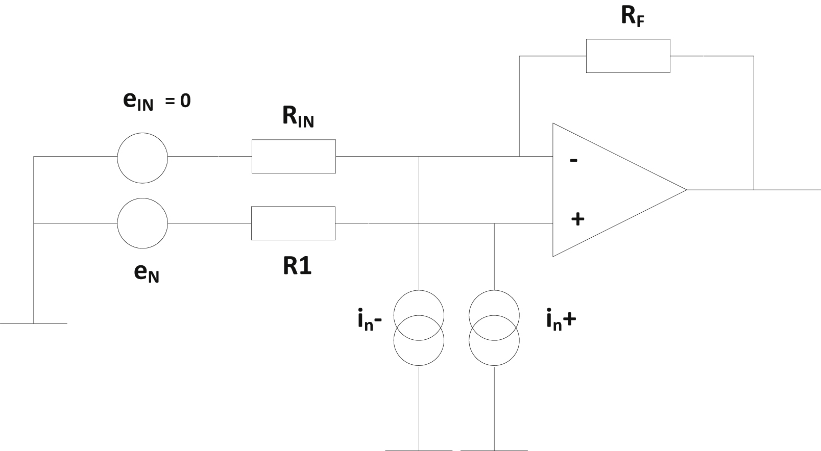
Amplifier noise is what you will find specified in the data sheet (sometimes; where it is not specified it can be two to four times worse than an equivalent low-noise part). It is characterized as a voltage source in series with one input, and a current source in parallel with each input, with the amplifier itself being considered noiseless. The values are specified at unity bandwidth, as RMS nanovolts or nanoamps per root-hertz; alternatively they may be specified over a given bandwidth. Because you need to add together all noise contributions, it is usually easiest to calculate them at unity bandwidth and then multiply the overall result by the square root of the bandwidth. This assumes a constant noise spectral density over the bandwidth of interest, which is true for resistors but may not be for the op-amp (see later). Noise, being statistical, is added on a root-mean-square basis. So the general noise model for an op-amp circuit is as shown in Fig. 5.17.
Figure 5.17 The Op-Amp Noise Model.
Contributor
Cause
Output Voltage Contribution
RIN
Thermal noise
(4kTRIN)−−−−−−−−√×AV×B−−√=N(RIN)
R1
Thermal noise
(4kTR1)−−−−−−−√×(AV+1)×B−−√=N(R1)
RF
Thermal noise
(4kTRF)−−−−−−−√×B−−√=N(RF)
in−
Amplifier current noise
in−×RF×B−−√=N(in−)
in+
Amplifier current noise
in+×R1×(AV+1)×B−−√=N(in+)
en
Amplifier voltage noise
en×(AV+1)×B−−√=N(en)
Total output noise=√[N(RIN)2+N(R1)2+N(RF)2+N(in−)2+N(in+)2+N(en)2]
When the noise is added in RMS fashion, if any noise source is less than a third of another it can be neglected with an error of less than 5%. This is a useful feature to remember with complex circuits where it is difficult to account accurately for all generator resistances.
Figure 5.18 Standard Op-Amp Inverting Amplifier.
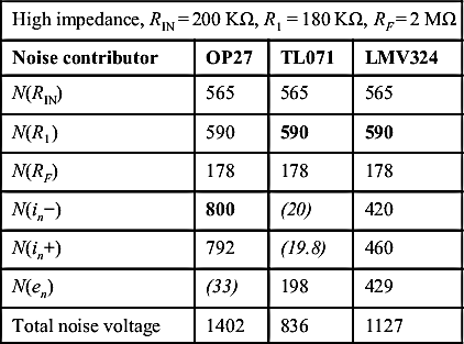
As an example of how to apply the noise model, let us examine the trade-offs between a high-impedance and a low-impedance circuit for different op-amps. The circuit is the standard inverting configuration with R1 sized according to the principle laid out earlier for minimization of bias current errors (R3 in Fig. 5.4). RIN is the sum of generator output impedance and amplifier input resistor (Fig. 5.18). The op-amps chosen have the following noise characteristics (at 1kHz):
Working from the noise model of Fig. 5.15, the contributions (in nV/√Hz) are tabulated for a low-impedance circuit and a high-impedance circuit, with the major contributor in each case shown emphasized and the negligible contributors shown in brackets:
Low impedance, RIN=200Ω, R1=180Ω, RF=2KΩ
Noise contributor
OP27
TL071
LMV324
N(RIN)
17.9
17.9
17.9
N(R1)
18.7
18.7
18.7
N(RF)
(5.6)
(5.6)
(5.6)
N(in−)
(0.8)
(0.02)
(0.42)
N(in+)
(0.79)
(0.02)
(0.46)
N(en)
33
198
429
Total noise voltage
41.9
200
430
High impedance, RIN=200KΩ, R1=180KΩ, RF=2MΩ
Noise contributor
OP27
TL071
LMV324
N(RIN)
565
565
565
N(R1)
590
590
590
N(RF)
178
178
178
N(in−)
800
(20)
420
N(in+)
792
(19.8)
460
N(en)
(33)
198
429
Total noise voltage
1402
836
1127
Some further rules of thumb follow from this example:
• high-impedance circuits are noisy
• in low-impedance circuits, op-amp voltage noise will be the dominant factor
• in high-impedance circuits, one or other of resistor noise or op-amp current noise will dominate: use a biFET or CMOS device and delete R1
• do not expect a low-noise voltage op-amp to give you any advantage in a high-impedance circuit
Noise Bandwidth
Deciding the actual noise bandwidth is not always simple. The bandwidth used in the noise calculations is a notional “brick-wall” value, which assumes infinite attenuation above the cut-off frequency. This of course is not achievable in practice, and the circuit bandwidth has to be adjusted to reflect this fact. For a single-pole response with a cut-off frequency fc and a roll-off of 6dB/octave, the noise bandwidth is 1.57fc. For a cascade of single-pole filters the ratio of the noise bandwidth to cut-off frequency decreases.
For more complex circuits it is usually enough to make some approximation to the actual bandwidth. If the low-frequency cut-off is more than a decade below the high-frequency one then it can be neglected with little error, and the noise bandwidth can be taken as from dc to the high-frequency cut-off. The exception to this is in very low–frequency and dc applications (below a few tens of hertz), because at some point the op-amp noise contribution starts to rise with decreasing frequency. This region is known as 1/f or “flicker” noise. All op-amps show this characteristic, but the point at which the noise starts to rise (the 1/f noise corner) can be reduced from a few hundred hertz to below 10Hz by careful design of the device.
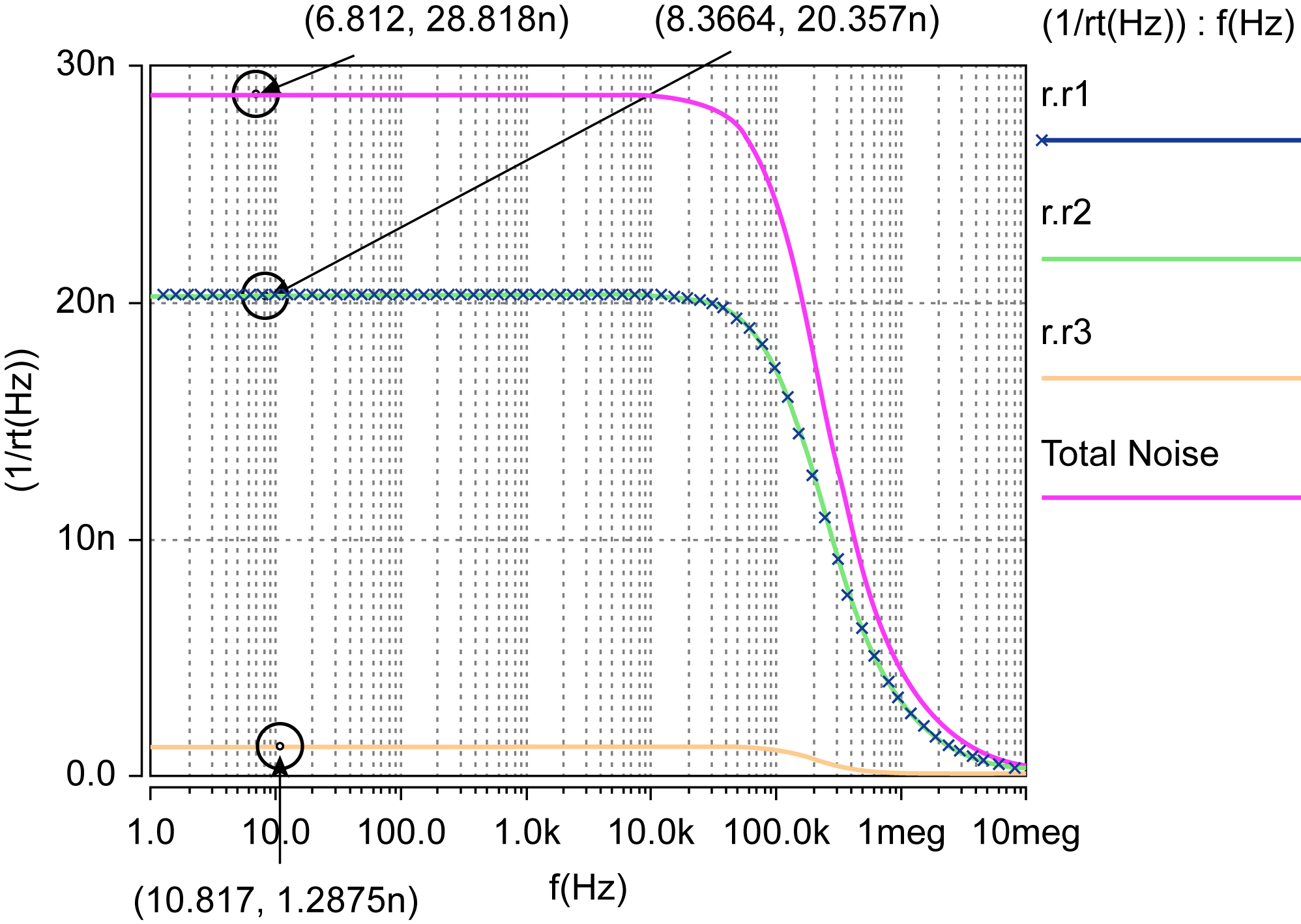
Modeling and Simulation of Noise
Luckily, we have the option to carry out noise analysis using simulations, and we have two choices to consider when we do that. The first option is to add random noise sources that have the correct RMS value of noise and complete time domain simulations, and while this is very accurate, it is also extremely time consuming to complete. The second option is to work in the frequency domain, and in this way the noise analysis in a simulators works like a small-signal frequency analysis (ac) by sweeping the frequency and plotting the output. In the noise analysis, however, unlike the conventional frequency analysis, the sum of the individual noise contributions over the frequency range specified is calculated.
This is particularly useful in situations such as the example we have just considered, where there is a frequency dependence in the characteristic, and as such it would be a laborious task to calculate the overall frequency behavior, whereas in a simulator, a single analysis will give that response.
If we implement the circuit in a circuit simulator (in this case Saber) then the noise voltage spectral response can be simulated.
As we know from the circuit in our previous example (potential divider and simple amplifier, plus low-pass filter), there is a low-pass filter on the output, and the noise is subject to the same filtering as the signal, so it is a useful check to see that the noise response exhibits the same low-pass response. If we compare the overall noise at a low frequency, we can see that the simulator predicts a value for the noise voltage RMS of 28.818nV/√Hz, which is entirely consistent with our calculated value.
5.2.14. Supply Current and Voltage
Circuit diagrams often leave out the supply connections to op-amp packages, for the very good reason that they create extra clutter, and the purpose of a circuit diagram is to communicate information as clearly as it can. When a single supply or a dual-rail supply is used throughout a circuit then confusion is unlikely, but with several different voltage levels in use it becomes difficult to work out exactly which op-amp is supplied by what voltage, and it is then better practice to show supplies to each package.
Supply Voltage
By far the largest number of recent op-amp introductions is aimed at low-power, single-supply applications where the circuit is battery operated. The lithium battery voltage of 3V is a major driving force in this trend. Although “low power” and “single supply” are independent parameters, they usually coexist as circuit specifications. A few years ago, op-amps were associated with ±15V supplies, which shrank to ±5V then to just +5V; now, nominal +3V supplies are common, with surprisingly little sacrifice in device performance. But low-power, low-voltage devices are not as forgiving of system design shortcomings because they have less input range to accommodate poorly behaved input signals, less head room to deal with dynamic range requirements, and less output drive capacity. System design decisions should still favor higher voltage rails where these are possible.
Supply Current
One of the disbenefits of not showing supply connections is that it is easy to forget about supply current (IS). Data sheets will normally give typical and maximum figures for IS at a specified voltage and no load. If the supply voltages are the same in the circuit as on the data sheet, and if none of the outputs are required to deliver any significant current, then it is reasonable just to add the maximum figures for all the devices in circuit to arrive at a worst-case power consumption. At other supply voltages, you will have to make some estimate of the true supply current, and some data sheets include a graph of typical IS versus supply voltage to aid in this. Also, note that IS varies with temperature, usually increasing with cold.
When an op-amp output drives a load, be it resistive, capacitive or inductive, the current needed to do so is drawn from one supply rail or the other, depending on the polarity of the output. In the worst case of a short-circuit load, IS is limited by the device's output current limiting. It is quite possible for the load currents to dominate power supply drain. With typical quiescent IS figures of a milliamp or so, you only need an output load resistance of 10kΩ being driven with a ±10V swing to double the actual current consumption of the circuit. When calculating worst-case load currents in these circumstances, you need to know not only the maximum output swing into resistive loads but also the current that may be needed to drive capacitive loads.
lS Versus Speed and Dissipation
Op-amp supply current is usually a trade-off against speed. You can find devices that are spec'd at 10μA IS, but such a part can only offer a slew rate of 0.03V/μs. Conversely, fast devices require more current, often up to 10mA. At these levels, package dissipation rears its head. An op-amp run at ±15V with 10mA IS is dissipating 300mW. With a thermal resistance of 100–150°C/W (the data sheet will give you the exact value) its junction temperature will be 30–45°C above ambient (see Section 9.5.1), and this is before it drives any load! This could well prevent the use of the part at high ambient temperatures and will also affect other parameters that are temperature sensitive. With such a device, make sure you know what its operating temperature will be before getting deeply involved in performance calculations.
5.2.15. Temperature Ratings
And so we come naturally to the question of over what temperature range can you use a particular device. Analog ICs historically have been marketed for three distinct sectors, with three specified temperature ranges:
• Commercial: 0 to +70°C
• Industrial: −40 to +85°C (occasionally −25 to +85°C)
• Military: −55 to +125°C
The picture is nowadays slightly blurred with the introduction of parts for the automotive market, which may be spec'd over −40 to +125°C, and with some Japanese suppliers (predominantly in the digital rather than analog area) offering nonstandard ratings such as −20 to +75°C.
If you are designing equipment for the typical commercial environment of 0–50°C then you are not going to worry much about device temperature ratings: just about every IC ever made will operate within this range. At the other extreme, if you are designing for military use then you will be buying military-qualified components, paying the earth for them, and this book will be of little use to you. But the question quite frequently arises, what parts should I use when my ambient temperature range goes a few degrees below 0 or above 70°C?
In theory, you should use industrial temperature–rated devices. Unhappily, there are three good reasons why you might not:
• the part you want to use may not be available in the industrial range;
• if it is available, it may be too expensive;
• even if it is listed as available, it may actually prove to be on a long lead-time or otherwise hard to get.
So the question resolves itself into: can I use commercial parts outside their specified temperature range? And the answer is: maybe. No IC manufacturer will give you a guarantee that the part will operate outside the temperature range that he specifies. But the fact is, most parts will, and there are two main factors that limit such use, namely specifications and reliability.
Specification Validity
The manufacturer will specify temperature-sensitive parameters (which is most of them) either at a nominal temperature (25°C) or over the temperature range. These specifications have bite, in that if the part fails to meet them the customer is entitled to return it and ask for a replacement. So the manufacturer will test the parts at the specification limits. However, he is not responsible for what happens outside the temperature range, and it is more than likely that some parameters will drift out of their specification when the temperature limits are overstepped. Very often these parameters are unimportant in the application, such as offset voltage in an ac amplifier. Therefore you can, with care, design a circuit with wider tolerances than that would be needed for the published figures and trust that these will be sufficient for wide temperature range abuse.
It is of course a risky approach, and two extra risks are that some parameters may change much more outside the specified temperature range than they do within it, and that you may successfully test a sample of manufacturer A's product, but manufacturer B's nominally identical parts behave quite differently. We shall comment on this again in Section 5.2.15.
Package Reliability
The second factor is reliability. The reliability of any semiconductor device worsens with increasing temperature; a temperature rise of 10°C halves the expected lifetime. So operating ICs at high temperatures is to be avoided wherever possible, but there is no magic cut-off at 70 or 85°C. The maximum junction temperature should always be observed, but this is usually in the region of 100–150°C.
At low temperatures the problem is included moisture. Molded plastic packages allow some moisture to creep along the lead-to-plastic interface (this is worse at high temperatures and humidities), and this can accumulate over the surface of the chip, where it is a long-term corrosive influence. When the operating temperature dips below 0°C the moisture freezes, and the resulting change in conductivity and volume can give sudden changes in parameters, which are well outside the drift specifications. The effect is very much less with “hermetic” packages using a glass–ceramic–metal seal, and in fact progress in plastic packages has advanced to the point where included moisture is not as serious a problem as it used to be. Other board-related problems arise when equipment is used below 0°C due to condensation of airborne moisture on the cold printed circuit board surface, as ambient temperature rises.
5.2.16. Cost and Availability
The subtitle to this section could be, why use industry standards? Basically, the application of op-amps (along with virtually all other components) follows the 80/20 rule beloved of management consultants: 80% of applications can be met with 20% of the available types. These devices, because of their popularity, become “industry standards” and are sourced by several manufacturers. Their costs are low and their availability is high. The majority of other parts are too specialized to fulfill more than a handful of applications and they are only produced by one or perhaps two manufacturers. Because they are only made in small quantities their cost is high, and they can sometimes be out of stock for months.
When to Use Industry Standards
The virtue of selecting industry standards is that the parts are well established, unlikely in the extreme to run into sourcing problems or be withdrawn (the humble 741 has been around for over 30years!) and, because of the competition between manufacturers, they will remain cheap. If they will do the job, use them in preference to a sole-sourced device. For companies with many different designs of product, keeping the variety of component parts low and reusing them in new designs has the benefit of increasing the total purchase of any given part. This potentially reduces its price further.
Another hidden advantage of older, more established devices is that their quirks and idiosyncrasies are well known to the suppliers' applications support engineers, and you are less likely to run into unusual effects that are peculiar to your usage and that take days of design time to resolve.
But nothing comes for free: the negative aspect of multisourcing is that many parameters go unspecified for cheap devices, and this leaves open the possibility that different manufacturers' nominally identical parts can differ substantially in those parameters that are omitted from the common spec. If you have designed and tested a circuit with manufacturer A's devices, and they happen to be quite fast, you will be heading for production problems when your purchasing manager buys a few thousand of manufacturer B's devices that are slower. For instance, TI's data sheet for the LM324 gives a typical slew rate of 0.5V/μs at 5-V supply; but National, who could fairly be said to have invented the part, do not mention slew rate at all in theirs.
To deal with this, design the circuit from the outset to be insensitive to those parameters that are badly specified, unspecified or (worse) specified differently in the data sheets of each manufacturer. Or, look for a more tightly specified part.
When Not to Use Industry Standards
Within the last few years there has been a countertrend to the imperative for multisourcing, and the use of industry standards. Hundreds of new types have been introduced, and many of them are much better than their predecessors. They not only minimize the trade-offs between speed, power, precision and cost but are also more fully specified. You can select a part by function and application—for instance, a DAC buffer or 75-Ω cable driver—rather than by comparing technologies, or by looking at a particular specification such as gain-bandwidth product. Following the manufacturer's selection guides on the basis of application will often lead quickly to the most suitable part.
Selecting more application-specific ICs in this way steers the design process away from industry standards. But there are a number of reasons why alternate sourcing has become less of a necessity, despite its advantages given above. The average product life cycle—sometimes months rather than years—is much shorter than the lifetime of a good op-amp. In addition, qualifying multiple sources is a task that many designers do not have time or expertise to do fully. Finally, for highly competitive products, you will have to choose parts that give your design the edge (even if they are proprietary) and for which there may be nothing comparable in performance, cost, or functionality.
Quad or Dual Packages
Comparing prices, the LM324 does offer, in fact, the lowest cost-per-op-amp (5p). This points up another factor to bear in mind when selecting devices: choose a quad or dual package in preference to a single device, when your circuit uses several gain stages. This reduces both unit cost and production cost. Such parts often have quiescent supply currents only slightly greater than a single-channel device, but with better offset, temperature tracking of drift, matching, and other specs. The disadvantages are inflexibility in supply voltage and pc layout, and possible thermal, power rail, or RF interaction between gain blocks on a single substrate.
Some parts are available only in dual or quad configurations because single-channel versions would not have enough applications. Conversely, highest speed op-amps, with bandwidths above several hundred megahertz, are often available in singles only, because of internal cross talk. However, pinouts in multichannel configurations are less standardized than the basic single-channel unit, so substitutes are harder to find.
5.2.17. Current-Feedback Op-Amps
There are also op-amps that use current-feedback topology instead of the more familiar voltage feedback. Voltage feedback is the classic, well-understood mechanism, which we have been discussing all the way through this section so far. In current feedback, the error signal is a current flowing into the inverting input; the input buffer's low impedance, in contrast to a voltage amplifier's high input impedance, allows large currents to flow into it with negligible voltage offset. This current is the slewing current, and slew rate is a function of the feedback resistor and change in output voltage. Therefore, the current-feedback amplifier has nearly constant output transition times, regardless of amplitude.
A very small change in current at the inverting input will cause a large change in output voltage. Instead of open-loop voltage gain, the current-feedback op-amp is characterized by current gain or “transimpedance” ZS. As long as ZS>>RF, the feedback resistor, the steady-state (nonslewing) current at the inverting input is small, and it is still possible to use the usual op-amp assumptions as initial approximations for circuit analysis, i.e., the differential voltage between the inputs is negligible, as is the differential current (Fig. 5.20).
Figure 5.19 Noise Voltage Spectral Response Using a Simulated Noise Analysis.
Figure 5.20 The Current-Feedback Circuit.
In performance, current feedback generally offers higher slew rate for a given power consumption than voltage feedback, and voltage feedback offers you flexibility in selecting a feedback resistor, two high-impedance inputs, and better dc specifications. With a current-feedback op-amp, you first set the desired bandwidth via the feedback resistor, and then the gain is set according to the usual resistive ratios. This means that the wider the bandwidth, the lower will be the operating impedances. If RF is doubled, the bandwidth will be halved. The circuit becomes less stable when capacitance is added across the feedback resistor.
Current-feedback devices tend to be used only at higher frequencies, for applications such as professional video and high-performance wideband instrumentation. The same part can be used in several applications for quantity cost savings, using only as much bandwidth as needed. They are less common in lower end consumer applications because they need more design expertise. Current feedback is no “better” or “worse” than voltage, which is also capable of similar performance in the right design, but it does provide an alternative that is worth considering in the appropriate application.
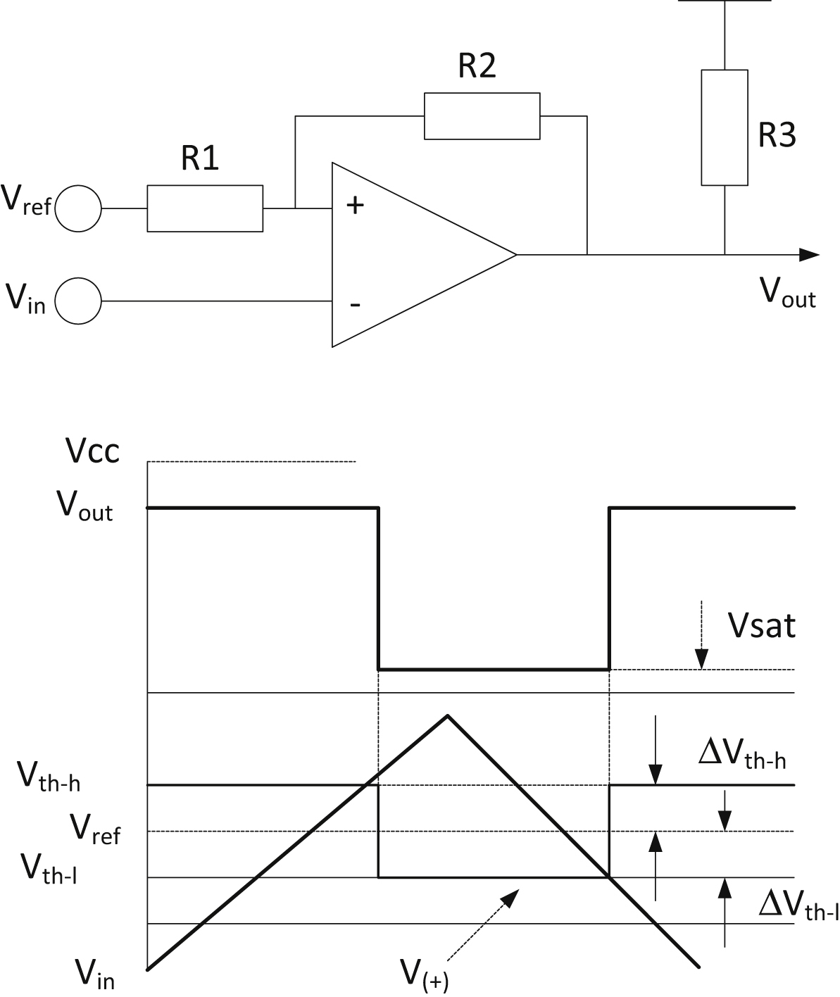
5.3. Comparators
A comparator is just an op-amp with a faster slew rate, and with its output optimized for switching. It is intended to be used open-loop, so that feedback stability considerations do not apply. The device exploits the very large open-loop gain of the op-amp circuit so that the output swings between “fully-on” and “fully-off”, depending on the polarity of the differential input voltage, and there should be no stable state in between. Input-referred and open-loop parameters—offsets, bias currents, temperature drift, noise, CMRR, and PSRR, supply current and open-loop gain—are all specified in the same way as op-amps. Output and ac parameters are specified differently.
5.3.1. Output Parameters
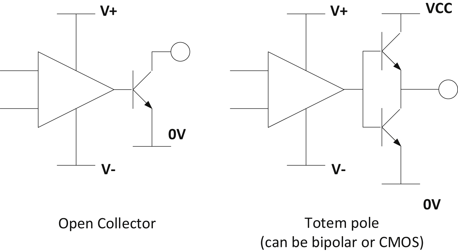
The most frequent use of a comparator is to interface with logic circuitry, so the output circuit is designed to facilitate this. Two configurations are common: the open collector, and the totem pole (Fig. 5.21). The open-collector type requires a pull-up resistor externally, while the totem pole does not. Both types interface readily to the classical LSTTL logic input, which requires a higher pull-down current than is needed to pull it up. The CMOS input, which only takes a small current at the transition due to its input capacitance, is even easier. The output is specified either in terms of its saturation voltage, sink current, leakage current, and maximum collector voltage for the open-collector type or in terms of high- and low-level output voltages at specified load currents for the totem-pole type.
Figure 5.21 Comparator Outputs.
Because the totem-pole type is invariably aimed at logic applications, it is always specified for 3.3 or 5V output levels. The open-collector type, which includes the highly popular LM339/393 and its derivatives, is more flexible since any output voltage can be obtained simply by pulling up to the required rail, which can be separate from the analog supply rails.
5.3.2. AC Parameters
Because the comparator is used as a switch, the only ac parameter that is specified is the response time. This is the time between an input step function and the point at which the output crosses a defined threshold. It includes the propagation delay through the IC and the slewing rate of the output. Outside of the device itself, two factors have a large effect on the response time:
• the input overdrive
• the output load impedance.
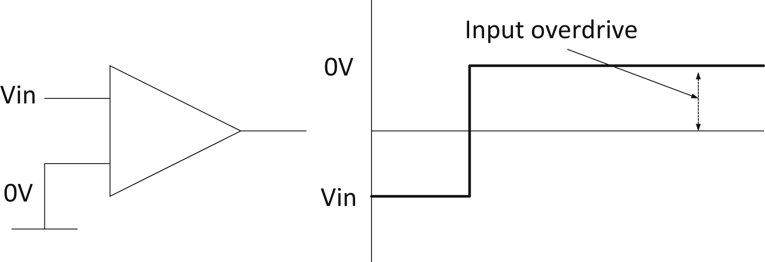
Overdrive
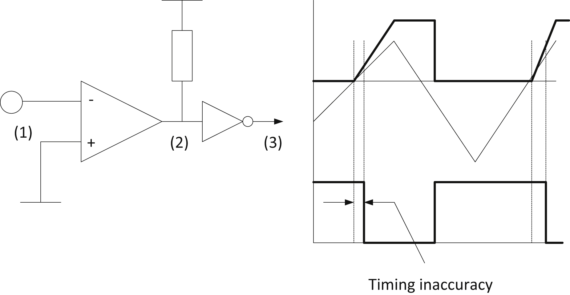
For the specifications, an input step function is applied, which forces the differential input voltage from one polarity to the other. The overdrive, as in Fig. 5.22, is the final steady-state differential voltage. Usually, the step amplitude is held constant, and its offset is varied to give different overdrive values. The greater the overdrive, the more current is available from the differential input stage to propagate the change of state through to the output, although beyond a certain point there is no gain to be had from increasing it. Small overdrives can lead to surprisingly long response times, and you should check the data sheet carefully to see if the device is being specified in similar fashion to how your circuit will drive it.
The specification test assumes that the step function has a much shorter rise time than the response to be measured. Response time specs are virtually meaningless when the comparator is driven by slow rise time analog signals. We shall discuss this more fully under the heading of hysteresis.
Figure 5.22 Comparator Overdrive.
Load Impedance
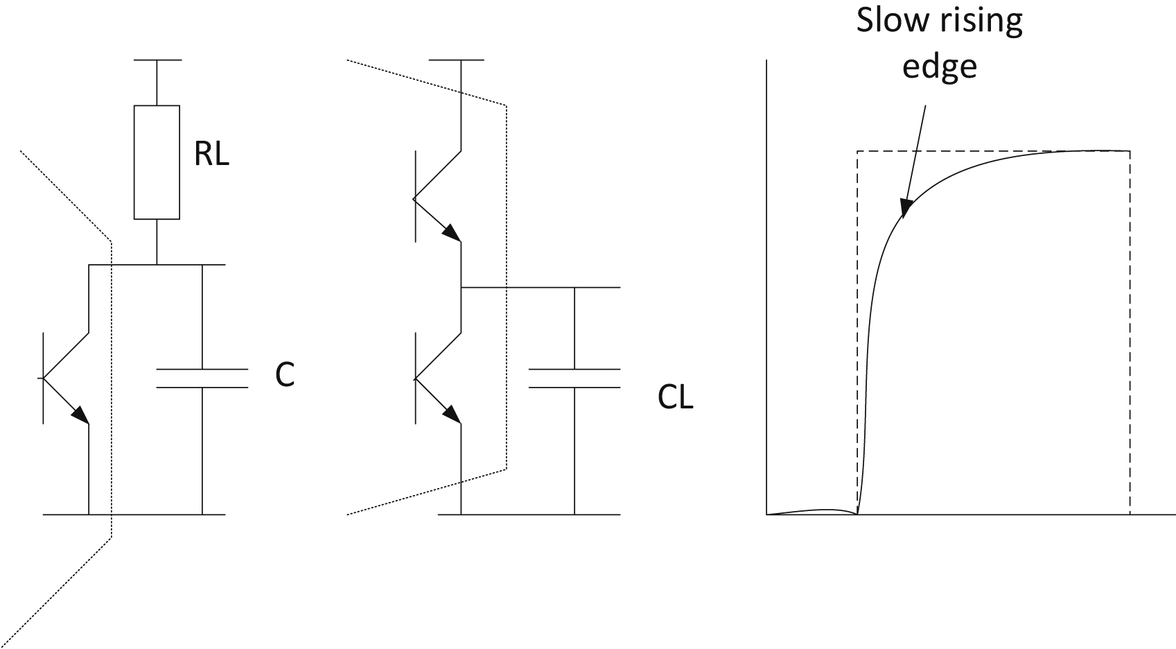
The output load resistance RL (for open-collector types) and capacitance CL have a major influence on the output slewing rate. The capacitance includes the device output capacitance, circuit strays and the input capacitance of the driven circuit (this last is usually the most significant). The slewing rate is determined by the current that is available to charge and discharge the capacitance, following the rule dV/dt=I/C. For the negative-going transition this current is supplied by the output sink transistor and is in the region of 10–50mA, assuring a fast edge, but the current available to charge the positive transition is supplied by the pull-up device or resistor and may be an order of magnitude lower. The choice of output resistor directly affects the positive-going rise time (Fig. 5.19) and the power dissipation of the circuit (Fig. 5.23).
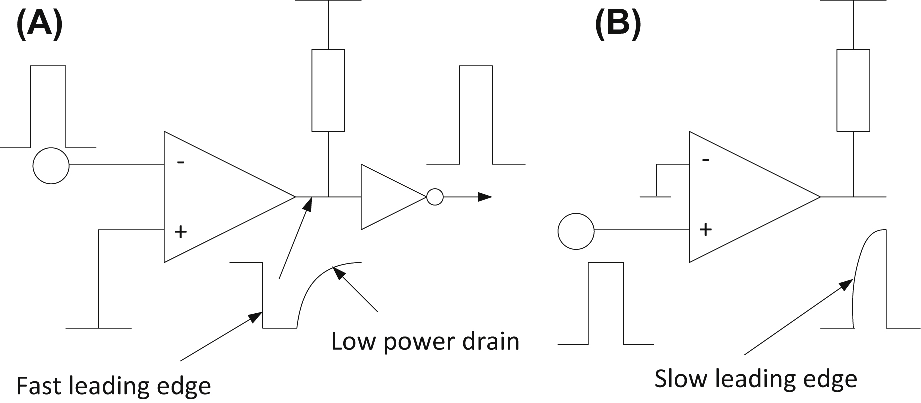
The Advantages of the Active Low
On this latter point, it is worth remembering that if you expect low duty–cycle pulses at the output, want low power drain and a fast leading edge and have a choice of logic polarity, that the preferable configuration is to use an active low output as in Fig. 5.24A. The signal is normally off so that power drain is low, and the leading edge transition depends on the output transistor rather than the pull-up. If a fast trailing edge is also needed, the pull-up can be reduced in value without significantly affecting power drain if the duty cycle is low. It is easy and cheap to provide a logic inverter if you really need positive-going pulses.
Pulse Timing Error
Continuing this train of thought, you can see that it is quite easy for the pulse timing to be affected by the output rise- and fall-times. This is quite often the source of unexpected errors in circuits, which convert analog levels into pulse widths for timing measurement. Because the pulse rising edge is slowed to a greater extent than the falling edge, the point at which it crosses the following logic gate's switching threshold is different, so that rising and falling analog inputs result in different switching points. This effect is demonstrated in Fig. 5.25. The problem is generally more visible with CMOS-input-level gates than it is with TTL-input-level ones, as TTL's switching threshold is closer to 0V whereas the CMOS threshold is ill-defined, being anywhere between 0.3 and 0.7 times its supply rail. The difference can amount to a microsecond or more in low-power circuits.
Figure 5.23 Output Slewing Versus Load Capacitance.
You may often be faced with a circuit full of multiple op-amp packages and the need for a single comparator. Rather than invest in an extra package for the comparator function, it is quite to use a spare op-amp as a comparator with the following provisos:
Figure 5.25 Timing Error Through Pull-Up Delay.
• The response time and output slew rate are adequate. Typical cheap op-amp slew rates of 0.5V/μs will traverse the logic “gray area” from 0.8 to 2V in about 3μs; this is too slow for some logic functions. Faster op-amps make better comparators.
• In some op-amps, recovery from the saturated state can take some time, causing appreciable delays before the output starts to slew. This is hardly ever specified on data sheets.
• The output voltage swing and drive current are adequate and correct for the intended load. Clearly you cannot drive 5-V logic directly from an op-amp output that swings to within 2V of ±15V supply rails. Some form of interface clamping is needed; this could take the form of a feedback zener arrangement so that the output is not allowed to saturate, which confers the additional benefit of reduced response time. Drive current is not a problem with CMOS inputs.
It is also possible, if you have to, to use a comparator as an op-amp. (In most cases: some totem-pole outputs cannot be operated in the linear mode without drawing destructively large supply currents.) It was never designed for this, and will be hideously unstable unless you slug the feedback circuitry with large capacitors, in which case it will be slow. Also, of course, it is not characterized for the purpose, so for some parameters you are dealing with an unknown quantity. Unless the application is completely noncritical it is best to design op-amp circuits with op-amps.
5.3.4. Hysteresis and Oscillations
When the analog input signal is changing relatively slowly, the comparator may spend appreciable time in the linear mode while the output swings from one saturation point to the other. This is dangerous. As the input crosses the linear-gain region the device suddenly becomes a very high–gain open-loop amplifier. Only a small fraction of stray positive feedback is needed for the open-loop amplifier to become a high-frequency oscillator (Fig. 5.26).
Figure 5.26 Oscillation During Output Transitions.
The frequency of oscillation is determined by the phase shift introduced by the stray feedback and is generally of the same order as the equivalent unity-gain bandwidth. This is not specified for comparators, but for typical industry-standard devices is several of MHz. The term “relatively slowly” as used above means relative to the period of the oscillation, so that any traverse of the linear region, which takes longer than a few hundred nanoseconds must be regarded as slow: this of course applies to a very large proportion of analog input signals!
The Subtle Effects of Edge Oscillation
This oscillation can be particularly troublesome if you are interfacing to fast logic circuits, especially when connecting to a clock input. It can be hard to spot on an oscilloscope, as you will probably have the time base set low for the analog signal frequency, but the oscillations appear to the digital input as multiple edges and are treated as such: so for instance a clock counter might advance several counts when it appears to have had only one edge, or a positive-going clock input might erroneously trigger on a negative-going edge.
Even when you do not have to contend with high-speed logic circuits, the oscillation generated by the comparator can be an unexpected and unwelcome source of RF interference.
Minimize Stray Feedback
The preferred solution to this problem is to reduce the stray feedback path to a minimum so that the comparator remains stable even when crossing the linear region. This is achieved by following three golden rules:
• keep the input drive impedance low;
• minimize stray feedback capacitance by careful layout; and
• avoid introducing other spurious feedback paths, again by careful layout and grounding.
The lower the input impedance, the more feedback capacitance is needed to generate enough phase shift for instability. For instance, 2pF and 10kΩ gives a pole frequency of 8MHz, a perfectly respectable oscillation frequency for many high-speed comparators. It is hard to reduce stray capacitance much below 2pF, so the moral is, keep the drive impedance below 10kΩ, and preferably an order of magnitude lower.
Minimum stray capacitance from output to input should always be the layout designer's aim; follow the rules quoted in Section 5.2.10 for high-frequency op-amp stability. Most IC packages help you in this regard by not putting the output pin close to the noninverting input pin. Do not look this particular gift horse in the mouth by running the output track straight back past the inputs! Guarding the inputs (see Section 2.4.1) can be useful. And, again as with op-amp circuits, do not introduce ground-loop or common-mode feedback paths by incorrect layout.
Figure 5.27 Hysteresis.
Ignoring input and output leakage currents
Vout (H)=Vcc−(Vcc−Vref)(R3/[R1+R2+R3])
Vout (L)=Vsat
Vth-h=α×Vcc+(1+α)×Vref where α=R1/(R1+R2+R3)
ΔVth-h=α×(Vcc+Vref)
Vth-l=β×Vsat+(1−β)×Vref where β=R1/(R1+R2)
ΔVth-l=β×(Vsat−Vref)
A common simplification is that R3<<R1+R2 so that α=β, and that Vref is half of Vcc and Vsat=0, in which case ΔVth (the total hysteresis band) reduces to β×Vcc.
Hysteresis
Another approach to the problem of unwanted oscillation is to kill it with hysteresis. This approach is used when the above methods fail or cannot be applied, and you can also use it as a legitimate circuit technique in its own right, as in the well-known Schmitt trigger. Hysteresis is the application of deliberate positive feedback to propel the output speedily and predictably through the linear region. The principle of hysteresis is shown in Fig. 5.27.
Note that although this looks superficially like the classic inverting op-amp configuration, feedback is applied to the noninverting input and is therefore operating in the positive sense. Note also that the application of hysteresis modifies the switching threshold in both directions, and that it is modified differently in either direction by the presence of R3. This resistor is shown in the circuit of Fig. 5.27 to emphasize that it must be included in calculating hysteresis; we have assumed that the comparator is the open-collector type. If the output is the totem-pole type, then R3 is omitted but the output levels and impedance must be taken into consideration. These values directly affect the switching threshold and can cause surprisingly large inaccuracies.
Because hysteresis deliberately alters the switching threshold, it cannot be indiscriminately applied to all comparator circuits to clean up their oscillatory tendencies, nor should it. The techniques outlined previously should be the first priority. But it is not always possible to keep drive impedances low and where high impedance is necessary, hysteresis is a valuable tool. If the minimum input dV/dt is predictable, you can also apply a judicious amount of ac hysteresis (by substituting a capacitor for R2), which will prevent oscillation without affecting the dc threshold: but beware of slow-moving inputs, or you will simply end up with a longer time-constant oscillator!
5.3.5. Input Voltage Limits
When an op-amp is operating in closed loop, the differential voltage at its inputs is theoretically zero. If it is not then the feedback loop is open, either by design or because of one or another form of overloading. Comparators on the other hand are intended for open-loop operation, and their differential input voltage is never expected to be zero.
Data sheets specify the maximum voltage range of differential input signals and this should not be overlooked. If it is exceeded, too much current through the breakdown of the input transistor base–emitter junctions (or MOS gates) can degrade the input offset and bias current parameters. Most of the industry-standard LM339 derivatives have a differential limit equal to the supply rail limit, but some comparators have quite restricted differential input ranges. For instance the fast NE529 has a differential input restriction of ±5V, with a common mode of ±6V. These two quantities interact: both inputs at +4V will satisfy the common-mode limit, but if one is left at +4V the other cannot be taken below −1V because the differential voltage is then greater than 5V.
Even if the normal operating differential range is kept within limits, it is possible for abnormal conditions (such as cycling of separate power rails) to breach the limit. If this is at all likely, and if the condition cannot be prevented, at the very least include some input current protection resistance. You can calculate the required values from the expected or possible overvoltage divided by the absolute maximum input current, or from the power dissipation, which is always quoted on device data sheets.
Comparator Parameters Versus Input Voltage
Also, while considering large differential input voltages, remember that unexpected things can happen to the comparator even when the limits are not exceeded. Response time is usually specified for a common-mode voltage of zero and may degrade when the common-mode limits are approached; this applies equally to bias currents. Some data sheets show curves of input bias current, which have step changes (Fig. 5.28) at certain differential input voltages, due to internal dc feedback. Notice these and make sure your circuit can cope!
Figure 5.28 Input Bias Current Steps.
In multichannel packages, some comparators may remain unused. Never leave unused inputs open, as that device could oscillate on its own, which would then be coupled into the other devices in the same package. If both inputs are grounded, the unpredictable offset voltage will mean that the output voltage, and hence unit supply current, will vary. The safest course is to ground one input and supply the other from another fixed voltage within its differential and common-mode limit (which might include the supply rail), so that the device is always saturated.
5.3.6. Comparator Sourcing
Exactly the same comments about sourcing apply to comparators as were made earlier about op-amps (see Section 5.2.15). Like the LM324 op-amp, the most popular and cheapest part per comparator is the quad LM339, with its dual counterpart the LM393 not far behind.
5.4. Voltage References
The need for a stable reference voltage is found in power supplies, measurement instrumentation, DAC/ADC systems and calibration standards. Two techniques exist to provide such references, one based on the precision zener diode and the other on the band-gap voltage of silicon.
5.4.1. Zener References
We have already discussed the operation of the basic zener diode (Section 4.1.7). To produce a reference from a zener, it must be temperature compensated, fed from a constant current and buffered. Temperature compensation is achieved by selecting a low-tempco zener voltage in the range 5.5–7V and mating it with a silicon diode so that the voltage tempcos cancel. The combination is driven from a constant current generator and buffered to give a constant output voltage regardless of load.
Since surface breakdown increases noise and degrades stability, a precision zener is usually fabricated below the surface of the IC, which contains its support circuitry, but this gives a greater spread of tempco and absolute voltage. The overall reference must therefore allow adjustment of these parameters, normally by laser wafer trimming. Such references can offer long-term stability of 50ppm/year and absolute accuracy of 0.1% with ±10ppm/°C tempco. Better performance is obtained if the reference can be stabilized with an on-chip heater, as in the LM399 for example. This takes a comparatively large power drain and has a warm-up time measured in seconds but offers sub-ppm tempcos.
5.4.2. Band-Gap References
A significant disadvantage of the zener reference is that its output voltage is set at around 6.9V and it therefore needs a comparatively high supply voltage. A competing type of reference overcomes this and other problems, notably cost and supply current, and has become extremely widespread since its invention by Robert Widlar in 1971. The fundamental circuit is shown in Fig. 5.29. In this circuit I1 and I2 differ by a fixed ratio and Vref is given (neglecting base currents) by
Vref=VBE3+I2×R2=VBE3+(VBE1−VBE2)R2/R1
(5.18)
Figure 5.29 The Band-Gap Reference.
The temperature coefficient of the second term can be arranged by suitable selection of I1, R1, and R2 to cancel that of the VBE3 term. This turns out to occur when Vref is in the neighborhood of 1.2V, which is equivalent to the “band-gap” voltage of a silicon junction at 0°K.
Such a band-gap reference, relying only on matched transistors, is easily integrated along with biasing, buffer, and amplifier circuitry to give a complete reference in a single package. It is capable of a lower minimum operating current and a sharper knee than any zener. As well as the unprocessed band-gap voltage of 1.2V (actual voltage depends on detailed internal design and process variations and varies between 1.205 and 1.26V) devices are available with trimmed outputs of 2.5, 5, and 10V, principally for use in digital-to-analog/analog-to-digital conversion circuits. Other voltages are available, and there are several adjustable parts offered as well.
Costs and Interchangeability
There is an obvious trade-off between initial voltage tolerance and tempco on the one hand, and cost and availability on the other, since the manufacturer has to accept a lower yield and longer test and trim time for the closer tolerances. Initial voltage can be trimmed exactly with a potentiometer, but this method adds both parts and production cost, which will offset the higher cost of a tighter tolerance part. Trimming the reference voltage can also worsen the reference temperature coefficient in some configurations, and there is the extra tempco of the trimming components to include. Table 5.2 shows a sample of typical two-terminal 1.2-V references, including their tolerance, tempco, minimum operating current and cost. Most of these are available in different grades, corresponding to tighter or looser tolerances and tempcos.
Table 5.2
Some Voltage References
Type
Output Voltage (V)
Tolerance
Tempco
Min. Current (μA)
Cost £, 25+
MAX6520EUR-T
1.2
±1%
20ppm/°C typ
50
1.29
LM4041B-1.2
1.225
±0.2%
100ppm/°C
45
0.97
ICL8069DCZR
1.23
±1.6%
100ppm/°C
50
0.78
ICL8069CCZR
1.23
±1.6%
50ppm/°C
50
1.27
LM385Z-1.2
1.235
±2%
20ppm/°C avg
10
0.30
LM385Z-1.2
1.235
±1%
20ppm/°C avg
10
0.55
LT1004CZ-1.2
1.235
±4mV
20ppm/°C
10
1.68
ZRA124A01
1.24
±1%
30ppm/°C
50
0.67
ZRA125F02
1.25
±2%
30ppm/°C
50
0.55
Although it would appear from this table that there is a wide choice of types offering much the same performance, not all of these are directly interchangeable. The minor differences in regulation voltage may catch you out if you have designed a circuit for a given voltage tolerance and subsequently want to change to a different type. The preferable solution is to allow as wide a tolerance as possible in the first place. Also, there are variations in the allowable or required capacitive loading. Some parts require a decoupling capacitor of 0.1−1μF across them, others require that such a capacitor is not included. The parts are mostly supplied in the TO-92 package or the small outline SOT23, but not all pinouts are the same. Again, check before specifying alternatives.
5.4.3. Reference Specifications
Line and Load Regulation
Line regulation is the change in output voltage due to a specified change in input voltage, normally quoted in microvolts per volt. Load regulation is a similar change due to a change in load current, expressed either in percent for a given current change or as a dynamic resistance in ohms. It should, but does not always, include self-heating effects due to dissipation change.
Output Voltage Tolerance
This is the deviation from nominal output voltage. It is quoted at a given temperature and input voltage or current, and the nominal voltage will differ under other conditions. Generally it is expressed as a percentage figure, but the asymmetry of device yields may persuade a manufacturer to quote upper and lower bounds and the nominal figure may not be in the middle of them. In your circuit design, it is best to ignore the nominal voltage and work everything out for upper and lower limits.
Output Voltage Temperature Coefficient
This is the output voltage change due to an ambient temperature difference, usually from 25°C. Because neither band-gap nor zener references exhibit a straight line voltage–temperature curve (see Fig. 5.26) manufacturers choose different ways to express their temperature coefficients, sometimes as an average value across the range in ppm/°C, sometimes as different values at a series of spot temperatures, and sometimes as a worst-case error band in mV. To evaluate different manufacturers' references properly you need to correct for these differences in specification (Fig. 5.30).
Long-Term Stability
Usually expressed in ppm/1000h or in microvolts change from the nominal voltage, this is a difficult specification to verify and so is often quoted as a typical figure based on characterization of a sample. It is rarely specified on the cheaper components. Zeners tend to stabilize after a couple of years, so for ultraprecision applications the practice of burning in zener references at high temperatures to speed up the settling process is sometimes followed.
Figure 5.30 Typical Band-Gap Reference Temperature Characteristics.
Settling Time
This is the time taken for the output to settle within a specified error band after application of power. It is typically in the tens-to-hundreds of microseconds region, and is normally only of interest if you are concerned about the dynamic performance of the reference circuit—for instance, if the application has to wake up rapidly from “sleep” mode. It does not include any long-term effects due to thermal shifts, but of course these do occur, more noticeably at higher operating currents.
Minimum Supply Current
The regulation of a two-terminal device is not maintained below a certain minimum current. Typical values for band-gap references are 50–100μA, with 10μA being available although some earlier devices are much higher than this. The very low useable operating currents combined with low dynamic resistance at these currents make band-gap devices very much preferable to zener types for low-power circuitry. The maximum operating current is usually based on the point at which the device goes outside its regulation specification, but may also be determined by allowable power dissipation.
5.5. Circuit Modeling
Virtually every op-amp supplier provides Spice models, which are a very useful approximation of device performance. There are two opposing criteria for such a model. It should use the fewest internal elements to ease computing, but it should also give an accurate representation of the device as a “black box.” You can use these models as a necessary (but not entirely sufficient) step in the design process. Models cannot capture a device's every sensitivity to supply variations or temperature and load changes. Dynamic performance such as slew rate and overshoot are especially difficult to model, and peculiarities such as behavior at or beyond the common-mode limits will be entirely absent.
The circuit design must be characterized for the entire range of performance characteristics that an off-the-shelf part might show, but generally available Spice models use typical rather than worst-case specs.
Even a perfect model would not capture what is just as critical in high-performance analog design: your physical circuit that surrounds the part. Just a few picofarads of circuit-board capacitance will change the frequency response, for example. Common impedances in the power or ground circuits (see Section 1.1) can affect stability and power supply rejection. Conductive residues on the circuit provide a leakage path between IC pins. No model of itself will detail your circuit layout strays or ground topology.
This does not mean you should not use manufacturer supplied models. Use them for initial assessments of your circuit, to about ±20% accuracy. At the same time, recognize that the model itself is neither perfect nor does it include the subtleties of your design. Check with the supplier to understand which modeled parameters are typical, which are worst case, which are at room temperature, and other similar limitations and simplifications. The typically short development timescale, and the project manager champing at the bit, may constrain your ability to experiment and tempt you to go straight from the model to the final layout. But if there is any critical performance issue that you know is not covered by the model, be prepared for a few design iterations, and do not be afraid to breadboard the design if possible.
Some modern simulators such as Saber have libraries of characterized parts, which have been built using much improved behavioral models, however, the limitation is always the accuracy of the source measured data used, and the limitations of using a small sample of parts to obtain that data.
The best advice for effective use of simulation is to use it to evaluate the initial design to the limits of accuracy defined earlier, and use advanced techniques such as Monte Carlo (statistical analysis) to establish the range of operation of the circuit, and see how well the component tolerance work across a wide range of scenarios, not just attempting to fine-tune the nominal case.
Most suppliers offer evaluation boards and suggested circuit-board layout drawings, especially for high-performance or complex parts. An evaluation board shows you what the part can do in a reference design. The layout can serve as a starting point for your own implementation, so you will not waste time discovering mistakes the application engineers have already made and dealt with. The first question an applications support engineer asks when a designer calls with a problem such as oscillation in high-frequency current-feedback circuits is, “Did you use the evaluation board layout?”
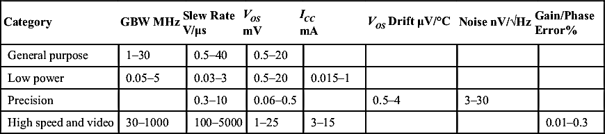


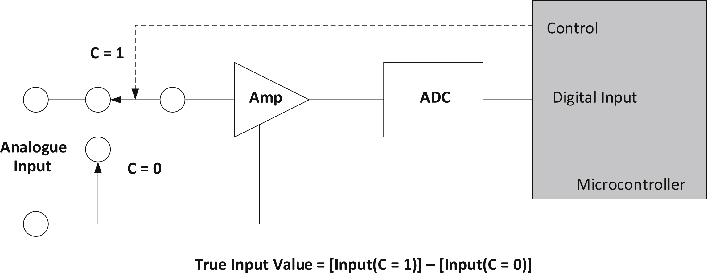


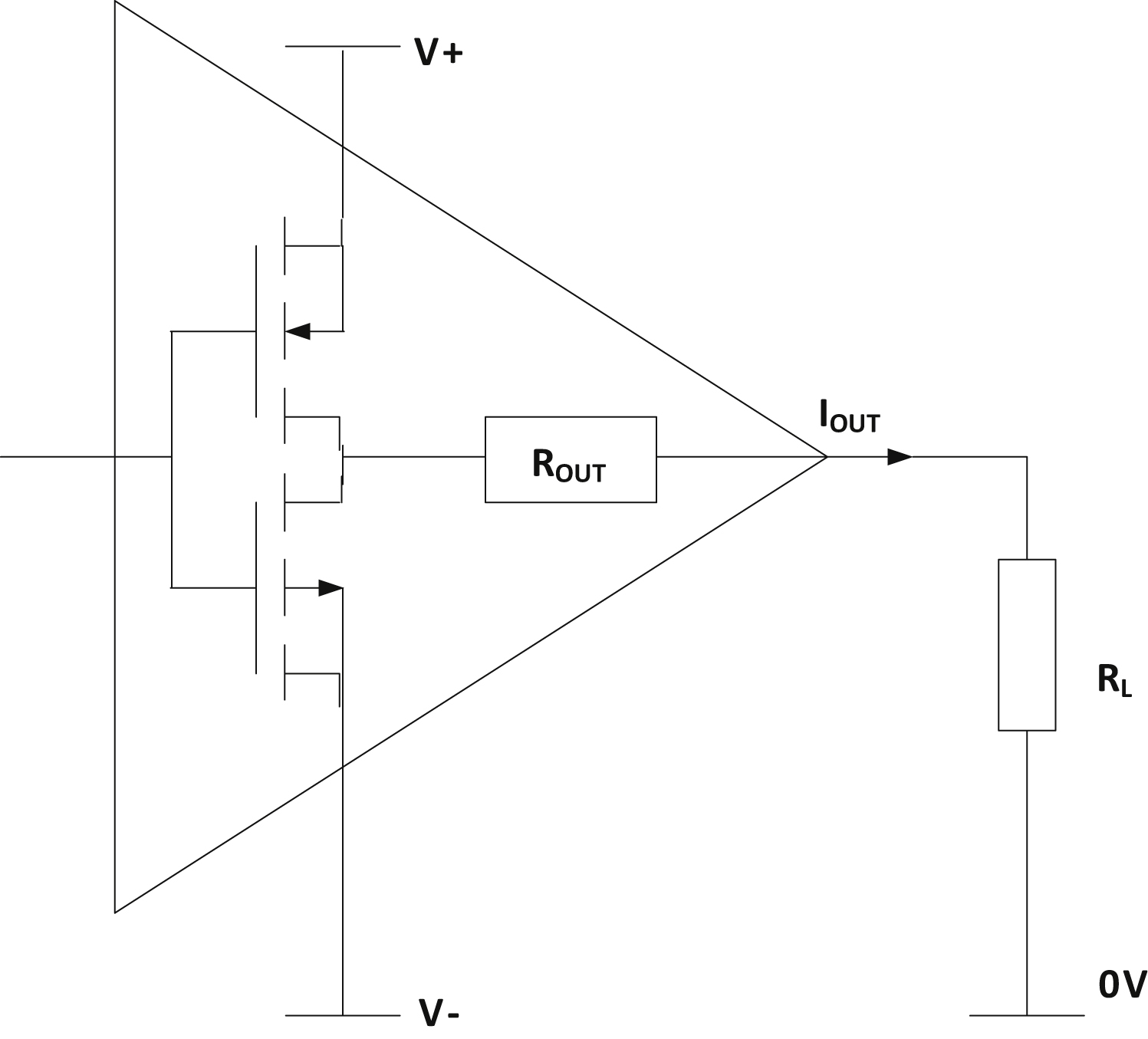
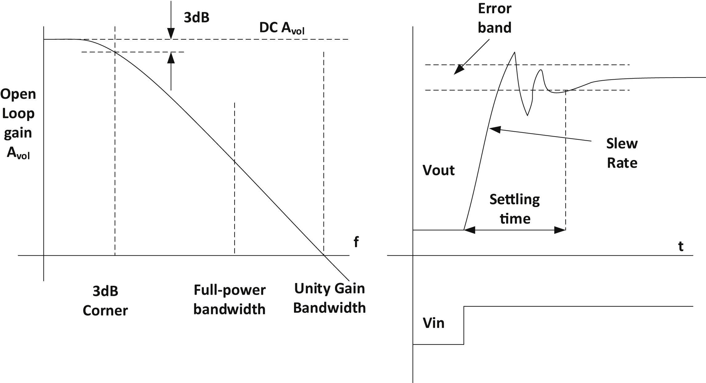

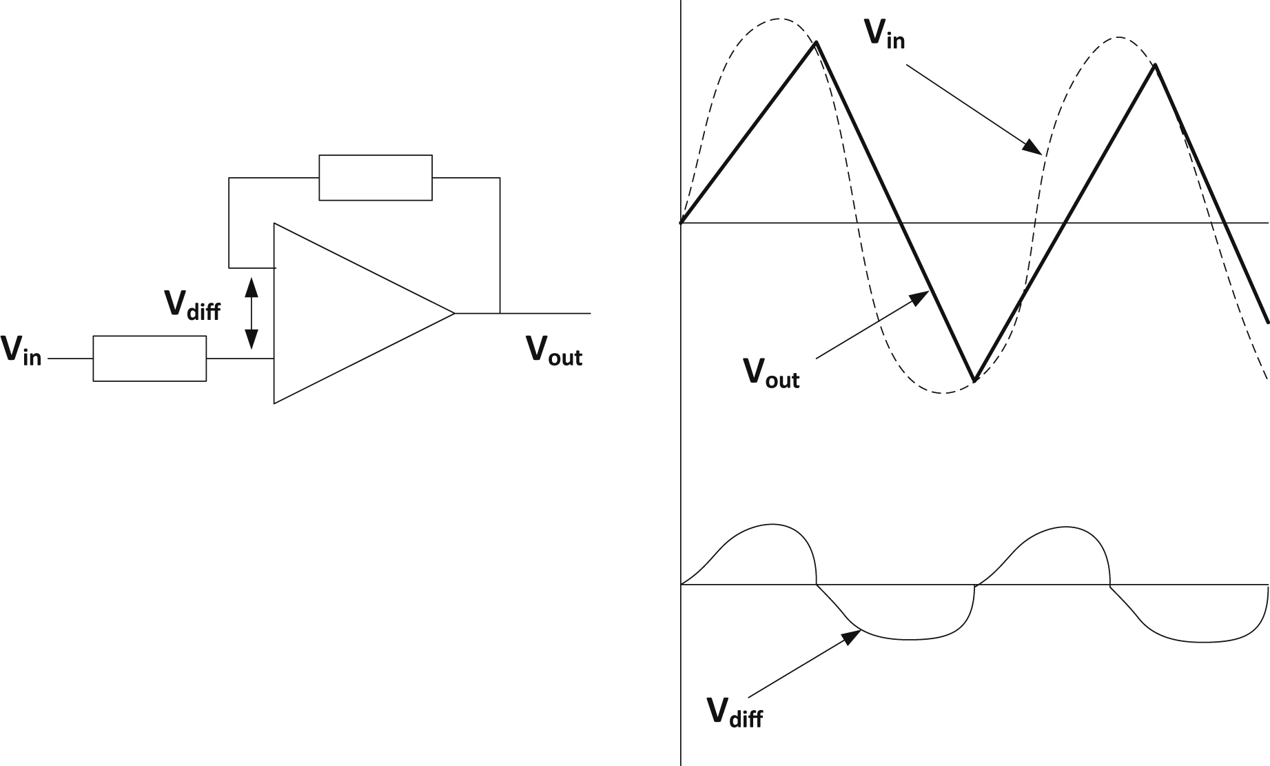
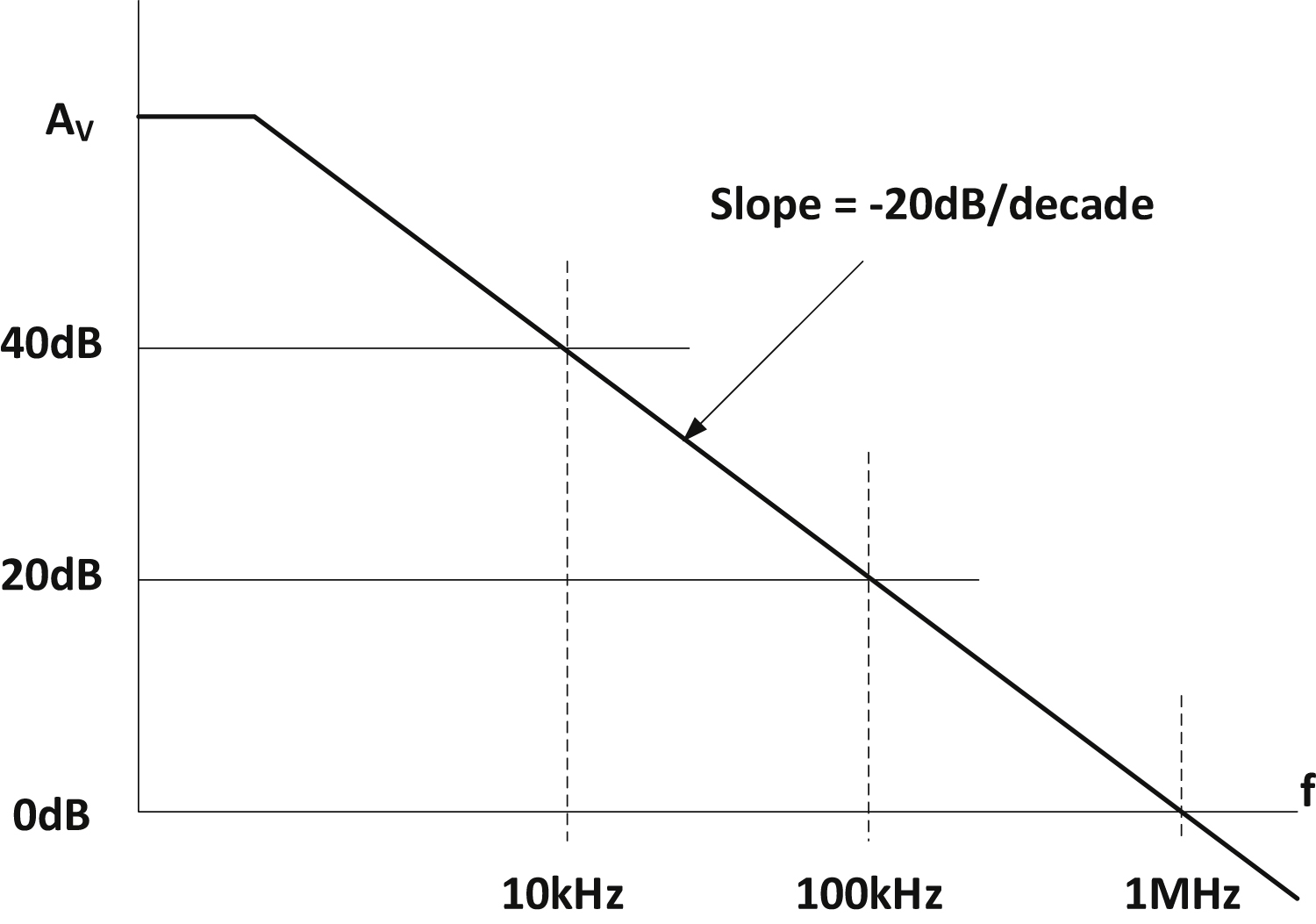
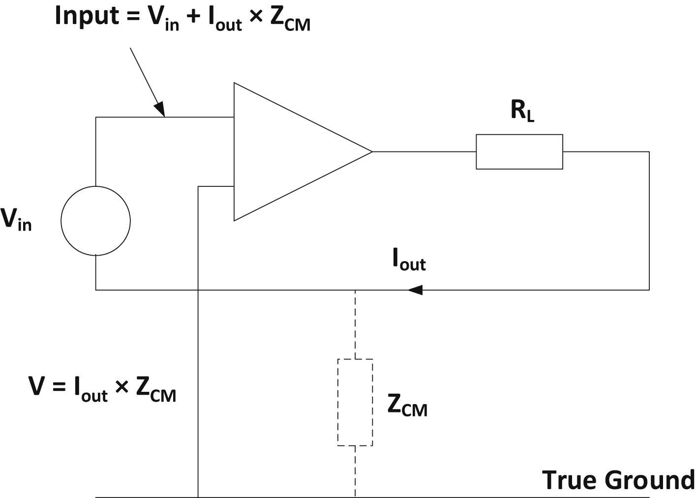


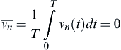 (5.6)
(5.6)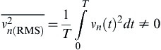 (5.7)
(5.7)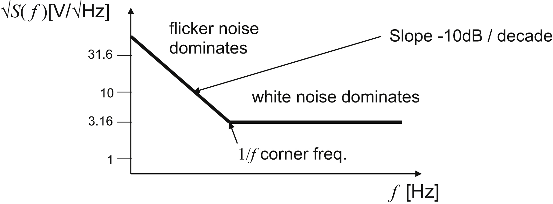

 (5.12)
 (5.13)
 (5.15)
 (5.16)
 (5.17)