Chapter 2
Printed Circuits
Abstract
Virtually every electronic circuit built nowadays uses a printed circuit board (pcb) as both its interconnecting medium and mechanical mounting substrate. The pcb is custom-designed for the circuit it carries, and its selection is an important part of the circuit designer's task, though this is frequently delegated to the (perceived) inferior function of pc layout draftsman. The design of the pcb has a strong effect on the mechanical and electrical performance of the final product. This chapter looks at the main factors that you should consider when working with your new pcb design.
Keywords
Copper cladding; Fiberglass; Ground plane; Packing density; Printed circuit board; Reliability and maintainability
Virtually every electronic circuit built nowadays uses a printed circuit board (pcb) as both its interconnecting medium and mechanical mounting substrate. The pcb is custom-designed for the circuit it carries, and its selection is an important part of the circuit designer's task, though this is frequently delegated to the (perceived) inferior function of pc layout draftsman. The design of the pcb has a strong effect on the mechanical and electrical performance of the final product. This chapter looks at the main factors that you should consider when working with your new pcb design.
2.1. Board Types
An unprocessed board is a laminate of a conductive material and an insulating dielectric substrate. The different materials that are used, and the different ways of laminating and interconnecting between conductive layers, decide the type.
2.1.1. Materials
The conductive layer is almost invariably copper foil, adhesive bonded under heat and pressure to the substrate. The copper cladding thickness is usually specified (for historical reasons) by its weight per square foot, the most common being 1 or 2 oz, other thicknesses being 0.25, 0.5, 3, and 4 oz. Thickness of 1-oz copper is typically 0.035 ± 0.002 mm, other weights being thicker or thinner pro rata. The main deciding factor in choosing copper weight is its resistivity. Fig. 2.3 gives resistance versus track width for the different weights.
The most common laminates are epoxy glass and phenolic paper. Phenolic paper (or synthetic resin–bonded paper) is cheaper and can be punched readily, so its major application is in high-volume domestic and other noncritical sectors. It is electrically inferior to epoxy glass, is mechanically brittle, has a poor temperature range, absorbs moisture readily, and is unsuitable for plated-through-hole (PTH) construction. You will only find it used for very cost-sensitive, low-performance applications. Otherwise, epoxy glass is universal except for specialist applications such as RF circuits.
Epoxy Glass
Epoxy resin with woven glass cloth reinforcement is used for PTH and multilayer boards. It can also be used for simpler constructions if its better mechanical and electrical properties are needed. It offers much better dimensional stability and is stronger than phenolic paper, but this does mean that high-volume boards cost more because it must be drilled rather than punched. For even denser and more dimensionally critical boards, epoxy aramid is another suitable material. Table 2.1 gives a selection of material specifications for some frequently used types of board material. The common designation of “FR4” refers to the American National Electrical Manufacturers' Association (NEMA) specification for flame-retardant epoxy-woven glass board, which is offered by most laminate manufacturers; there are many flavors of FR4, having better or worse specifications but all of them meeting the NEMA requirements. Flame-retardant grades are available for all common materials and are shown by the manufacturers' ID being marked in red.
For flexible boards the base films are polyester or polyimide. Polyester is cheap but cannot easily be soldered because of its low softening temperature so is used primarily for flexible “tails.” Polyimide is more expensive but components can be mounted on it.
Table 2.1
Printed Circuit Board Laminate Material Properties
| Material | Surface Resistance (MΩ) | Dielectric εr | Dielectric tan δ | Dielectric Strength (kV/mil) | Tempco x–y (ppm/°C) | Maximum Temperature (°C) |
| Standard FR4 | Minimum 1.104 | Maximum 5.4, typical 4.6–4.9 | Maximum 0.035 | 1.0 min | 13–16 | 110–150 |
| FR408 (high quality) | 1.106 | 3.8 | 0.01 | 1.4 | 13 | 180 |
| Epoxy aramid (close tolerance) | 5.106 | 3.8 | 0.022 | 1.6 | 10 | 180 |
| Polyimide (Kapton) | – | 3.4 | 0.01 | 3.8 | 20 | 300 |
| Polyester (Mylar) | – | 3.0 | 0.018 | 3.4 | 27 | 105 |

2.1.2. Type of Construction
Most circuit requirements can be accommodated on one of the following board types, which are listed roughly by increasing cost.


1. Single-sided
Cheap and cheerful for simple, low-performance and/or high-volume circuits (Fig. 2.1).
2. Double-sided
As above, but different track pattern on each side of the board, through connections made on assembly, e.g., low-density applications (Fig. 2.2).
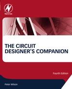
3. Flexible
Base material thin and flexible, may be covered with further layers to protect track pattern. May be through-hole plated. Replacement for wiring harnesses (Fig. 2.3).
4. Double-sided PTH
Similar to ordinary double-sided but hole barrels are metal plated to interconnect both sides, so a different production technique. Medium density general industrial etc. applications (Fig. 2.4).
5. Rigidized Flexible
As flexible, but part stiffened by rigid plate for component mounting. Used where application requires few components with flexibility (Fig. 2.5).
6. Multilayer
Several layers of base material laminated into a single unit. Variants may have holes passing through all layers or only internal layers (buried vias). Internal layer pairs may be power and ground planes. Expensive, but very high densities achievable with many layers. See Section 2.1.5 (Fig. 2.6).
7. Flexi-rigid
Multilayer boards with some rigid layers replaced by flexible areas (usually polyimide), which extend away from the rigid section to form tails or hinges. Several rigid areas may be interconnected by flexible areas to allow folded shapes for dense packing (Fig. 2.7).
Many variants of the basic multilayer and flexi-rigid principles are possible, for instance, up to 24 layers can be fabricated in the multilayer construction (see Section 2.1.5). Other techniques and materials are available for specialized functions such as switch contacts, motor assemblies, or microwave systems. If you have these kinds of applications, you will be talking to pcb manufacturers at the concept stage. But, if your application is more typical, how do you select the best approach?
2.1.3. Choice of Type
As in any design problem, many factors need to be balanced to achieve the best final result. The most important are cost, packing density, and electrical performance, with other factors appearing to a lesser extent.
• Cost. The above list gives an idea of ranking in terms of bare board cost, though there will be a degree of overlap. The actual cost formula involves board quantity ordered, number of processes, number and variety of drill holes, and the raw material cost as its main parameters. But as well as bare board cost you should also consider the possible effect on overall unit costs; the choice of board type can affect assembly, test, repair, and rework. For instance, if you expect to rework a significant number of units, this would rule out phenolic paper because of its poorer copper-laminate adhesion. At the other extreme, it could work against multilayer boards because of the danger of destroying an otherwise good board by damaging one through hole.
• Space limitations. If your board size is fixed and so is your circuit package count, then you have automatically determined packing density and to a great extent the optimum board type for lowest cost. Non-PTH boards give the lowest packing density. Double-sided PTH can offer between 4 and 7 cm2 per 16-pin dual-in-line (DIL) through hole package depending on track spacing and dimensions, while multilayers can approach the practical limit of 2 cm2 per pack. Multilayers are also the only way to fully realize the space advantages of flat-pack or surface-mount components. Large, discrete-leaded components (resistors, capacitors, transformers, etc.) reduce the advantage of multilayers because they effectively offer more area for tracking on the surface. If there is no limitation on board size, then using a larger, cheaper, low-density board must be balanced against the cost of its larger housing.
• Electrical characteristics. Phenolic paper may not have sufficiently high bulk resistance, voltage breakdown, or low dielectric loss; or the laminate thickness may be determined by required track characteristics, although usually it's easier to work the other way round; or thicker copper may be required for low resistivity. If surface leakage is likely to be a problem, conformal coating is one solution (see Section 2.4.1). For proper power/ground plane distribution, a minimum four-layer multilayer construction is normal; for lower densities the ground plane can be put on one side of a double-sided board.
• Mechanical characteristics. Weight, stiffness, and strength may all be important. If you need good resistance to vibration or bowing, either a thicker laminate or stiffening bars may be required. Usually, strength is not critical unless the board carries very heavy components such as a large transformer, in which case epoxy glass is essential. Coefficient of thermal expansion and maximum temperature rating may need checking if you have a wide-temperature range application.
• Availability. Just about any pcb manufacturer should be able to cope with ordinary single-sided and double-sided and PTH boards, though prices can vary widely. As you progress toward the more exotic flexible and multilayer constructions your options will diminish and you could become locked in to a single source or face unacceptable delivery times. Also, designing complex multilayer boards requires an advanced level of skill, even with improving CAD systems, and your design resources may not cover this when faced with short timescales.
• Reliability and maintainability. These factors normally favor uncomplicated construction with high-quality materials, for which double-sided PTH on epoxy glass wins out easily.
• Rigid versus flexi. The flexi-rigid construction may offer lower assembly costs and better packing density and reliability by eliminating interboard wiring and connectors. Against this it is more expensive and more prone to difficulties in supply and may run counter to a repair philosophy based on modular replacement.
2.1.4. Choice of Size
If you have a free hand in selecting the size of the board or boards in your system, then another set of factors need to be considered. It may be best to go for a standard size such as Eurocard (100 × 160 mm) or double-Eurocard (233.4 × 160 mm) especially if the boards will be fitted into a modular rack system. Modularizing the total system like this may not be optimum, though; for smaller systems a single large board will do away with the cost of interconnecting components and will be cheaper to produce than several smaller boards of equivalent area. On the other hand, board material costs depend to some extent on wastage in cutting from the stock laminate, and larger boards are likely to waste more unless their dimensions are matched to the stock. Also, there is a practical limit to the size of very large boards, fixed by considerations of stiffness, dimensional tolerancing and handling, not to mention the capability of the board manufacturer, photoplotter, and layout generation. Your own assembly department will also have limits on the board size they can handle. Optimum size for large boards is generally around 30–50 cm on the longer edge.
With the advent of modern production techniques and the concept of multiple panels, many companies now offer a cheaper service where many boards are produced in a single process, thus sharing the tooling costs. This “pooling” service can make it cost-effective to go for much smaller board sizes, even when prototyping or for small quantities—more on this in the section on panelization.
Subdivision Boundaries
If you are going to split the system into several smaller boards, then position the splits to minimize the number of interconnections. Often this corresponds with splitting it into functional subassemblies, and this helps because it is easiest to test each assembled board as a fully functioning subunit. Test cost per overall system will decrease as the board size increases, but the expense of the required automatic test equipment will rise. Allow a safety factor in your calculations of the board area needed for each subsystem: subsequent circuit modifications nearly always increase component count, and very rarely reduce it.
Panelization
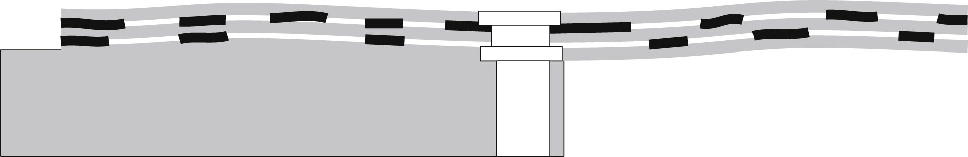
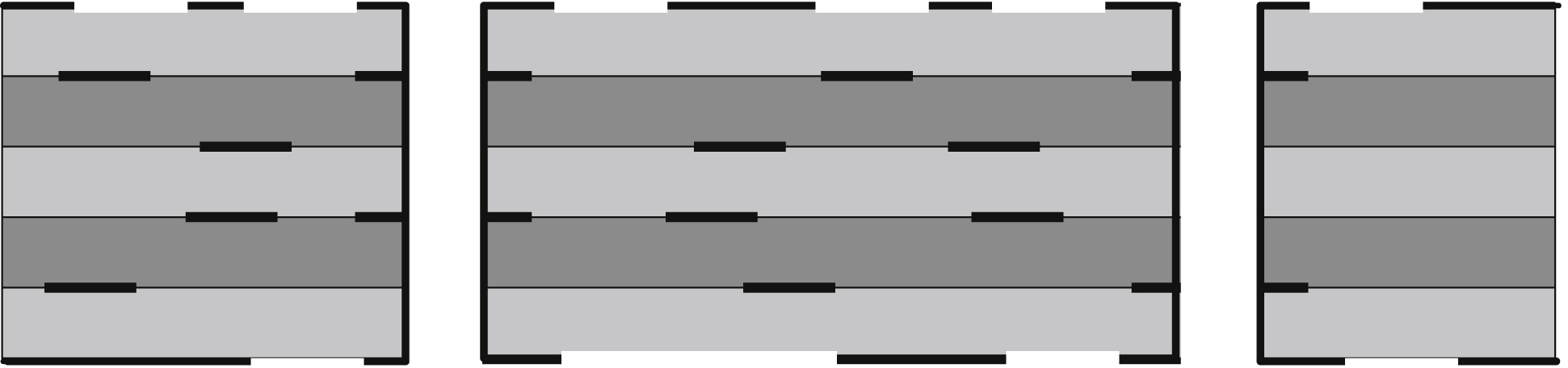
It is unusual for smaller boards to be built one per stock laminate. In a production run, the main cost is in the processing stages, and if, say, half a dozen boards can be made at a time in one piece the processing and handling applies simultaneously to all of them as if they were one board. The artwork for one board is simply repeated in steps across the whole panel (Fig. 2.8). At the end of the processing—quite probably even after delivery, population and assembly of components—they can be separated. They do not even have to be the same design, as long as they have identical layer stack-ups. You may, for instance, want to put all the boards for one project into one panel, since the numbers required for each will be identical.
The size of the board can then be matched to a multiple of a given stock size, allowing for routing and/or score lines to give separation. It can also be cost-effective if you have a board with a large waste area, for instance, a thin L-shape, to put other boards into the waste region and make use of it. Although panelization reduces your options in some respects, because all the boards on a given panel must have the same layer count and thickness, it is worth accepting these limitations for the sake of greater cost-effectiveness.
2.1.5. How a Multilayer Board is Made
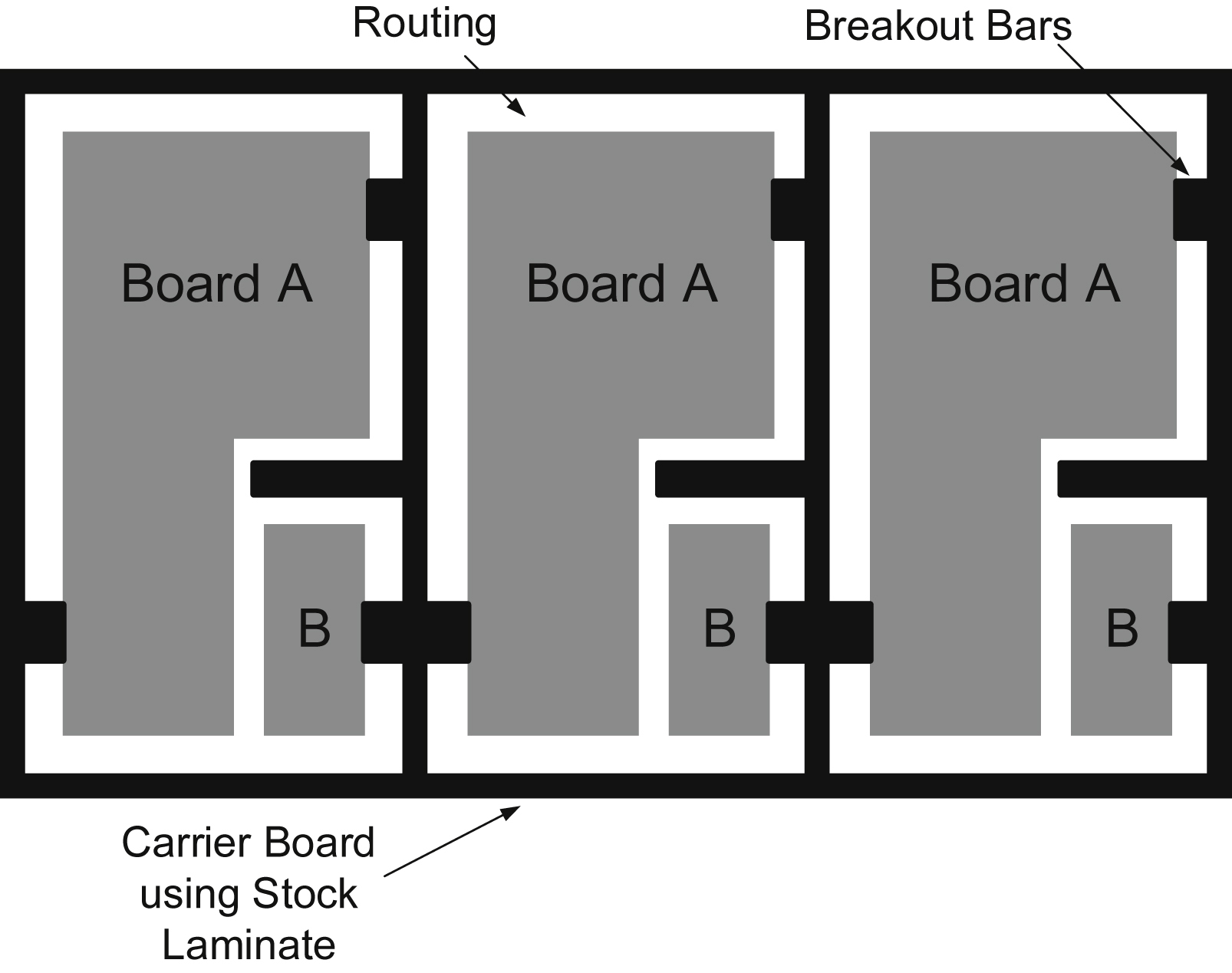
The stages of processing for a multilayer board are well established (Fig. 2.9–2.16 shows the process of making a six-layer board as an example). The finished board consists of a sandwich (Fig. 2.9) of double-sided copper inner layer pairs—each one processed and etched separately with its track patterns—which are separated by layers of “prepreg,” plain epoxy-glass material without copper laminate. The outer copper layers are applied as foil, initially unprocessed. Because of this method of assembly, multilayer boards always consist of an even number of copper layers—four, six, eight, and so on.
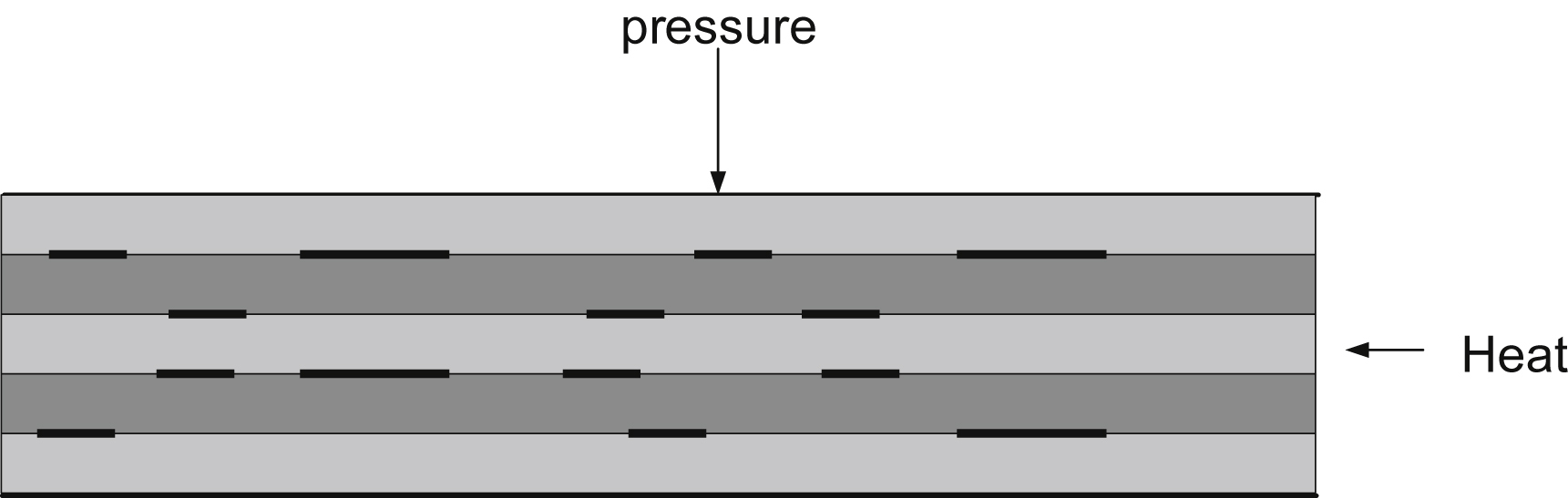

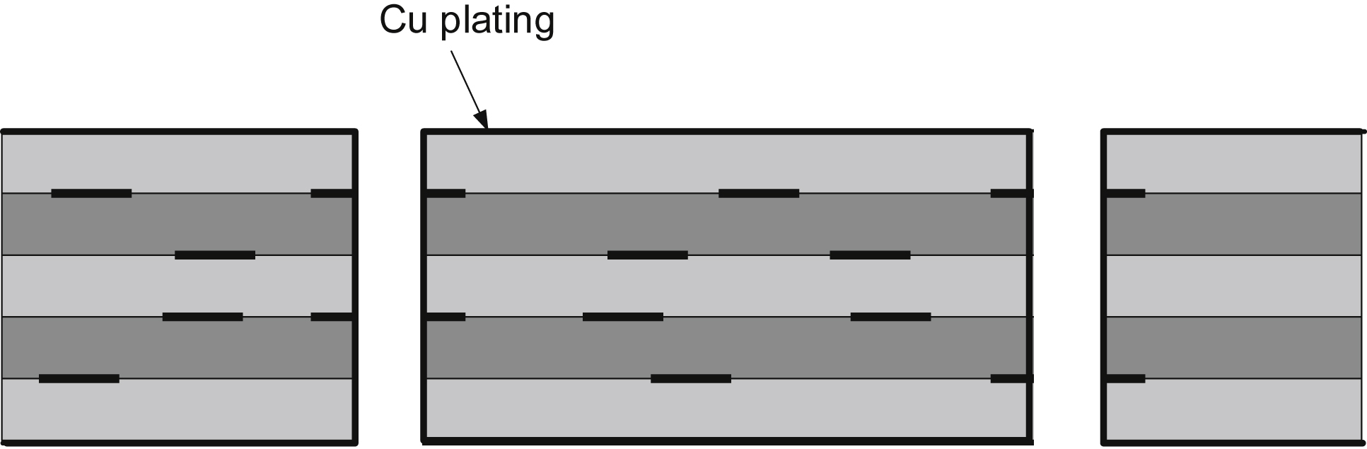

The individual sets of inner layers, prepregs, and outer foil are bonded together (Fig. 2.10) under heat and pressure. The alignment tolerances between the layers have to be established at this step. The assembly is then drilled according to the required pattern (Fig. 2.11). The holes may be used for vias, in which case they will only interconnect different layers, or for component lead wires, or for other purposes such as mounting the final assembly. After this, the whole assembly is put through a copper plating process (Fig. 2.12), which adds copper to all exposed surfaces: through the barrel of each hole (hence the designation “plated-through-hole”) and also on the surface of the copper foil on each side. The vias are created at this step by the contact of the hole plating with the edges of the appropriate pads on the inner layers.
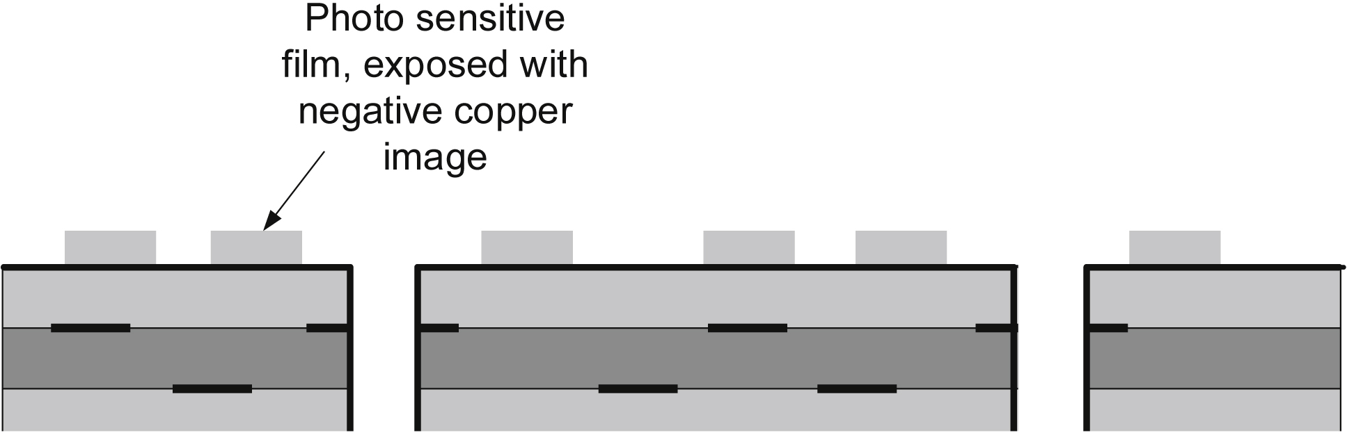
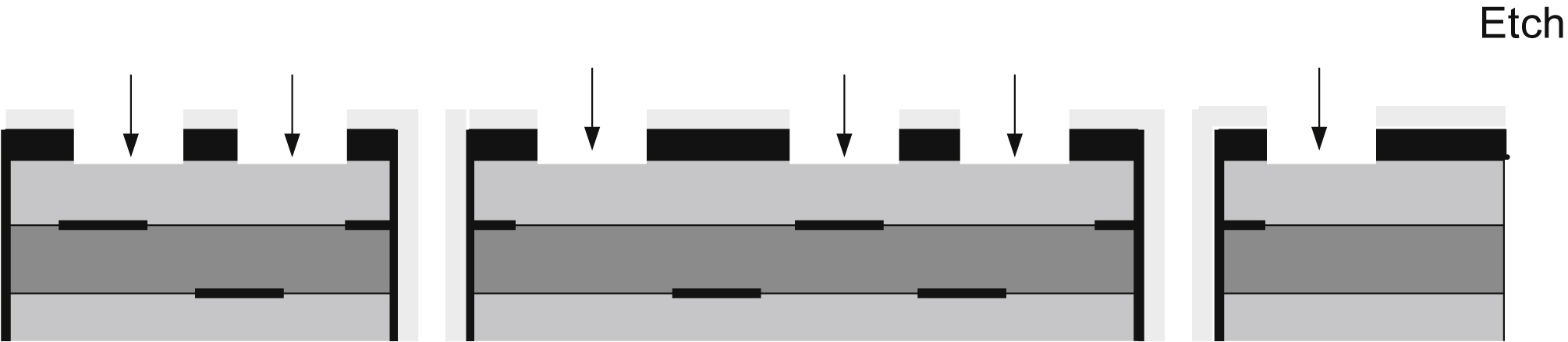
The two outside layers are then processed by applying a photosensitive film, and then exposing and developing this (Fig. 2.13) to leave a negative image of the required outer track and pad pattern. Further plating (Fig. 2.14) adds more copper and a protective tin coat to the exposed areas; the photosensitive film is removed, and the board is etched (Fig. 2.15) to take off the copper that was underneath it. The tin is then stripped away leaving the complete three-dimensional copper pattern outside and within the board (Fig. 2.16), ready for the application of solder mask and surface finishing. The thickness of the outer copper layers is the sum of the total plating thickness and the initial foil thickness.
2.2. Design Rules
Most firms that use pcbs have evolved a set of design rules for layout that have two aims:
• ease of manufacture of the bare board, which translates into lower cost and better reliability;
• ease of assembly, test, inspection, and repair of the finished unit, which translates as above.
These rules are necessary to ensure that layout designers know the limits within which they can work, and so that some uniformity of purchasing policy is possible. It has the advantage that the production and servicing departments are faced with a reasonably consistent series of designs emanating from the design department, so that investment in production equipment and training is efficiently used. At the same time, the rules should be reviewed regularly to make sure that they do not unnecessarily restrict design freedom in the light of board production technology advances. Any company, for instance, whose design rules still specify minimum track widths of 0.3 mm is not going to achieve the best available packing densities. The design rules should not be enforced so rigorously that they actually prevent the optimum design of a new product.
BS6221 Part 3, “Guide for the design and use of printed wiring boards,” presents a good overview of recommended design practices in pc layout and can be used to form the basis of in-house design rules.
Factors in board design that should be considered in the design rules are as follows:
• track width and spacing
• hole and pad diameter
• track routing
• ground distribution
• solder mask, component identification, and surface finish
• terminations and connections
Typical capabilities for pcb producers at the time of writing are shown in Table 2.2. Having decided on a particular supplier, the first thing you should be clear about is their capabilities in these key areas.
2.2.1. Track Width and Spacing
The minimum width and spacing determine to a large extent the achievable packing density of a board layout. Minimum width for tracks that do not carry large currents is set by the controllability of the etching process and layer registration for multilayers, which may vary between board manufacturers and will also, at the margins, affect the cost of the board. You will need to check with your board supplier what minimum width he or she is capable of processing. Table 2.2 suggests typical capabilities in this respect at the time of writing, for 1-oz thick copper; thicker copper will demand greater widths because of undercutting in the etching. The narrowest widths may be acceptable in isolated instances, such as between IC pads, but are harder to maintain over long distances. Fig. 2.17 shows the trade-off in track width and spacing versus number of tracks that can be squeezed between IC pads.
Table 2.2
Typical Best Capabilities of Printed Circuit Board Manufacturers
| Board thickness range | 0.35–3.5 mm |
| Maximum number of layers | 14–24 |
| Minimum track and gap width (1-oz copper) | 0.1 mm possible, 0.15 mm preferred |
| Minimum PTH diameter | 0.2 mm possible, 0.3 mm preferred |
| Maximum PTH aspect ratio | 12:1 possible, 6:1 preferred |
| Registration: Drill to pad | 0.03 mm |
| Registration: Layer to layer, including solder mask | 0.075 mm |
Conductor Resistance
Track width also, rather more obviously, affects resistance and hence voltage drop for a given current. Eq. (2.1) shows the theoretical resistance for various thicknesses of copper track per centimeter. It is derived from Eq. (2.1):
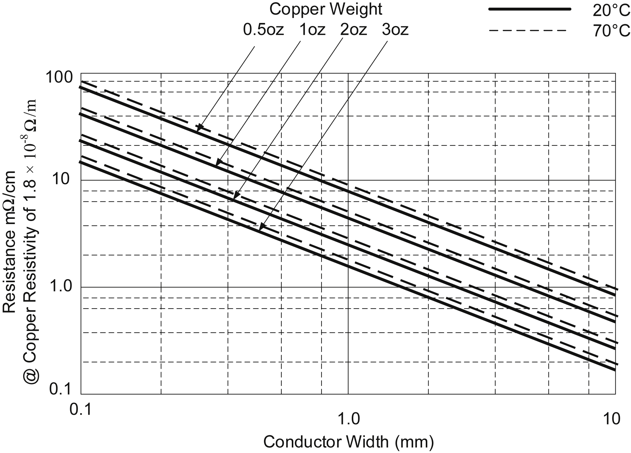

These figures should only be taken as a guide because the actual manufactured tolerances, including base copper, plating and tin–lead thickness, will be very wide, amounting to a two-to-one variation in final value. The temperature coefficient of copper means that resistance will vary by several percent over typical ambient temperature ranges, and with self-heating. PTHs of greater than 0.8 mm diameter present less than a milliohm resistance.
The maximum current-carrying ability is determined by self-heating of the tracks. Fig. 2.18 shows the safe current versus track width for a given temperature rise.
Voltage Breakdown and Cross Talk
Track spacing is also determined by production capability and electrical considerations. Minimum spacings similar to track widths as shown in Table 2.2 are achievable by most pcb manufacturers. Cross talk and voltage breakdown are the electrical characteristics, which affect spacing. For a benign environment—dry and free from conductive particles—a spacing of 1 mm per 200 V, allowing for manufacturing tolerances, is adequate for preventing breakdown. BS6221 part three gives greater detail. When mains voltages are present, wider spacing is normally set by safety approval requirements. Spacings less than 0.5 mm risk solder bridging during wave soldering, depending on the transport direction, if solder resist is not used.
Cross talk (see Section 1.2.7) is likely to be the limiting factor on low-voltage digital or high-speed analogue boards. The mechanism is similar to that for cables; calculating track-to-track capacitance is best performed by electromagnetic field solvers for individual tracks working on the actual board layout. The simplest rule of thumb is that a track spacing greater than 1 mm will result in cross talk voltages less than 10% of signal voltages for most board configurations. Electrically short connections can be spaced much closer than this without undue concern. Cross talk can be reduced by routing ground conductors between pairs of signal lines considered susceptible.
Constant Impedance
For high frequency, longer tracks, including those that carry fast digital signals, it is necessary to design the conductors as a transmission line. The basic idea behind transmission line propagation is covered in Section 1.2.8; the important principle is that a signal conductor and its return path are considered as a whole and designed for a specific characteristic impedance (Z0). Z0 is a function of the geometry of the line and the relative permittivity of the material, which encloses it. Clearly these two factors are specific to each pcb design and construction. This means that, if you are going to have to rely on transmission lines in the circuit, you will have to designate certain layers as “constant impedance” layers.
It is usual, though not universal, to use microstrip construction (Table 1.9) in which a signal track is routed against a ground plane, which is the return path, or (on the inner layers) stripline construction in which the track is sandwiched between two ground planes. The principal geometrical factors in determining Z0 are then the track width and its separation distance from the ground plane. Track width tolerance is controlled by the etching process, and so a wider track (which means a lower Z0) gives a closer tolerance. The layer separation depends on the pressure applied during layer bonding and on the thickness tolerance of the prepreg or laminate materials. A thinner separation again gives a lower Z0.
For transmission lines on the inner layers, Z0 also depends on the square root of the relative permittivity εr of the epoxy-glass material. If the line is carried on the surface layer, the dependence is more complicated because part of the dielectric (above the line) is air, while below the line it is epoxy glass. How tightly εr is controlled depends on the quality (and cost) of the base material. General-purpose FR4 does not have a tight specification on this parameter, although more premium materials are available specifically for the purpose of building constant impedance boards. Table 2.1 gives some details of typical materials.
2.2.2. Hole and Pad Size
The diameter for component mounting holes should be reasonably closely matched to the component lead diameter for good soldering, an allowance of 0.15–0.3 mm greater than the lead diameter giving the best results. Automatic insertion machines may require larger allowances. There is a trade-off between the number of differently sized holes and board cost, so it is not advisable to specify different hole diameters for each different lead diameter. Typically you will use 0.8 mm diameter for DIL package leads and most small components, 1.0 mm for larger components and other sizes as required. Remember to specify hole diameters after plating on PTH boards. Also, remember to double check component lead diameters against individual holes, when you are writing up the board specification—or, if your CAD system marks up hole diameters for you, make sure its component library is up-to-date. Some capacitors and power rectifier diodes in particular have larger leads than you may think! It is embarrassing to have to tell your production department to drill out holes on a double-sided PTH board, and then solder both sides because you got a lead diameter wrong. It is even more embarrassing if it's a multilayer board because you cannot drill out holes that connect to internal layers.
Vias
Via holes—PTHs that join tracks on different layers—can be any reasonable diameter, subject to current rating. The smallest useable diameter is linked to board thickness, and generally a ratio of thickness to diameter (aspect ratio) of up to 6:1 will not present too many problems in plating. But, unless you are forced into small diameter vias by constraints of packing density, you should keep them either equivalent to the smallest component hole diameter so that drill sizes are kept to a minimum or make them one size smaller (e.g., 0.6 mm) so that the likelihood of false insertion of component leads is low.
Through Hole Pads
Pads can be oval or round. Oval pads for DIL packages on a 0.1″ pitch are a hangover from early days in pcb technology when a large pad area was needed to assure a good soldered joint and good adhesion of the pad to the board. This is still advisable for non-PTH boards, and a typical round pad for a 0.8 mm diameter hole would be around 2 mm diameter, which leaves no room for tracking between pins. An oval allows one track between each pad. Some care is needed with oval pads as the hole-to-pad tolerance in the width dimension can be tight.
PTH technology reinforces the pad-to-board bond on both sides by the plating in the barrel of the hole, and the solder flows into the annulus between lead and hole plating, so that large or oval pads are unnecessary on PTH boards. The pad need only contain the drilled hole before plating, with allowance for all manufacturing tolerances. For a 0.8 mm diameter hole the pad diameter can be between 1.3 and 1.5 mm (Fig. 2.19).
Pads for larger holes on non-PTH boards should exceed the hole diameter by at least 1 mm to obtain good adhesion. The ratio of pad-to-hole diameter should be around 2 for epoxy glass and 2.5–3 for phenolic paper boards.
Surface Mount Pads
Pad sizes for SM components are determined by the individual component terminals and by the soldering technology used: wave or reflow (see Section 2.3.1). You have virtually no choice over these dimensions once you have chosen the assembly method and the component. CAD systems will all have libraries of the component and associated pad dimensions and will automatically layout the artwork for the correct sizes—provided, of course, that their libraries are correct. You may need to check this on occasion, and when you introduce a new component to the library you will need to be sure that you have incorporated the proper pad layout; component suppliers will normally include recommended pad dimensions in their datasheets.

2.2.3. Track Routing
The first rule of good routing is to minimize track length. Short tracks are less susceptible to interference and cross talk, have lower parasitic reactances, and radiate less. Routing should proceed interactively with package placement to achieve this. It is often possible to improve routing prospects when using multifunction packages (typically gates or op-amps) by swapping pins, so unless there are overriding circuit considerations you should not fix pinouts on these packages until the layout has been finalized. A good CAD package with an extensive and intelligent component library will do this automatically. Similarly, you may have decided on grounds of package economy to use up all the functions in a package, but this could be at the expense of forcing long tracks to one or other function. An optimum board layout may require a few more packages than the minimum.
Many CAD autorouting software packages will lay all tracks of one orientation on one layer of the board and all of the other orientation on another layer (X–Y routing). This works and is fast, especially for low-performance digital boards, but hardly ever produces an optimum layout in terms of minimum track length and number of via holes and can be disastrous on analogue boards. Normally you should anticipate expending some skilled design effort at the layout stage in cleaning up the CAD output to produce a cheaper board with better electrical performance.
45 degrees-angled bends are preferable to right angles, as they allow a slight increase in tracking density. Right angles and acute angles in tracks are best avoided as they provide opportunities for etchant traps and the subsequent risk of track corrosion. When two tracks meet at an acute angle the join should be filleted to prevent this. Tracks should not be run closer than 0.5 mm from the edge of the board.
From a mechanical point of view, the aim should be to balance the total coverage of copper on both sides of a double-sided board or on all layers of a multilayer. This guards against the risk of board warping due to differential strains, either because of thermal expansion in use or because of stress relief when the board is etched, and also assists plating.
2.2.4. Ground and Power Distribution
Much of what could be said here has already been said in Chapter 1. Layout of ground interconnections is as important on pcbs as it is between them. Common impedances should be avoided in critical parts of the circuit, but usually the best compromise is a ground “bus” for much of the circuit. This is perfectly acceptable at low frequencies, low gains, low currents, and high signal levels, where the magnitude of voltages developed along the ground rail are well below circuit operating voltages.
Fig. 2.20 shows resistance versus track width, and this can be used to calculate DC voltage drops where necessary. The inductance of ground and power connections becomes important when high frequency currents are being carried; the voltage drops now depend on rate of change of current.
Ground Rail Inductance
pc track inductance is primarily a function of length rather than width. The formula given in Section 1.2.1 shows that for wires, inductance depends directly on length but only logarithmically on width. pcb tracks in isolation follow the same law, but the inductance of a track on its own is often misleading as it will be modified by proximity to other tracks carrying return current. Fig. 2.20 shows the principle of magnetic field cancellation of two close tracks carrying equal but opposite currents.
This shows that the most effective way of reducing total power and ground inductance is to run the signal and return paths very close together. This maximizes their mutual inductance, and since the currents now oppose each other, the total inductance is reduced by the mutual inductance rather than increased. One way to achieve this is to run power and ground rails with identical geometry on opposite sides of the board. But, if a compromise is necessary, it is better to use the board space to produce the best ground system possible and control power rail noise by decoupling (see Section 6.1.4).

Gridded Ground Layout
Good low-inductance power and ground rails can be assured on double-sided and multilayer boards by either of two techniques: grid layout or an overall or partial ground plane. The former is really an approximation of the latter. For many purposes, particularly when the layout is a regular pattern of ICs, and if the power and ground lines are well decoupled, a grid can approach the performance of a ground plane. Certainly a well-designed grid will be more effective than a poorly designed ground plane. A grid allows you to minimize sections of common impedance and ensures that lengthy ground separations are interconnected by several current paths. It is not advisable for sensitive analogue layouts when you need control of ground return current paths. In any case, an ideal grid will be too restricting for the signal paths and some compromise will be needed.
The Ground Plane
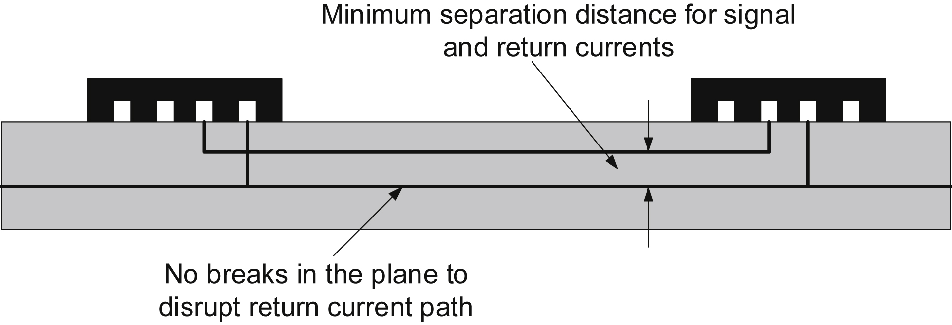
A ground plane scores when, as in analogue circuits or digital circuits with a mixture of package sizes, ground connections are made in a random rather than regular fashion across the layout. A ground plane is not necessarily, or even usually, created simply by filling all empty space with copper and connecting it to ground. Because its principal purpose is to allow the flow of return current (Fig. 2.21), there should be a minimum of interruptions to it, and for this reason ground planes are more successful on a multilayer board where an entire layer can be devoted, one to the power plane and one to the ground. This has the additional advantage of offering a low impedance between power and ground at high frequencies because of the distributed interplane capacitance.
Individual holes make no difference to the ground plane, but large slots (Fig. 2.22) do. When the ground plane is interrupted by other tracks or holes the normal low-inductance current flow is diverted round the obstacle and the inductance is effectively increased. Interruptions should only be tolerated if they do not cut across lines of high di/dt flow: that is, underneath tracks carrying high switching currents or fast logic edges. Even a very narrow track interconnecting two segments of ground plane is better than none. At high frequencies, and this includes digital logic edge transitions, current tends to follow the path that encloses the least magnetic flux, and this means that the ground plane return current will prefer to concentrate under its corresponding signal track.

Some board manufacturers do not recommend leaving large areas of copper because it may lead to board warping or crazing of the solder resist. If this is likely to be a problem, you can replace solid ground plane by a cross-hatched pattern without seriously degrading its effectiveness. To make a soldered connection to the ground plane—or any other large area of copper—on the surface of the board, you should “break out” the pad from the area and connect via one or more short lengths of narrow track (Fig. 2.23). This prevents the plane acting as a heat sink during soldering and makes for more reliable joints. This is not an issue for internal ground planes since the PTH increases the thermal resistance to the plane.

Inside or Outside Layers
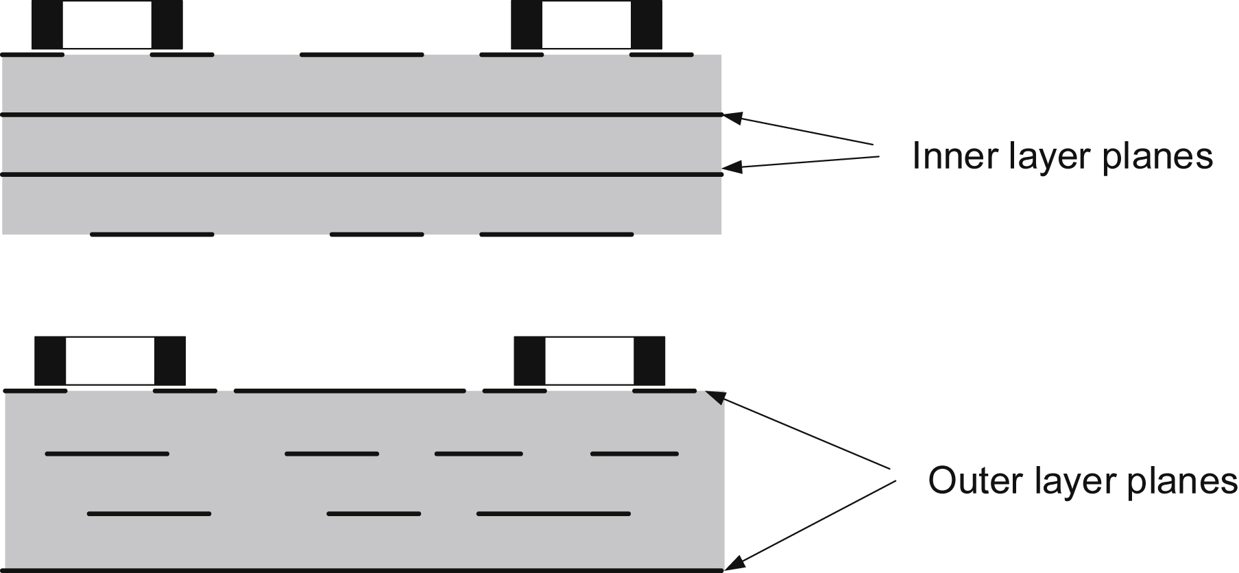
A common question is whether the power and ground planes should be put on the outer layers of a four-layer board or the inner layers. The situation is illustrated in Fig. 2.24. From the point of view of control of the current return path, the two approaches are largely equivalent: the return current in the plane is one layer away from its adjacent signal current whichever choice is made.
Putting the planes on the outside layers has the merit of providing an electric field screen for the tracks within. This might seem to be advantageous, but in fact as soon as you put components on the board then the screening is compromised; and the denser the component packing then the less use the screen is going to be, since there will be more area (the components, their leadouts, and their pads) outside the screen.
If two planes on the inner layers provide power and ground distribution, then putting them close together has the great advantage of giving a distributed, low inductance capacitance between them, which helps greatly with high frequency decoupling. It needs to be augmented with standard decoupling capacitor techniques, but the closer the planes are the better is the board's high frequency performance. Putting planes on the outside throws away this advantage entirely.
So a general rule would be if your board has few components but a lot of high frequency tracks, for instance, a system backplane, then by all means screen them with planes on the outside. But if the board has densely packed components that need good HF decoupling—which is probably 90% of designs—then the planes should go on the inside.
Multiple Ground Planes
There is no objection to, and a great deal of advantage from, having several layers devoted to notionally identical ground planes in a multilayer (say eight or above) construction. This allows each set of track layers to be placed next to a ground plane layer and minimizes the separation distance for each track layer through the board. It is necessary though either to be rigorous about preventing tracks from jumping layers from one ground plane to another, or more realistically, to “stitch” the planes together at frequent and short intervals with vias.
Separating ground planes in the x–y direction by providing “moats” around different segments of ground is much more problematical. Essentially, the problem is that as soon as you assign different ground segments, there will be some signals that have to cross the moat to get from one segment to another. These signals are then exposed to the full hostility of a compromised local return path. You should never do this if the signals are in any way critical (high frequency or low level) and, if they are not and you must, then treat each such signal with extreme care.
2.2.5. Copper Plating and Finishing
The surface of the conductors on the outside layers of a pcb needs to be finished, to allow component soldering, or connections, or protection against oxidation. The most common finishing for surface mount boards is hot air solder leveling, which applies a thin layer of solder and then blasts it with a hot air knife to make sure the surface will be flat enough to take the solder paste application for the chip components. But for other applications, it is also possible to specify gold, silver, or nickel plating, or carbon ink. Silver may be used for RF circuits to reduce the circuit losses; gold and nickel would typically be used for connector contacts. Carbon ink is a cheap and simple finish for keypad contacts, where the resistivity of the contact is unimportant, and it can also be used for low-specification resistors.
Each plating process is a separate operation and naturally increases the cost of the bare board, even before you add the cost of the plating material itself. The thickness of the plating can be varied from fractions of a μm to more than 10 μm and will depend on the performance required of the surface, for instance, whether there will be many reconnection operations or just a few. It is possible to mask areas of the board to prevent plating of that area, and it is also possible to add “peelable” masks over particular areas of plating to prevent their contamination by a wave soldering operation. For instance, gold-plated connector areas would end up coated with solder if they were passed unprotected through a solder bath, so the mask remains in place and is removed once the whole assembly process has been completed.
2.2.6. Solder Resist
Also known as solder mask, the solder resist is a thin, tough coating of insulating material applied to the board after all copper processing has been completed. Holes are left in the resist where pads are to be soldered. It serves to prevent the risk of short circuits between tracks and pads during soldering and subsequently, and it is also sometimes used as an anticorrosion coating and to provide a dark, uniform background for the component identification legend. It can be a screen-printed and oven-cured epoxy resin, a photographically exposed and developed dry film or a photo-cured liquid film.
Screen-Printed Resists
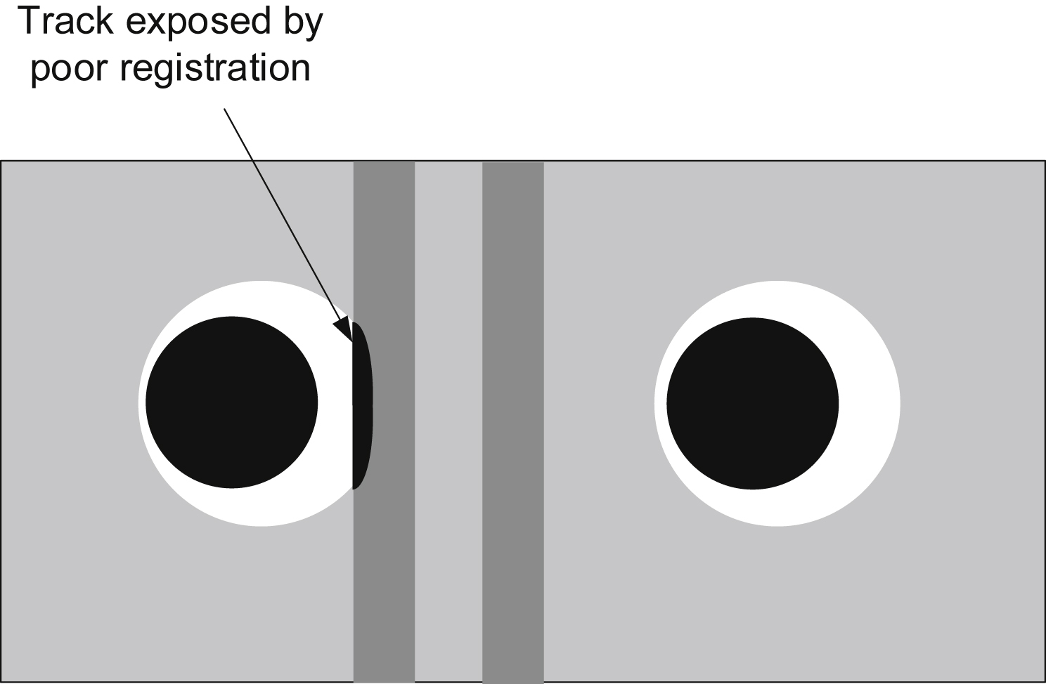
Screen-printed epoxy resin is a well-established method and is inexpensive, but achievable accuracies are poor compared to modern etching accuracies. The consequence of this is that there has to be an allowance for misregistration and resist bleeding of about 0.3–0.4 mm between the edges of pads and the edge of the solder resist pattern. It is easy to generate the artwork for this—simply repeat the pad pattern with oversize pads and generate a negative photographic image—but it cuts into the spacing between pads, and if fine tracks are run between pads, they may not be completely covered by the resist. Fig. 2.25 shows this effect. This nullifies the supposed purpose of the resist, to prevent bridges between pads and adjacent tracks! Also, screen-printed resists over large areas of copper that has been finished with tin–lead plating may crack when the board is wave soldered, as the plating melts and reflows. This is unsightly but not normally dangerous, as long as you do not rely on the resist as the only corrosion barrier.
Photo-Imaged Film
Photo film resists are capable of much higher registration accuracy and resolution (typically better than 0.1 mm) and are therefore preferred for high-density boards. They have their own problems, apart from expense, the main one being that dry films suffer lack of adhesion to poorly prepared board surfaces; liquid films have become the usual method as a result.
A solder resist should not always be regarded as essential (although for dense, wave-soldered surface mount boards, it is). It can be useful in reducing the risk of board failure through surface contamination or solder bridges but is not infallible. There is a danger that it is specified without thought or used as a crutch to overcome bad soldering practices. A well-designed board in a good production environment may be able to do without it.

2.2.7. Terminations and Connections
Any pcb that is part of a system must have connections to it. In the simplest case this is a wire soldered to a pad. If the board is plated-through, then this approach is acceptable, as the combined strength of solder in the plated hole plus the pad lands on both sides will be enough to cope with any normal wire flexing. Wires should not be soldered straight to non-PTH boards because the wire strains will be taken by the pad-to-board bond, which will quickly fail. Greater mechanical strength is needed.
This can be offered by feeding the wire back through a second hole in the board to give a measure of strain relief. Alternatively, use staked pins or “fish-beads.” A pin press-fitted into a hole transmits all mechanical strains directly into the board laminate, so the reliability of the pad-to-track transition is unaffected. Wire dressing to the pin is slightly more labor-intensive, but this is not usually a disadvantage. Fish-beads are easier to use but more expensive than pins; and because they are not staked to the board, they can transmit some strain to the pad. Both types are eminently suitable for individual test points. Fig. 2.26 shows the options.
Direct wire connections should not be dismissed out of hand because they are, after all, cheap. But as soon as several connections must be taken to the board, or repetitive disconnection is required, you will automatically expect to use a multiway pcb connector. This can take one of two forms, a two-part molded male/female system or an “edge” connector.
Two-Part Connectors
There are many standard pcb connectors available, and it is impossible to do justice to all of them. Popular ones are the DIN-41612 range for Eurocard-sized module boards, the many variants of square-pin stacked connectors pioneered by Molex and available from several sources in pin pitches from 0.05″ to 0.2″, the insulation displacement types with pc-mounting headers and free sockets, and the subminiature “D” range to MIL-C-24308 for external data links. All you can do is to compare data sheets from several manufacturers to find the best overall fit for your particular requirement. In connectors it is especially true that you get what you pay for in terms of quality.
Contact resistance will be important if the connector carries appreciable current, as will be the case for power supply rails. Even more important is whether a low contact resistance will be maintained over time in the face of corrosion and repeated mating cycles. This depends mainly on the thickness of gold plating on the mating surfaces. A wise precaution is to dedicate several ways of a multiway connector in parallel for each power and ground rail, to guard against the effects of increasing contact resistance and faulty pins.
Insertion and withdrawal force specifications tend to be overlooked, but serious damage to a board can result if too much force has to be used to plug it in. Conversely, if the withdrawal force is low and/or the plug–socket pair is not latched, there is the risk of the connectors falling apart or vibrating loose. As with single wires, it is better to provide a separate route for diverting the mechanical strain of the interconnection into the board laminate rather than relying on the solder joints to individual pins. Connector moldings that allow for nut-and-bolt fixing are best in this respect. Incidentally, remember to specify on the production drawing that fixings should be tightened before the pins are soldered—otherwise strain will be put on all the soldered joints as soon as the nuts are torqued up, resulting in unreliable connections later.
Edge Connectors
Edge connector systems are popular with many designers because they are relatively cheap. In this case, the connector “finger” pattern is part of the pcb layout at the board edge, and the board itself plugs into a single-piece female receptacle on the mating part. The board should have a machined or punched slot at some point in the pattern, which mates with a blanking key in the receptacle, to ensure that the assembly is plugged in the right way round and to align the individual connectors. The ends of the receptacle can then be left open. This is safer than aligning the board edge with the end of a closed receptacle, as it is more accurate and less susceptible to damage.
The fingers on the board must be protected from corrosion by gold plating. The plating should cover the sides as well as the tops of the fingers, otherwise long-term corrosion from the edges will be a problem. Pay attention to dimensional tolerancing of the pcb, both on board thickness to ensure correct contact pressure and on machining to ensure accurate mating. A useful trick if you have spare edge connector contacts is to run them to a dummy pad in some unused space inboard. They will prove invaluable when you discover a need for more connections during prototype testing!
One final point on pcb connectors is to make sure that your chosen connector type and board technology are compatible. Very high-density connectors are available, which have multiple rows of pins at less than 0.1″ spacing. These require very fine tracking to get between the outer rows to the inner ones. Also, they are a nightmare to assemble to the board, and you may find that your production department wants larger holes than you bargained for, which makes the tracks even finer. Do not go for high-density connectors unless you really have to: stick with the chunky ones.
2.3. Board Assembly: Surface Mount and Through Hole
There are two ways of mounting components to the board:
• surface mount, in which the surface mount devices (SMDs) have termination areas rather than leads and are held in place only by solder between pads on the board and their terminations
• through hole, in which the components have lead wires, which are taken through holes in the board. Such components are larger, and the net result is a considerably lower component density per unit area.
These are compared in Fig. 2.27. Because of its advantages, surface mount technology (SMT) makes up around 90% of board assemblies, but through hole still accounts for the remainder and is unlikely to disappear completely.
The advantages and disadvantages of SM construction versus through hole can be summarized as follows:
Advantages
• Size. Very much higher packing densities can be achieved. Components can be mounted on both sides if necessary. Enables applications that would be impossible with through hole.
• Automation. SM component placement and processing lends itself to fully automated assembly and so it is well suited to high-volume production. Unit assembly costs can be lowered.
• Electrical performance. Reduced size leads to higher circuit speeds and/or lower interference susceptibility. Higher performance circuits can be built in smaller packages—a prime marketing requirement.
Disadvantages
• Investment. To properly realize the potential of automated production, a sizeable capital investment in machinery is needed. This is normally measured in hundreds of thousands of pounds.

• Components. Most component types are available as SMDs, but still there are specialized types, which are only obtainable as through-hole mounting. Higher-power and large components can never be surface mounted.
• Criticality of mechanical parameters. Traditionally, any electrically equivalent component would do if it fitted the footprint. With SM, mechanical equivalence is as critical as electrical equivalence because the placement and soldering processes are that much less forgiving. This leads either to unreliability or to difficulties with component sourcing. Also, solderability and component shelf life become dominant issues.
• Test, repair, and rework. It is possible to test and rework faulty SM boards, with tweezers, a hot air gun, and a magnifying glass. It is a lot easier to test and rework through hole boards. Be prepared for extra expense and training at the back end of the production line.
The investment that is needed for a company that is contemplating doing its own SM production extends beyond simply acquiring the production equipment. There is probably an equivalent investment in CAD design tools, storage and procurement systems (to cut down component shelf life), test equipment, and rework stations, plus a hefty amount of time for retraining. Many companies will therefore prefer to use the services of a subcontract assembly house, despite a loss in their own profit margin, if their product volume cannot justify this investment. An important benefit of this approach is that it allows a firm to experiment with SMT, and gain some market and product experience with it, before full commitment. The other side of the coin is that the production staff do not gain any significant experience.
The stages of design, assembly, and test are very much more tightly coupled in SM than they need to be in conventional manufacture. The successful production and testing of an assembly is critically related to the pcb layout and design rules employed.
2.3.1. Surface Mount Design Rules
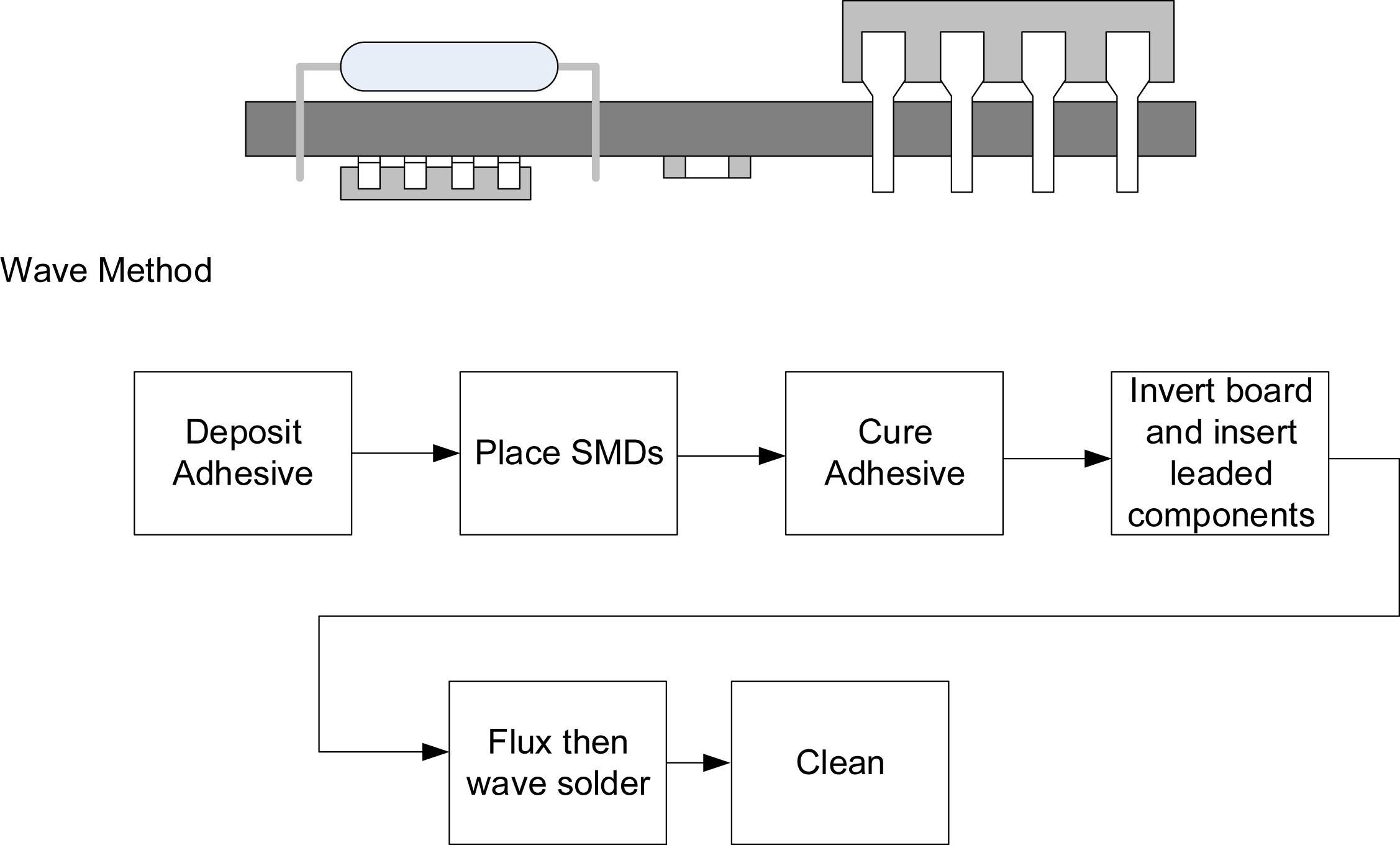
Pad dimensions and spacing are relative to the component body and leadouts and depend on the soldering method that will be used with the board. Components can either be placed over a dot of adhesive to hold them in place and then run through a wave soldering operation or they can be placed on a board, which has had solder paste screen printed onto the pads, in which case the tackiness of the solder paste holds them lightly in position until it is reflowed, either by an infrared oven or a hot vapor bath. Fig. 2.28–2.31 shows the different stages for each type of production.
Solder Process
If the board will be wave soldered, then the IC packages should be oriented along the direction of board travel, across the wave, and a minimum spacing should be observed. This optimizes solder pickup and joint quality. Pad dimensions need to be fairly large to take up placement tolerances, since the absolute position of the package cannot be altered once the adhesive is cured. The advantage of wave soldering is that it can simultaneously process surface mount and conventional components, if they are mounted on opposite sides. The maximum height of the SM components will be determined by the risk of being detached from the board when passing through the wave.

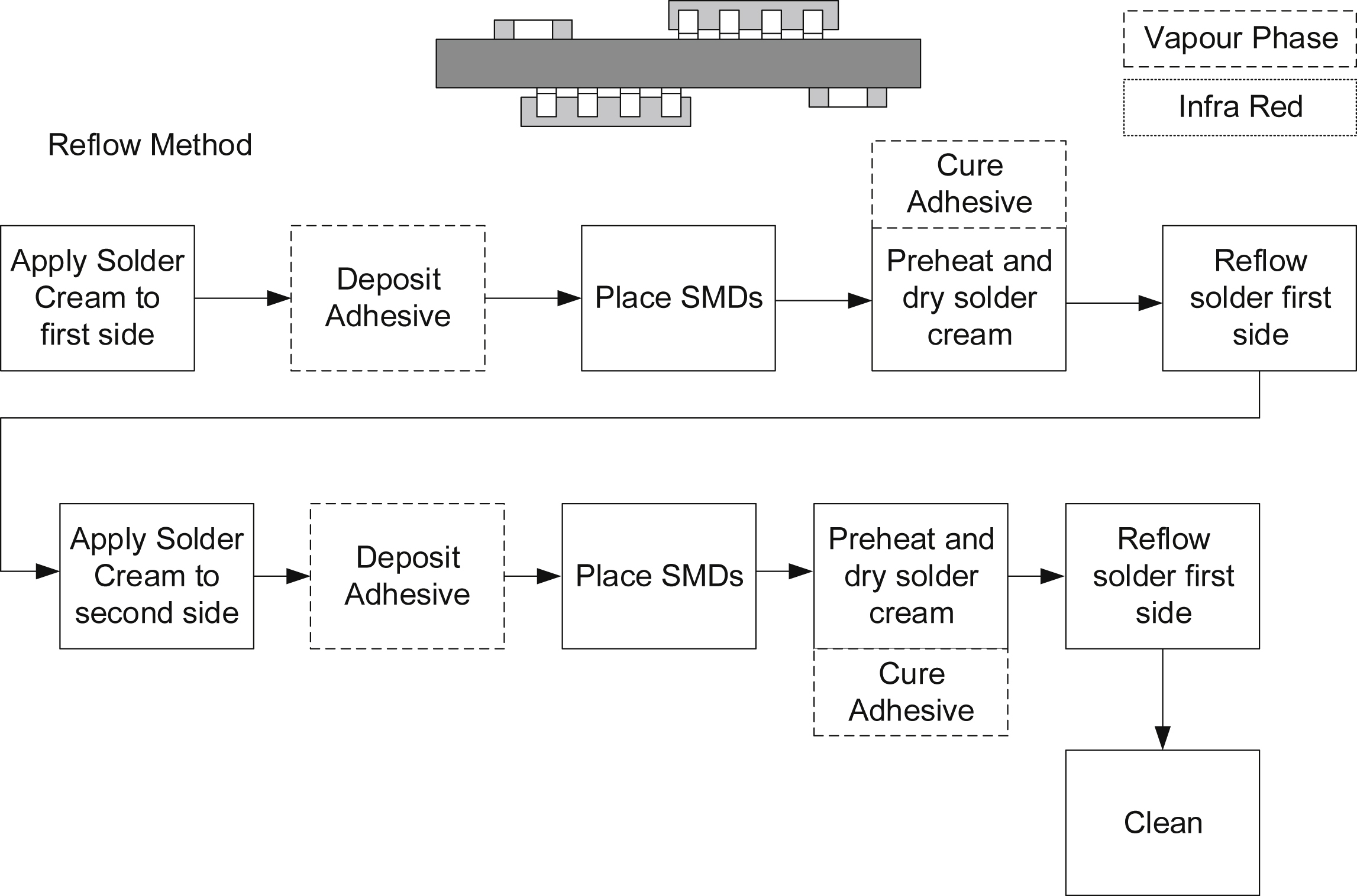

Vapor phase or infrared soldering allows tighter packing and smaller pads, and the orientation is not critical. When the solder paste reflows, surface tension will draw misaligned components into line with their pads, so that placement tolerance is less critical. Shadowing can be a problem with components of varying height placed close together, as can variable heat absorption if there are large and small packages with different heat reflection coefficients. Board layout must start from the knowledge of which soldering method will be used and also what tolerances will be encountered in the placement process and in the components themselves. If wave soldering pad dimensions are used for reflow soldering, solder joint quality will suffer. Most layout designers use different pad dimensions for the two systems.
Printed Circuit Board Quality
pcb finish is more important than it is with through hole components. The overriding requirement is flatness of the surface, since component sizes are that much smaller and since good soldered joints depend on close contact of the leadouts with the pads. A solder resist is essential to control the soldering process. Photo-imageable film resists are to be preferred to screen printed (see Section 2.2.6) since their thickness is well controlled also because the tolerances on solder mask windows are that much tighter. There must be no bleeding of the resist onto the pads. Hot air leveling of the tin/lead finish on the solder pads is usual to prevent the bumps that form on the surface of ordinary reflowed tin/lead.
Thermal Stresses
Differential thermal expansion is a potential reliability threat for some SM components. Chip resistors and capacitors, and leadless chip carriers (LCCs), are made with a ceramic base material whose coefficient of thermal expansion is not well matched to epoxy fiberglass. Originally these components were developed for hybrid circuits, which use ceramic substrates, and for which good thermal matching is possible. At the same time, leadouts for these components are deposited directly on the ceramic so that there is no compliance between the leadout (at the soldered joint) and the case. As a result, strains set up under thermal cycling can crack the component itself or the track to which it is soldered.
You should not therefore use the larger ceramic or LCC components directly on epoxy fiberglass board. Leaded SM components such as small outline or flat-pack ICs do not suffer from this problem because there is a section of compliant lead between the soldered joint and the package. Plastic-leaded chip carriers with J-lead construction are useable for the same reason, and small chip ceramic components are also useable because of their small size.
Cleaning and Testing
Cleaning an SM board is trickier than for a through hole assembly because there is less of a gap underneath the packages. Flux contamination can get into the gaps but it is harder to flush out with conventional cleaning processes. There is considerable effort being put into developing solder fluxes that do not need to be cleaned off afterward.
Testability is an important consideration. It is bad practice to position test probes directly over component leadouts. Apart from the risk of component damage, the pressure of the probe could cause a faulty joint to appear sound. All test nodes should be brought out to separate test pads, which have no component connections to them, and which should be on the opposite side of the board to the components. There is an extra board space overhead for these pads, but they need be no more than 1 mm in diameter. Testing a double-sided densely packed SM assembly is a nightmare (see Section 9.3.3).
2.3.2. Package Placement
There is a mix of electrical and mechanical factors to consider when placing components and ICs. Normally the foremost is to ensure short, direct tracks between components, and it is always worth interactively optimizing the placement and track routing to achieve this. You may also face thermal constraints, for instance, precision components should not be next to ones that dissipate power, or you may have to worry about heat removal.
Over and above individual requirements there is also the general requirement of producibility. There should be continuous feedback between you as circuit designer and the production and service departments to make sure that products are easy, and therefore cheap, to produce and repair. Component and package placement rules should evolve with the capabilities of the production department. Some examples of producibility requirements follow:
• pick-and-place and auto insertion machines work best when components and packages are all facing the same way and are positioned on a well-defined grid
• small tubular components (resistors, capacitors, and diodes) should conform to a single lead pitch to minimize the required tooling heads. It does not matter what it is (0.4″ and 0.5″ are popular) as long as it's constant
• inspection is easier if all ICs are placed in the same orientation, i.e., with each pin one facing the same corner of the board, and similarly all polarized components are facing the same way
• spacing between components should take into account the need to get test probes and auto insertion guides around each component
• spacing of components from the board edges depends on handling and wave soldering machinery, which may require a clear area (sometimes called the “stacking edge”) on one or two edges
• if the board is to be wave soldered, rows of adjacent pins are best oriented across the direction of flow, parallel to the wave, to reduce the risk of solder bridges between pins or pads.
2.3.3. Component Identification
Most pcbs will have a legend, usually yellow or white, screen printed on the component side to describe the position of the components. This can be useful if assembly of the finished unit relies on manual insertion, but its major purpose is for the test and service departments to assist them in seeing how the board relates to its circuit diagram. With low-to-medium density boards you can normally find space beside each component to indicate its number, but as boards become more densely packed this becomes increasingly difficult. Printing a component's ID underneath it is of no use to the service engineer, and if component placement is automatic, it's no use to the production department either. Particularly if the board consists almost entirely of small outline or DIL ICs, these can be identified by a grid reference system with the grid coordinates included on the component side track artwork. Therefore you should consider whether the extra expense of printing the legend onto a high-density board is justified.
Assuming it is, there are a few points to bear in mind when creating the legend master. If possible, print onto flat surfaces, not over edges of tracks or pads; the uneven surface tends to blur the print quality. Never print ink over or near a hole (allowing for tolerances). Even if it's not a solderable hole, the unprinted ink will build up on the screen and after several passes will leave a blot, ruining the readability. If there are large numbers of vias, these should be filled in or “tented” to prevent the holes remaining and rendering areas of the board useless for legend printing.
Polarity Indication
There are several ways of indicating component polarity on the legend. Really the only criterion for these should be legibility with the component in place, so that they are as useful to inspectors and test engineers as they are to the assembly operators. Once a particular method has gained acceptance, it should be adhered to; using different polarity indicators on different boards (or even on the same board) is a sure way of confusing production staff and gaining faulty boards.
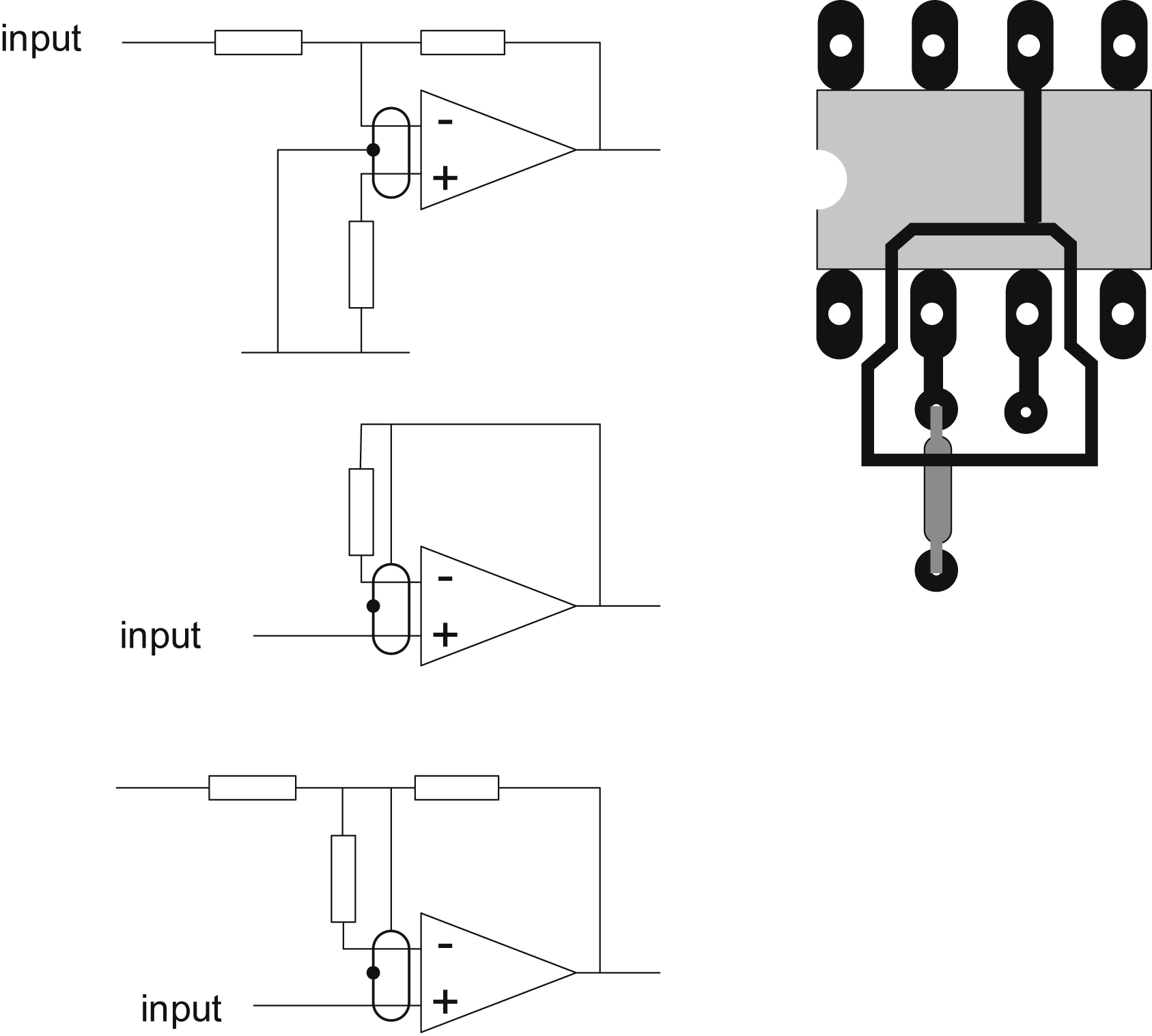
Guarding
The next level of defense is guarding. This technique accepts that there will be some degree of leakage to the high impedance node, but minimizes the current flow to it by surrounding it with a conductive trace that is connected to a low impedance point at the same potential. Like the similar circuit technique of bootstrapping, if the voltage difference between two nodes is forced to be very low, the apparent resistance between them is magnified. The electrical connections and pc layouts for the guards for the basic op-amp input configurations are shown in Fig. 2.32. The guard effectively absorbs the leakage from other tracks, reducing that reaching the high impedance point.
There should be a guard on both sides of a double-sided board. Although the guard virtually eliminates surface leakage, it has less effect on bulk leakage through the board; fortunately this is orders of magnitude higher than leakage due to surface contamination. The width of the guard track is unimportant as far as surface resistance goes, but a wider guard will improve the effect on bulk resistance.
Guarding is a very useful technique but obviously requires some extra thought in circuit design. Generally, you should consider it in the early design stages whenever you are working with impedance levels, which are susceptible to surface resistance variations. You may then be in the happy position of never noticing the problem.
2.3.4. Understanding Thermal Behavior
There are three main methods by which heat may be transmitted through a medium (such as air or pcb material):
• Convection
• Conduction
• Radiation
Of these, convection and conduction are of the most interest from a design point of view, as they can be a controllable method of removing heat from the components in the system; however, radiation, however, is less controllable and is potentially a problem. The heat generated by a component(s) or intrinsic to an environment can readily radiate to other components causing potential problems.
Thermal Conduction
Conduction is the mechanism for transfer of energy between materials at different temperatures.
The heat flow rate Q through a material (Fig. 2.33) can be calculated across a material of infinitesimally small thickness dx, with a temperature difference across it of dT using the expression:
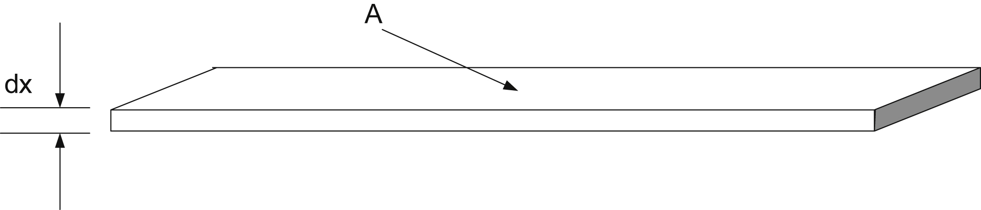
If the steady-state condition has been reached, such that the temperature on one side of the block is TH and TL on the other, Q can be expressed simply as in Eq. (2.2):
where k is the thermal conductivity, and L is the length of the material.
The thermal resistance can be defined using Eq. (2.3):
Thermal Convection
In contrast to conduction where the heat flow is through a static solid material, convection cooling occurs through a gas or fluid medium. The most common form of convection cooling is air cooling via a heat sink. In convection cooling systems, it is the movement of the medium (air or fluid) that carried the heat from the hot areas in the system to the cold.
The reason why heat sinks have fins is to present as large a surface area as possible to the medium to transport the heat away from the device. The thermal resistance can be drastically reduced in a convection cooling approach by using a forced air cooling system. If the system does not have forced air, it is called natural convection cooling; however, if the system has forced air it is called forced convection cooling.
The improvement that forced convection can bring is significant. At sea level the following expression can be used to estimate the air flow (in cfm—cubic feet per minute or lpm—liters per minute) required to dissipate a power loss at a specific temperature difference
Thermal Radiation
Radiation cooling is a problem in power supplies as it is difficult to establish a clear path for extraction of excess heat using this method. Instead, the heat radiates in all directions and may cause problems with components nearby. The radiated power loss is proportional to the difference of temperatures to the power of 4 (Stefan–Boltzmann Law) in Eq. (2.6):
where E is the emissivity of the material, with some example values of surface emissivity given in Table 2.3.
Thermal Capacity
The thermal capacity (or specific heat) is a term that causes apparent discrepancies with the thermal behavior of materials, and the thermal capacity is analogous to a capacitor in the electrical domain and influences how fast a material heats up. As an example, if a heat exchanger has a high thermal capacity, it will take some time for the final temperature to be reached, but it will be the same final temperature as a heat exchanger with the same thermal resistance but lower thermal capacity (Fig. 2.34).


Thermal Expansion
Thermal Shock
Materials expand and contract naturally depending on the thermal conditions prevalent. Thermal shock is defined as the failure or fracture of a materials or structure due to stresses induced by thermal expansion. One aspect of this is manifest if two materials with different expansion coefficients are bonded together and the electronics cause a significant heat rise.
In this instance, the materials may be cracked if the rates of expansion are different enough for the resulting stresses to cause a structural failure. The stress in a material can be estimated by calculating the expansion and then applying Hooke's Law (F = −kx) to obtain the stress.
Thermal Cycling
As the changes in temperature will cause mechanical stress in materials, it is useful to consider various types of temperature cycling. There may be significant stresses in the die and substrate of power devices due to localized temperature variations.
There are also variations in environmental temperatures as the weather changes or in the operating environment (PC, Car Engine, Aircraft, Spacecraft). Thermal stress will occur also as the materials cool down, so the stresses are applied to the materials as they continuously expand and contract. The thermal cycling may also have a significant effect on other mechanically related aspects of the system such as solder joints.
Solder Cracking
Solder cracking can occur internally or externally.
• Internal solder cracks occur where the solder itself is cracked. This is especially insidious as it may be very difficult to spot or pinpoint the fault until a failure occurs.
• External solder cracks occur between the solder and the surface to which the solder is bonded.
The Impact of Thermal Stress on Reliability
The reliability of components will be adversely affected by any form of electrical and/or thermal stress. A typical approach to calculating the mean time before failure, usually specified in hours, is to take the base failure rate and add electrical and thermal stress “accelerators” to estimate the true reliability under fault conditions:
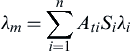 (2.7)
(2.7)where Ati = thermal accelerator; Si = electrical accelerator; λi = base failure rate; n = number of modules.
The key term in this context is the thermal accelerator (A), which can be estimated using Eq. (2.8):
 (2.8)
(2.8)where k = Boltzmann's constant (8.6e-5); ea = eV; Tref = reference temperature (K); Top = operational temperature (K)
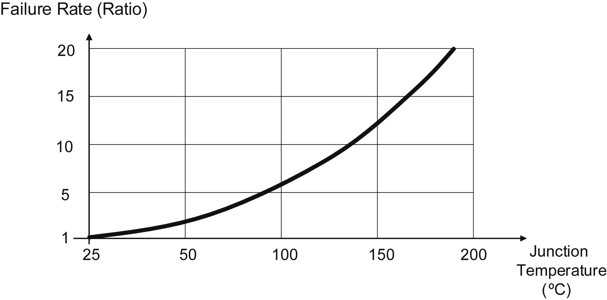
The change in failure rate can be seen graphically as the temperature increases in Fig. 2.37. In this case the failure rate is a ratio with respect to the base failure rate at 25°C.
2.4. Surface Protection
The insulation resistance between adjacent conductors on a bare pcb surface depends on the conductor configuration, the surface resistance of the base material, processing of the board, and environmental conditions, particularly temperature, humidity, and contamination. For a new board with no surface contamination the expected insulation resistance between two parallel conductors can be derived from:
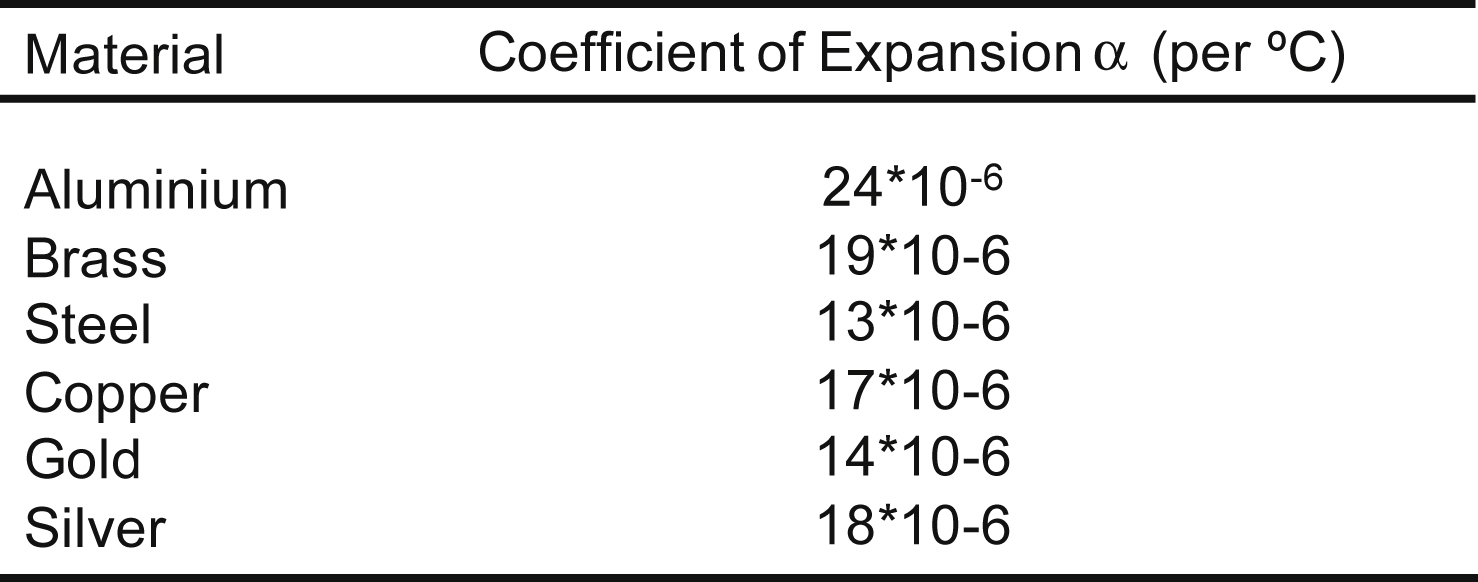
where Rm is the material's surface resistance specification at a given temperature; (see Table 2.1); w is the track spacing; l is the length of the parallel conductors.
Variations in Surface Resistance
Generally this value is of the order of thousands of megohms and could be safely ignored for most circuits. Unfortunately it is not likely to be the actual value you would measure. This is because plating and soldering processes, dust and other surface contamination, moisture absorption, and temperature variation will all have the effect of lowering the insulation resistance. Variations between 10 and 1000 times less can be observed under normal operating conditions, and a severe environment can reduce it much more.
When you are working with high impedance or precision circuits you may not be able to ignore the change in surface resistance. Until you realize what the problem is, its effects can be mysterious and hard to pin down: they include variability of circuit parameters with time of day, handling of the board, weather (relative humidity), location and orientation of the assembly, and other such factors that normally you would expect to be irrelevant. Typical variations are change of bias point on high input impedance amplifiers and unreliable timing on long time constant integrators.
Circuit Design Versus Surface Resistance
There are a number of strategies you can use to combat the effects of surface resistance. The first and most obvious is to keep all circuit operating impedances as low as possible, so that the influence of an unstable parallel resistance in the megohm region is minimal. In some cases—micropower circuits and transducer inputs, for example—you do not have the option. In other cases a change in circuit philosophy could be beneficial; a long time constant analogue integrator or sample and hold might be replaced by its digital equivalent, with an improvement in accuracy and repeatability.
If there is a particular circuit node, which must be maintained at a high impedance, the wiring to this can be kept off the board by taking it to a PTFE stand-off insulator. PTFE has excellent surface resistance properties even in the presence of contamination. Alternatively, reducing the length of high impedance PC tracks and increasing their distance from other tracks may offer enough improvement, at the expense of packing density. Simply rerouting an offending track might help: if a power rail is run past a high impedance node, which is biased near 0 V, you have an unwanted potential divider that will pull the bias voltage up by an unpredictable amount. Put the power rail track elsewhere.
2.4.1. Conformal Coating
If none of the above methods are sufficient, or if they are inapplicable, or if the working environment of the board is severe (relative humidity approaching 100%, conductive or organic contamination present, corrosive atmosphere), then you will have to go for conformal coating. This is not a decision to be taken lightly; try everything else first. Coating adds pain, sweat, and expense to the production process; and the following discussion will outline why.
Coating Versus Encapsulation
Note that conformal coating is not the same as encapsulation, or potting, which is even less desirable from a production point of view. Encapsulation fills the entire unit with solid compound so that the end result looks rather like a brick and is used to prevent third parties from discovering how the circuit works, or to meet safety approvals, or for environmental or mechanical protection. A badly potted unit will probably work like a brick too: differential thermal expansion as the resin cures can crack poorly anchored pc tracks, and the faulty result is unrepairable. Conformal coating covers the board with thin coats of a clear resin so that the board outlines and components are still visible. It provides environmental protection only. Occasionally it may help in meeting safety approval clearances but this is rare.
The main environmental hazard against which conformal coating protects is humidity. The popular coating types, acrylics, polyurethanes, epoxy resins, and silicones are all moistureproof. Most offer protection against the common chemical contaminants: fluxes, release agents, solvents, metal particles, finger grease, food and cosmetics, salt spray, dust, fuels, and acids. Acrylics are rather less resistant to chemical attack than the others. A conformal coating will not allow closer track spacing when this is determined by the surface insulation properties of the board, but it does eliminate degradation of these properties by environmental factors: if it is used properly.
Steps to Take Before Coating
The first point to remember is that a conformal coating seals in as well as out. The cleanliness of the board and its low moisture content are paramount. If residual contaminants are left under the film, corrosion and degradation will continue and will eventually render the coating useless. A minimum of three steps must be followed immediately prior to coating:
• vapor degrease in a solvent bath (note that with increasing concern about environmental pollution and ozone depletion, traditional cleaning fluids, particularly CFCs, are being phased out)
• rinse in deionized water or ethyl/isopropyl alcohol to dissolve inorganic salts
• oven bake for 2 h at 65–70°C (higher if the components will allow it) to remove any residual solvent and moisture.
After cleaning and baking, the assembly should only be handled with rubber or lint free gloves. If the cleaned boards are left for any appreciable time before coating, they will start to reabsorb atmospheric moisture, so they should be packed in sealed bags with .
Application
The coating can be applied by dipping or spraying. The application process must be carefully controlled to produce a uniform, complete coat. Viscosity and rate of application are both critical. At least two and preferably three coats should be applied, air- or oven-drying between each, to guard against pinholes in each coat. Pot life of the coating material—the length of time it is useable before curing sets in—is a critical parameter since it determines the economics of the application process. Single-component solvent-based systems are preferable to two-part resins in this respect and also because they do not need metering and mixing, a frequent source of operator error. On the other hand, solvent-based systems require greater precautions against operator health hazards and flammability.
Nearly all boards will require breaks in the coating, for connectors or for access to trimming components and controls. Aside from the question of the environmental vulnerability of these unprotected areas, such openings require masking before the board is coated, and removal of the mask afterward. Manual application of masking tape and semiautomatic application of thixotropic latex-based masking compound are two ways to achieve this.
Test and Rework
Finally, once the board is coated, there is the difficult problem of test, rework, and repair. By its nature the coating denies access to test probes, so all production testing must be done before the coating stage. Acrylics and polyurethanes can be soldered through or dissolved away to achieve a limited degree of rework but other types cannot. After rework, the damaged area must be cleaned, dried, and recoated to achieve a proper seal. Ease of rework and ease of application are often the most important considerations in choosing a particular type of coating material.
You might now appreciate why conformal coating is never welcome in the production department. Because it is labor-intensive, it can easily double the overall production cost of a given assembly. Specify it only after long and careful consideration of the alternatives.
2.5. Sourcing Boards and Artwork
Before we leave the subject of pcbs, a short discussion of board procurement is in order. There are two stages involved: generation of the artwork and associated documents and production of the boards. The two are traditionally separated because different firms specialize in each, so that having generated the artwork from one source you would take it to another to have the boards made. Some larger pcb firms have both stages in-house or have associated operations for each.
2.5.1. Artwork
The artwork includes the track and solder resist patterns, the hole drilling diagram, the component legend, and a dimensional drawing for the board. The patterns are generated photographically, generally direct from CAD output. To create the artwork you can either do it yourself in-house using your CAD system or you can take the work to a bureau that specializes in PC artwork and has its own CAD system. There are advantages and trade-offs both ways.
Using a Bureau
So you may be faced with the choice of going to an outside bureau. Reasons for doing this are if
• your own company does not have any artwork facilities at all;
• you do have the facilities but they are insufficient for or inappropriate to your design;
• you have all the facilities you need but they are not available in the timescale required.
There are less tangible advantages of a bureau. Its staff must by nature all be highly skilled and practiced layout draftsman, and they should be using reasonably up-to-date and reliable CAD systems, so the probability of getting a well-designed board out in a short time may be higher than if you did it in-house. They will also be able to give you guidance in the more esoteric aspects of pcb design that you may not be familiar with. This can be particularly important for new surface mount designs, or those with severe performance requirements such as high-speed critical track routes. A bureau that is interested in keeping its customers will be flexible with its timescales. Even the cost should be no more than you would have to pay in-house, since the bureau is using its resources more efficiently. Finally, a bureau that works closely with a board manufacturer will be able to generate artwork that is well matched to his requirements, thereby freeing you of an extra and possibly unfamiliar specification burden.
Disadvantages of a Bureau
There are three possible disadvantages. One is confidentiality: if your designs go outside, there is always the possibility that they will be compromised, whatever assurances the bureau may give. Another is that you are then locked in to that bureau for future design changes, unless you happen to have the same CAD system (remembering that even different software versions of the same system can be incompatible) in-house. The risk is that the bureau might not be as responsive to requests for changes in the future as it would be to the first job. You have to balance this against what you know of the bureau's past history.
Finally, you may feel that you have less control over the eventual layout. This is not such a threat as it may seem. You always have the option to go and look over the layout designer's shoulder while they are doing the work; select a bureau nearby to avoid too much travel. Or, use e-mail to review the design as it continues, at defined stages in the process. Even if you do not have the same CAD system in-house, the artwork can be viewed in standard Gerber format using the freely available GCPrevue software.
But more importantly, giving your design to an outsider imposes the very beneficial discipline that you need to specify your requirements carefully and in detail. Thus you are forced to do more rigorous design work in the early stages, which in the long run can only help the project.
2.5.2. Boards
PCB suppliers are not thin on the ground. It should be possible to select one who can offer an acceptable mix of quality, turnround, and price. There is, though, a lot of work involved in doing this, and once you have established a working relationship with a particular supplier it is best to stay with him, unless he or she lets you down badly. Any board manufacturer should be happy to show you round his or her facilities and should be able to be specific about the manufacturing limits to which he or she can work. You may also derive some assurance from going to a quality-assessed supplier, or it may be company policy to do so. While market competition prevails, using a quality-assessed supplier should be no more expensive than not.
The major difference lies between sourcing prototype and production quantity boards. In the prototype stage, you will want a small quantity of boards, usually no more than half a dozen, and you will want them fast. A couple of weeks later you will have found the errors and you will want another half a dozen even faster because the deadline is looming. The fastest turnround offered on normal double-sided PTH boards is four or 5 days, and the cost for such a “prototype service” is between two and five times that for production quantities with several weeks' lead time.
Sometimes you can find a manufacturer who can offer both reasonable production and prototype services. Usually though, those who specialize in prototype service do not offer a good price on production runs, and vice versa. If you manage to extract a fast prototype service on the promise of production orders, you then have to explain to the purchasing department why they cannot shop around for the lowest price later. This can be embarrassing; on the other hand they may be operating under other constraints, such as incoming quality. There are several trade-offs that the purchasing department has to make, which may not be obvious to you, and it pays to involve them throughout the design process.
The board supplier will want a package of information, which is more than just the board artwork. A typical list would include the following:
• Artwork for all copper layers
• Artwork for solder mask layers
• Ident layers, peelable layers, carbon layers—where applicable
• Drilling data
• Drawings for a single pcb or pcb panel if applicable
• Details of material specifications to be used—usually you will refer to the board manufacturer's own standard materials
• Metallic finish required
• Solder mask and ident—type and color
• Layer build details
• Testing requirements
It would be typical to have a “boilerplate” specification, which applies to all boards used in-house and which covers all these points in a standard way, so that only the differences need to be considered in depth for a particular board design.
..................Content has been hidden....................
You can't read the all page of ebook, please click here login for view all page.