Chapter 9
General Product Design
Abstract
Any electronic equipment must be designed for safe operation. Most countries have some form of product liability legislation that puts the onus on the manufacturer to ensure that his product is safe. The responsibility devolves onto the product design engineer, to take reasonable care over the safety of the design. This includes ensuring that the equipment is safe when used properly, that adequate information is provided to enable its safe use, and that adequate research has been carried out to discover, eliminate, or minimize risks due to the equipment.
Keywords
Bed-of-nails probing; Boundary-scan testing; Derating; Mean time between failure; Reliability; Thermal equivalent circuits
9.1. Safety
Any electronic equipment must be designed for safe operation. Most countries have some form of product liability legislation that puts the onus on the manufacturer to ensure that his product is safe. The responsibility devolves onto the product design engineer, to take reasonable care over the safety of the design. This includes ensuring that the equipment is safe when used properly, that adequate information is provided to enable its safe use, and that adequate research has been carried out to discover, eliminate, or minimize risks due to the equipment.
There are various standards relating to safety requirements for different product sectors. In some cases, compliance with these standards is mandatory. In the European Community, the Low Voltage Directive (73/23/EEC) applies to all electrical equipment with a voltage rating between 50- and 1000-V ac or 75 and 1500-V dc, with a few exceptions and requires member states to take all appropriate measures
to ensure that electrical equipment may be placed on the market only if, having been constructed in accordance with good engineering practice in safety matters in force in the Community, it does not endanger the safety of persons, domestic animals or property when properly installed and maintained and used in applications for which it was made.
If the equipment conforms to a harmonized CENELEC or internationally agreed standard then it is deemed to comply with the Directive. Examples of harmonized standards are EN 60065:1994, “Safety requirements for mains-operated electronic and related apparatus for household and similar general use,” which is largely equivalent to IEC Publication 60065 of the same title; or EN 60950-1:2002, “Information technology equipment. Safety. General requirements,” equivalent to IEC 60950-1. Proof of compliance can be by a Mark or Certificate of Compliance from a recognized laboratory, or by the manufacturer's own declaration of conformity. The Directive includes no requirement for compulsory approval for electrical safety.
9.2. The Hazards of Electricity
The chief dangers (but by no means the only ones, see Table 9.1) of electrical equipment are the risk of electric shock and the risk of a fire hazard. The threat to life from electric shock depends on the current that can flow in the body. For ac, currents less than 0.5 mA are harmless, while those greater than 50–500 mA (depending on duration) can be fatal.1 Protection against shock can be achieved simply by limiting the current to a safe level, irrespective of the voltage. There is an old saying, “it's the volts that jolts, but the mils that kills.” If the current is not limited, then the voltage level in conjunction with contact and body resistance determines the hazard. A voltage of less than 50-V ac rms, isolated from the supply mains or derived from an independent supply, is classified as a safety extra-low voltage (SELV) and equipment designed to operate from an SELV can have relaxed requirements against the user being able to contact live parts.
Aside from current and voltage limiting, other measures to protect against electric shock are as follows:
• Earthing and automatic supply disconnection in the event of a fault. See Section 1.1.12.
• Inaccessibility of live parts. A live part is any part, contact with which may cause electric shock, that is any conductor, which may be energized in normal use—not just the mains “live.”
Table 9.1
Some Safety Hazards Associated With Electronic Equipment
| Hazard | Main Risk | Source |
| Electric shock | Electrocution, injury due to muscular contraction, burns | Accessible live parts |
| Heat or flammable gases | Fire, burns | Hot components, heat sinks, damaged or overloaded components and wiring |
| Toxic gases or fumes | Poisoning | Damaged or overloaded components and wiring |
| Moving parts, mechanical instability | Physical injury | Motors, parts with inadequate mechanical strength, heavy or sharp parts |
| Implosion/explosion | Physical injury due to flying glass or fragments | CRTs, vacuum tubes, overloaded capacitors, and batteries |
| Ionizing radiation | Radiation exposure | High-voltage CRTs, radioactive sources |
| Nonionizing radiation | RF burns, possible chronic effects | Power RF circuits, transmitters, antennas |
| Laser radiation | Damage to eyesight, burns | Lasers |
| Acoustic radiation | Hearing damage | Loudspeakers, ultrasonic transducers |
9.2.1. Safety Classes
IEC publication 60536 classifies electrical equipment into four classes according to the method of connection to the electrical supply and gives guidance on forms of construction to use for each class. The classes are
Class 0: Protection relies on basic functional insulation only, without provision for an earth connection. This construction is unacceptable in the United Kingdom.
Class I: Equipment is designed to be earthed. Protection is afforded by basic insulation, but failure of this insulation is guarded against by bonding all accessible conductive parts to the protective earth conductor. It depends for its safety on a satisfactory earth conductive path being maintained for the life of the equipment.
Class II: The equipment has no provision for protective earthing, and protection is instead provided by additional insulation measures, such as double or reinforced insulation. Double insulation is functional insulation, plus a supplementary layer of insulation to provide protection if the functional insulation fails. Reinforced insulation is a single layer, which provides equivalent protection to double.
Class III: Protection relies on supply at SELV and voltages higher than SELV are not generated. Second-line defenses such as earthing or double insulation are not required.
9.2.2. Insulation Types
As outlined above, the safety class structure places certain requirements on the insulation that protects against access to live parts. The basis of safety standards is that there should be at least two levels of protection between the casual user and the electrical hazard. The standards give details of the required strength for the different types of insulation, but the principles are straightforward.
Basic Insulation
Basic insulation provides one level of protection but is not considered fail-safe, and the other level is provided by safety earthing. A failure of the insulation is therefore protected against by the earthing system.
Double Insulation
Earthing is not required because the two levels of protection are provided by redundant insulation barriers, one layer of basic plus another supplementary; if one fails the other is still present, and so this system is regarded as fail-safe. The double-square symbol indicates the use of double insulation.
Reinforced Insulation
Two layers of insulation can be replaced by a single layer of greater strength to give an equivalent level of protection.
9.2.3. Design Considerations for Safety Protection
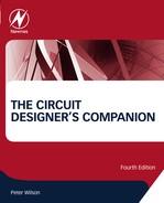
The requirement for inaccessibility has a number of implications. Any openings in the equipment case must be small enough that the standard test finger, whose dimensions are defined in those standards that call up its use, cannot contact a live part (Fig. 9.1). Worse, small suspended bodies (such as a necklace) that can be dropped through ventilation holes must not become live. This may force the use of internal baffles behind ventilation openings.
Protective covers, if they can be removed by hand, must not expose live parts. If they do, they must only be removable by use of a tool. Or, use extra internal covers over live portions of the circuit. It is anyway good practice to segregate high-voltage and mains sections from the rest of the circuit and provide them with separate covers. Most electronic equipment runs off voltages below 50 V and, provided the insulation offered by the mains isolating transformer is adequate, the signal circuitry can be regarded as being at SELV and therefore not live.
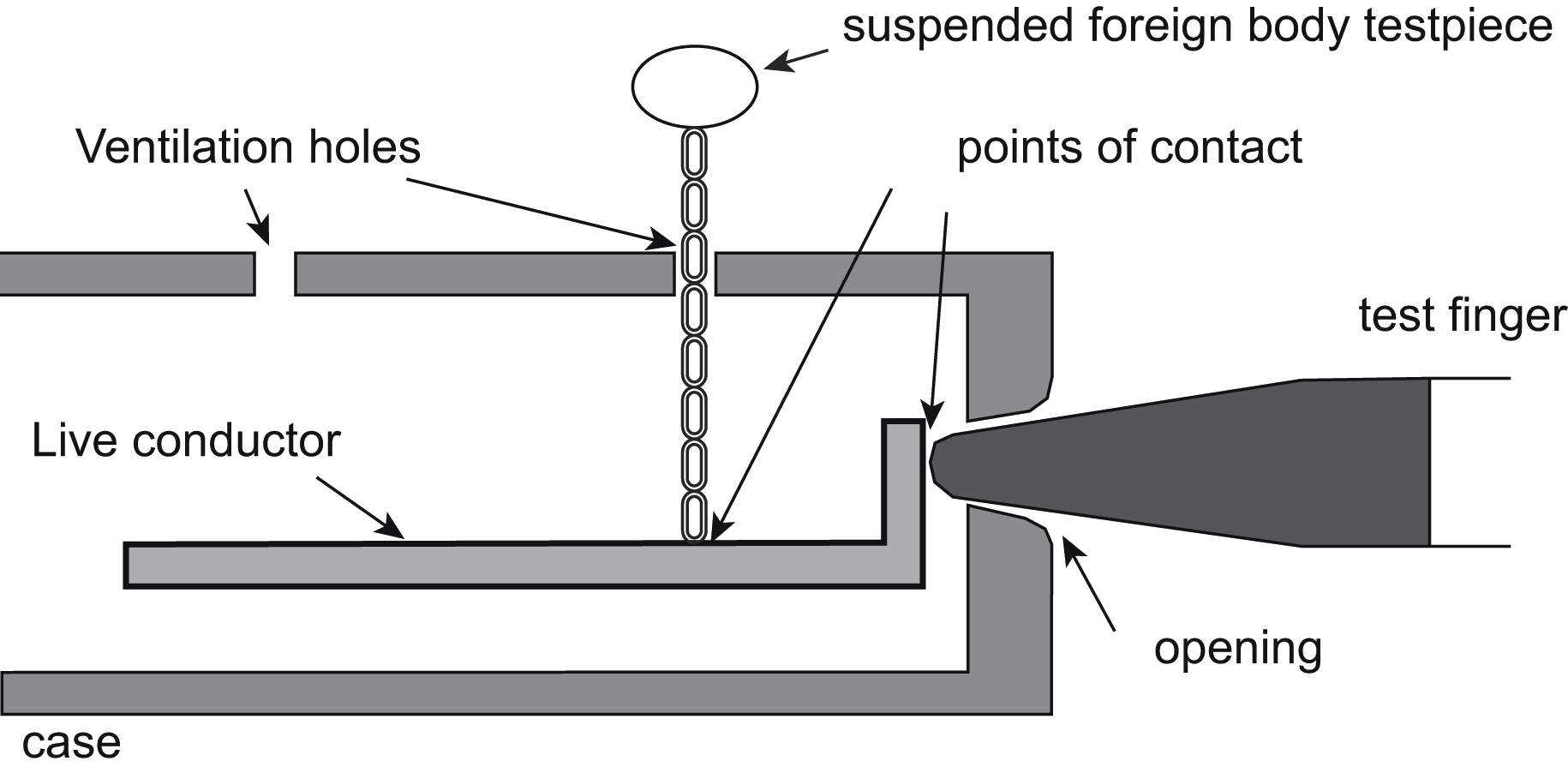
Any insulation must, in addition to providing the required insulation resistance and dielectric strength, be mechanically adequate. It will be dropped, impacted, scratched, and perhaps vibrated to prove this. It must also be adequate under humid conditions: hygroscopic materials (those that absorb water readily, such as wood or paper) are out. Various standards define acceptable creepage and clearance distances versus the voltage proof required. As an example, EN 60065 allows 0.5 mm below 34 V rising to 3 mm at 354 V and extrapolated thereafter; distances between PCB conductors are slightly relaxed, being 0.5 mm up to 124 V, increasing to 3 mm at 1240 V. Creepage distance (Fig. 9.2) denotes the shortest distance between two conducting parts along the surface of an insulating material, while clearance distance denotes the shortest distance through air.
Easily discernible, legible, and indelible marking is required to identify the apparatus and its mains supply, and any protective earth or live terminals. Mains cables and terminations must be marked with a label to identify earth, neutral, and live conductors, and class I apparatus must have a label which states “WARNING: THIS APPARATUS MUST BE EARTHED”. Fuse holders should also be marked with their ratings and mains switches should have their “off” position clearly shown. If user instructions are necessary for the safe operation of the equipment, they should preferably be marked permanently on the equipment.
Any connectors that incorporate live conductors must be arranged so that exposed pins are on the dead side of the connection when the connector is separated. When a connector includes a protective earth circuit, this should mate before the live terminals and unmate after them. (See the CEE-22 6A connector for an example.)
9.2.4. Fire Hazard
It is taken for granted that the equipment will not overheat during normal operation. But you must also take steps to ensure that it does not overheat or release flammable gases to the extent of creating a fire hazard under fault conditions. Any heat developed in the equipment must not impair its safety. Fault conditions are normally taken to mean short circuits across any component, set of terminals or insulation that could conceivably occur in practice (creepage and clearance distances are applied to define whether a short circuit would occur across insulation), stalled motors, failure of forced cooling, and so on.
The normal response of the equipment to these types of faults is a rise in operating current, leading to local heating in conductors. The normal protection method is by means of current limiting, fuses, thermal cutouts, or circuit breakers in the supply or at any other point in the circuit where overcurrent could be hazardous. As well as this, flame-retardant materials should be used wherever a threat of overheating exists, such as for PCB base laminates.
Fuses are cheap and simple but need careful selection in cases where the prospective fault current is not that much higher than the operating current. They must be easily replaceable, but this makes them subject to abuse from unqualified users (hands up anyone who has not heard of people replacing fuse links with bent nails or pieces of cigarette-packet foil). The manufacturer must protect his liability in these cases by clear labeling of fuse holders and instructions for fuse replacement. Fuse specification is covered in more detail in Section 7.2.3.
Thermal cutouts and circuit breakers are more expensive but offer the advantage of easy resetting once the fault has cleared. Thermal devices must obviously be mounted in close thermal contact with the component they are protecting, such as a motor or transformer.
9.3. Design for Production
Really, every chapter in this book has been about design for production. As was implied in the introduction, the ability that marks out a professional designer is the ability to design products or systems, which work under all relevant circumstances and which can be manufactured easily.
The sales and marketing engineer addresses the questions, “can I sell this product?” and “how much can I sell this product for?” This book has not touched on these issues, important though they are to designers; it has assumed that you have a good relationship with your marketing department and that your marketing colleagues are good at their job. But you as designer also have to address another set of questions, which includes the following:
• Can the purchasing department source the components quickly and cheaply?
• Can the production department make the product quickly and cheaply?
• Can the test department test it easily?
• Can the installation engineers or the customer install it successfully?
It is as well to bear all these questions in mind when you are designing a product, or even part of one. Your company's financial health, and consequently your and others' job security, ultimately depends on it. A good way to monitor these factors is to follow a checklist.
9.3.1. Checklist
Sourcing
• Have you involved purchasing staff as the design progressed?
• Are the parts available from several vendors or manufacturers wherever possible? Have you made extensive use of industry standard devices?
• Where you have specified alternate sources, have you made sure that they are all compatible with the design?
• Have you made use of components that are already in use on other products?
• Have you specified close-tolerance components only where absolutely necessary?
• Where sole-sourced parts have to be used, do you have assurances from the vendor on price and lead time? How reliable are they? Have you checked that there is no warning, “not recommended for new designs” (implying limited availability), on each part?
• Does your company have a policy of vetting vendors for quality control? If so, have you added new vendors with this product, and will they need to be vetted?
Production
• Have you involved production staff as the design progressed?
• Are you sure that the mechanical and electrical design will work with all mechanical and electrical tolerances?
• Does the mechanical design allow the component parts to be fitted together easily?
• Are components, especially polarized ones, all oriented in the same direction on the PCB for ease of inspection and insertion?
• Are discrete components, notably resistors, capacitors, and transistors, specified to use identical pitch spacings and footprints as far as possible?
• Have you minimized wiring looms to front or rear panels and between PCBs, and used mass-termination connections (e.g., insulation displacement connector) wherever possible?
• Have you modularized the design as far as possible to make maximum use of multiple identical units?
• Is the soldering and assembly process (wave, infrared, autoinsert, pick and place, etc.) that you have specified compatible with the manufacturing capability? Will the placement machines cope with all the surface-mount components you have used?
• If the production calls for any special assembly procedures (e.g., potting or conformal coating), or if any components require special handling or assembly (MOSFETs, LEDs, batteries, relays, etc.) are the production and stores staff fully conversant with these procedures and able to implement them? Have you minimized the need for such special procedures?
• Do all PCBs have adequate solder mask, track and hole dimensions, clearances, and silk screen legend for the soldering and assembly process? Are you sure that the test and assembly personnel are conversant with the legend symbols?
• Are your assembly drawings clear and easy to follow?
Testing and Calibration
• Have you involved test staff as the design progressed?
• Are all adjustment and test points clearly marked and easily accessible?
• Have you used easily set parts such as dual in line switches or linking connectors in preference to solder-in wire links?
• Does the circuit design allow for the selection of test signals, test subdivision, and stimulus/response testing (including boundary scan) where necessary?
• If you are specifying automatic testing with automatic test equipment (ATE), does the pc layout allow adequate access and tooling holes for bed-of-nails probing? Have you confirmed the validity of the ATE program and the functional test fixture?
• Have you written and validated a test software suite for microprocessor-based products?
Installation
• Is the product safe?
• Does the design have adequate electromagnetic compatibility?
• Are the installation instructions or user handbook clear, correct, and easy to follow?
• Do the installation requirements match the conditions, which will obtain on installation? For example, is the environmental range adequate, the power supply appropriate, the housing sufficient, etc.?
9.3.2. The Dangers of Electrostatic Discharge
There is one particular danger to electronic components and assemblies that is present in both the design lab and the production environment. This is damage from electrostatic discharge (ESD). This can cause complete component failure, as was discussed in Section 4.5.1, or worse, performance degradation that is difficult or impossible to detect. It can also cause transient malfunction in operating systems (cf. page 265).
Generation of Electrostatic Discharge
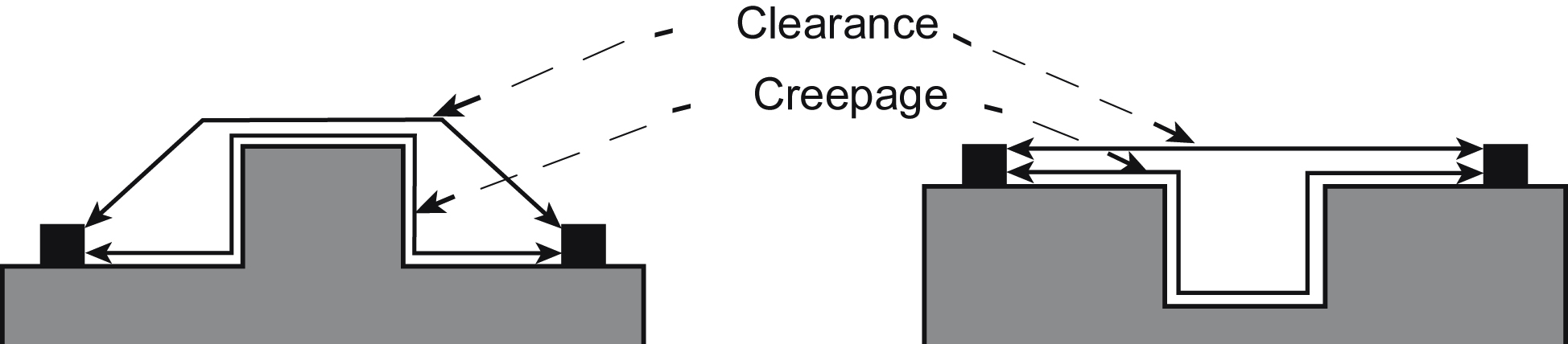
When two nonconductive materials are rubbed together, electrons from one material are transferred to the other. This results in the accumulation of triboelectric charge on the surface of the material. The amount of the charge caused by movement of the materials is a function of the separation of the materials in the triboelectric series, an example of which is shown in Fig. 9.3. Additional factors are the closeness of contact, rate of separation, and humidity. Fig. 8.3 shows the electrostatic voltage related to materials and humidity, from which you can see that possible voltages can exceed 10 kV.
If this charge is built up on the human body, as a result of natural movements, it can then be discharged through a terminal of an electronic component. This will damage the component at quite low thresholds, easily less than 1 kV, depending on the device. Of the several contributory factors, low humidity is the most severe; if relative humidity is higher than 65% (which is frequent in maritime climates such as the UK's) then little damage is likely. Lower than 20%, as is common in continental climates such as the United States, is much more hazardous.
Gate-oxide breakdown of MOS or CMOS components is the most frequent, though not the only, failure mode. Static-damaged devices may show complete failure, intermittent failure, or degradation of performance. They may fail after one very high voltage discharge or because of the cumulative effect of several discharges of lower potential.
Static Protection
To protect against ESD damage, you need to prevent static buildup and to dissipate or neutralize existing charges. At the same time, operators (including yourself and your design colleagues) need to be aware of the potential hazard. The methods used to do this include the following:
• Package-sensitive devices or assemblies in conductive containers, keep them in these until use, and ensure they are clearly marked.
• Remove nonconductive items such as polystyrene cups, synthetic garments, wrapping film, etc. from the work area.
• Ground the assembly operator through a wrist strap, in series with a 1-MΩ resistor for electric shock protection.
• Ground soldering tool tips.
• Use ionized air to dissipate charge from nonconductors, or maintain a high relative humidity.
• Create and maintain a static-safe work area where these practices are adhered to.
• Ensure that all operators are familiar with the nature of the ESD problem.
• Mark areas of the circuit where a special ESD hazard exists; design circuits to minimize exposed high-impedance or unprotected nodes.
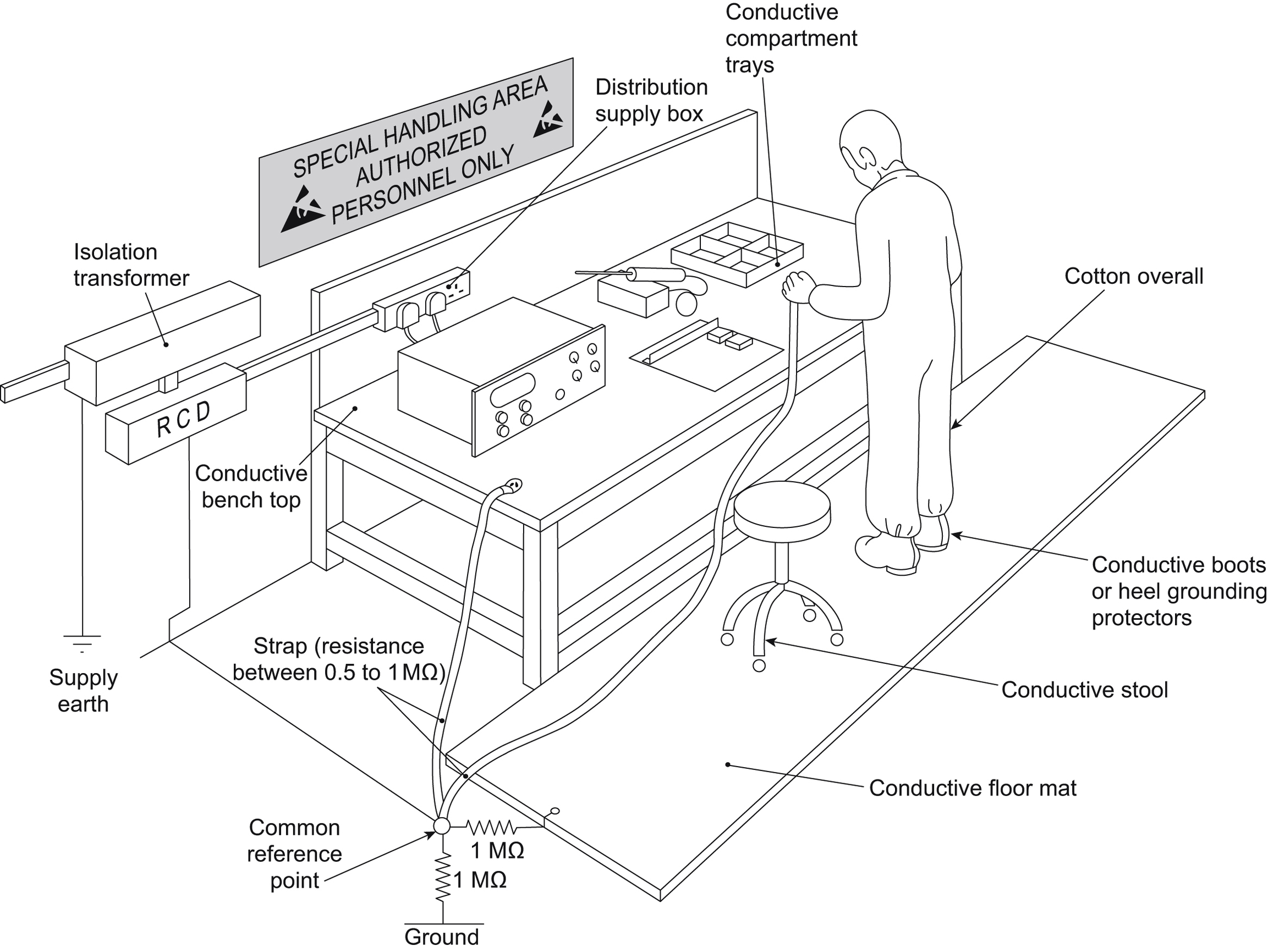
All production assembly areas should be divided into static-safe workstation positions. Your design and development prototyping lab should also follow these precautions, since it is quite possible to waste considerable time tracking down a fault in a prototype, which is due to a static-damaged device. A typical static-safe area layout is shown in Fig. 9.4. BS CECC 00015: Part 1:1991 gives a code of practice for the handling of electrostatic sensitive devices.
9.4. Testability
The previous section's checklist included some items that referred to the testability of the design. It is vital that you give sufficient thought throughout the design of the product as to how the assembled unit or units will be tested to prove their correct function. In the very early stages, you should already know whether your test department will be using in-circuit testing, manual functional testing, functional testing on ATE, boundary scan, or a combination of these methods. You should then be in a position to include test access points and circuits in the design as it progresses. This is a more effective way of incorporating testability than merely bolting it on at the end.
9.4.1. In-Circuit Testing
The first test for an assembled PCB is to confirm that every component on it is correctly inserted, of the right type or value, and properly soldered in. It is quite possible for manual assembly personnel to insert the wrong component, or insert the right one incorrectly polarized, or even to omit a component or series of components. Automatic assembly is supposed to avoid such errors, but it is still possible to load the wrong component into the machine or for components to be marked incorrectly. Automatic soldering has a higher success rate than hand soldering but bad joints due to lead or pad contamination can still occur.
In-circuit testing lends itself to automatic test fixture and test program generation. Each node on the PCB has to be probed, which requires a bed-of-nails test fixture (Fig. 9.5), and this can be designed automatically from the PCB layout data. Similarly, the expected component characteristics between each node can be derived from the circuit schematic, using a component parameter library.

An in-circuit tester carries out an electrical test on each component, to verify its behavior, value, and orientation, by applying voltages to nodes that connect to each component and measuring the resulting current. Interactions with other components are prevented by guarding or back-driving. The technique is successful for discrete components but less so for integrated circuits, whose behavior cannot be described in terms of simple electrical characteristics. It is therefore most widely applied on boards, which contain predominantly discrete components, and which are produced in high volume, as the overhead involved in programming and building the test fixture is significant. It does not of itself guarantee a working PCB. For this, you need a functional test.
9.4.2. Functional Testing
A functional test checks the behavior of the assembled board against its functional specification, with power applied and with simulated or special test signals connected to the input/output lines. It is often combined with calibration and setup adjustments. For low-volume products you will normally write a test procedure around individual test instruments, such as voltmeters, oscilloscopes, and signal generators. You may go so far as to build a special test jig to simulate some signals, interface others, provide monitored power, and make connections to the board under test. The test procedures will consist of a sequence of instructions to the test technician—apply voltage A, observe signal at B, adjust trimmer C for a minimum at D, and so on—along with limit values where measurements are made.
The disadvantage of this approach is that it is costly in terms of test time. This puts up the overhead cost of each board and affects the final cost price of the overall unit. It is cheap as far as instrumentation goes, since you only need a simple test jig, and you will normally expect the test department to have the appropriate lab equipment to hand. Hence it is best suited to low production volumes where you cannot amortize the cost of automatic test equipment.
A further, hidden, disadvantage may be that you do not have to define the testing absolutely rigorously but can rely on the experience of the test technician to make good any deficiencies in the test procedure or measurement limits. It is common for test personnel to develop a better “feel” for the quirks of a particular design's behavior under test than its designer ever could. Procedural errors and invalid test limits may be glossed over by a human tester, and if such information is not fed back to the designer then the opportunity to optimize that or subsequent designs is lost.
Automatic Test Equipment
Functional testing may more easily be carried out by ATE. In this case, the function of the human tester is reduced to that of loading and unloading the unit under test, pressing the “go” button and observing the pass/fail indicator. The testing is comprehensively deskilled; the total unit test time is reduced to a few minutes or less. This minimizes the test cost.
The costs occur instead at the beginning of the production phase, in programming the ATE and building a test fixture. The latter is similar to (in some cases may be identical to) the bed-of-nails fixture which would be used for in-circuit testing (Fig. 9.5). Or, if all required nodes are brought out to test connectors, the test fixture may consist of a jig, which automatically connects a suite of test instrumentation to the board under the command of a computer-based test program. The IEEE-488 standard bus allows interconnection of a desktop computer and remote-controlled meters, signal generators, and other instruments, for this purpose.
The skill required for a test technician now resides in the test program, which may have been written by you as designer or by a test engineer. In any case it needs careful validation before it is let loose on the product, since it does not have the skill or expertise to determine when it is making an invalid test. The cost involved in designing and building the test fixture, programming it, and validating the program and the capital cost of the ATE itself need to be carefully judged against the savings that will be made in test time per unit. It is normally only justified if high production volumes are expected.
9.4.3. Boundary Scan and Joint Test Action Group
Many digital circuits are too complex to test by conventional in-circuit probing. Even if bed-of-nails contact could be made to the hundreds and sometimes thousands of test pads that would be needed, the IC functions and pin states would be so involved that no absolute conclusions could be drawn from the voltage and impedance states recorded. The increased use of small-sized PCBs, with surface mount, fine pitch components installed on both sides, presents the greatest problem. So a different method has been developed to address this problem, and it is known as boundary-scan testing.
History
In 1985, an ad hoc group created the Joint Test Action Group (JTAG). JTAG had over 200 members around the world, including major electronics and semiconductor manufacturers. This group met to establish a solution to the problems of board test and to promote a solution as an industry standard. They subsequently developed a standard for integrating hardware into compliant devices, which could be controlled by software. This was termed boundary-scan testing. The JTAG proposal was approved in 1990 by the IEEE and defined as IEEE Standard 1149.1-1990 Test Access Port and Boundary Scan Architecture. Since the 1990 approval, updates have been published in 1993 as supplement IEEE Std 1149.1a-1993 and in 1995 as IEEE Std 1149.1b-1994.
Description of the Boundary-Scan Method
Boundary scan is a special type of scan path with a register added at every I/O pin on a device. Although this requires special extra test latches on these pins, the technique offers several important benefits, the most obvious being that it allows fault isolation at the component level. A major problem driving the development of boundary scan has been the adverse effect on testability of surface-mount technology. The inclusion of a boundary-scan path in surface-mount components is sometimes the only way to perform continuity tests between devices. By placing a known value on an output buffer of one device and observing the input buffer of another interconnected device, it is easy to check the interconnection of the PCB net. Failure of this simple test indicates broken circuit traces, dry solder joints, solder bridges, or ESD-induced failures in an IC buffer—all common problems on PCBs.
Another advantage of the boundary-scan method is the ability to apply predeveloped functional pattern sets to the I/O pins of the IC by way of the scan path. IC manufacturers and ASIC developers create functional pattern sets for test purposes. Subsets of these patterns can be reused for in-circuit functional IC testing, which can show significant savings on development resources.
Each device to be included within the boundary scan has the normal application-logic section and related input and output, and in addition a boundary-scan path consisting of a series of boundary-scan cells (BSCs), typically one BSC per IC function pin (Fig. 9.6). The BSCs are interconnected to form a shift register scan path between the host IC's test data input (TDI) pin and test data output (TDO) pin. During normal IC operation, input and output signals pass freely through each BSC. However, when the boundary-test mode is entered, the IC's internal logic may be disconnected and its boundary controlled in such a way that test stimuli can be shifted in and applied from each BSC output, and test responses can be captured at each BSC input and shifted out for inspection. External testing of traces and neighboring ICs on a board assembly is achieved by applying test stimuli from the output BSCs and capturing responses at the input BSCs. If required, internal testing of the application logic can be achieved by applying test stimuli from the input BSCs and capturing responses at the output BSCs. The implementation of a scan path at the boundary of IC designs provides an embedded testing capability that can overcome the physical access problems referred to above.

As well as performing boundary tests of each IC, ICs may also be instructed via the scan path to perform a built-in self-test operation, and the results inspected via the same path. Boundary scan is not limited to individual ICs; several ICs on a board will normally be linked together to offer an extended scan path (which could be partitioned or segmented to optimize testing speed). The whole board itself could be regarded as the system to be tested, with a scan path encompassing the connections at the board's boundary, and BSCs implemented at these connections using ICs designed for the purpose.
Devices
Every IEEE Std 1149.1-compatible device has four additional pins—two for control and one each for input and output serial test data. These are collectively referred to as the “test access port” (TAP). To be compatible, a component must have certain basic test features, but the standard allows designers to add test features to meet their own unique requirements. A JTAG-compliant device can be a microprocessor, microcontroller, programmable logic device, complex programmable logic device, field programmable gate array, ASIC, or any other discrete device that conforms to the 1149.1 specification. The TAP pins are:
• TCK—Test clock input. Shift register clock separate from the system clock.
• TDI—Data is shifted into the JTAG-compliant device via TDI.
• TDO—Data is shifted out of the device via TDO.
• TMS—Test mode select. TMS commands select test modes as defined in the JTAG specification.
The 1149.1 specification stipulates that at every digital pin of the IC, a single cell of a shift-register is designed into the IC logic. This single cell, known as the BSC, links the JTAG circuitry to the IC's internal core logic. All BSCs of a particular IC constitute the boundary-scan register (BSR), whose length is of course determined by the number of I/O pins that IC has. BSR logic becomes active when performing JTAG testing, otherwise it remains passive under normal IC operation. A 1-bit bypass register is also included to allow testing of other devices in the scan path.
You communicate with the JTAG-compliant device using a hardware controller that either inserts into a PC add-in card slot or by using a stand-alone programmer. The controller connects to the TAP on a JTAG-compliant PCB—which may be the port on a single device, or it may be the port created by linking a number of devices. You (or your test department) then must write the software to perform boundary-scan programming and testing operations.
As well as testing, the boundary-scan method can be used for various other purposes that require external access to a PCB, such as flash memory programming.
Deciding Whether or Not to Use Boundary Scan
Although the boundary-scan method has enormous advantages for designers faced with the testing of complex, tightly packed circuits, it is not without cost. There is a significant logic overhead in the ICs as well as a small overhead on the board in implementing the TAP, and there is the need for your test department to invest in the resources and become familiar with the method as well as programming each product. As a rough guide, you can use the following rule2 (relating to ASIC design) to decide on whether or not the extra effort will be cost-effective:
• Designs with fewer than 10-K gates: not generally complex enough to require structured test approaches. The overhead impact is usually too high to justify them. Nonstructured, good design practices are usually sufficient.
• Designs with more than 10-K gates, but fewer than 20-K gates: Structured techniques should be considered for designs in this density. Nonstructured, good design practices are probably sufficient for highly combinatorial circuits without memory. Structured approaches should be considered as complexity is increased by the addition of sequential circuits, feedback, and memory. Consider boundary-scan testing for reduced cycle times and high fault grades.
• Designs with more than 20-K gates: The complexity of circuits this dense usually requires structured approaches to achieve high fault grades. At this density, it is often hard to control or observe deeply embedded circuits. The overhead associated with structured testability approaches is acceptable.
9.4.4. Design Techniques
There are many ways in which you can design a PCB circuit to make it easy to test, or conversely hard to test. The first step is to decide how the board will be tested, which is determined by its complexity, expected production volume, and the capabilities of the test department.
Bed-of-Nails Probing
If you will be using a bed-of-nails fixture, then the PCB layout should allow this. Leave a large area around the outside of the board, and make sure there are no unfilled holes, to enable a good vacuum pressure to be developed to force the board onto the probes. Or if the board will be clamped to the fixture, make sure there is space on the top of the board for the clamps. Decide where your test nodes need to be electrically, and then lay out the board to include target pads on the underside for the probes. These pads should be spaced on a 0.1″ (2.5 mm) grid for accurate drilling of the test jig; down to 0.05″ or 1 mm is possible if the board layout is tight. It is not good practice to use component lead pads as targets, since pressure from the probe may cause a defective joint to appear good. Ensure that tooling holes are provided and are accurately aligned with the targets.
Remember that a bed-of-nails jig will connect several long, closely coupled wires to many nodes in the circuit. This will severely affect the circuit's stray reactances, and thereby modify its high frequency response. It is not really suitable for functionally testing high-frequency or high-speed digital circuits.
Test Connections
If your test department does not want to use bed-of-nails probing, then help them find the test points that are necessary by bringing them out to test connectors. These can be cheap-and-cheerful pin strips on the board since they will normally only be used once. The matching test jig can then take signals from these connections direct to the test instrumentation via a switch arrangement. Of course, preexisting connectors such as multiway or edge connectors can be used to bring out test signals on unused pins. Be careful, though, that you do not bring long test tracks from one side of the board to the other and thereby compromise the circuit's cross talk, noise susceptibility, and stability. Extra local test connectors are preferable.
Circuit Design
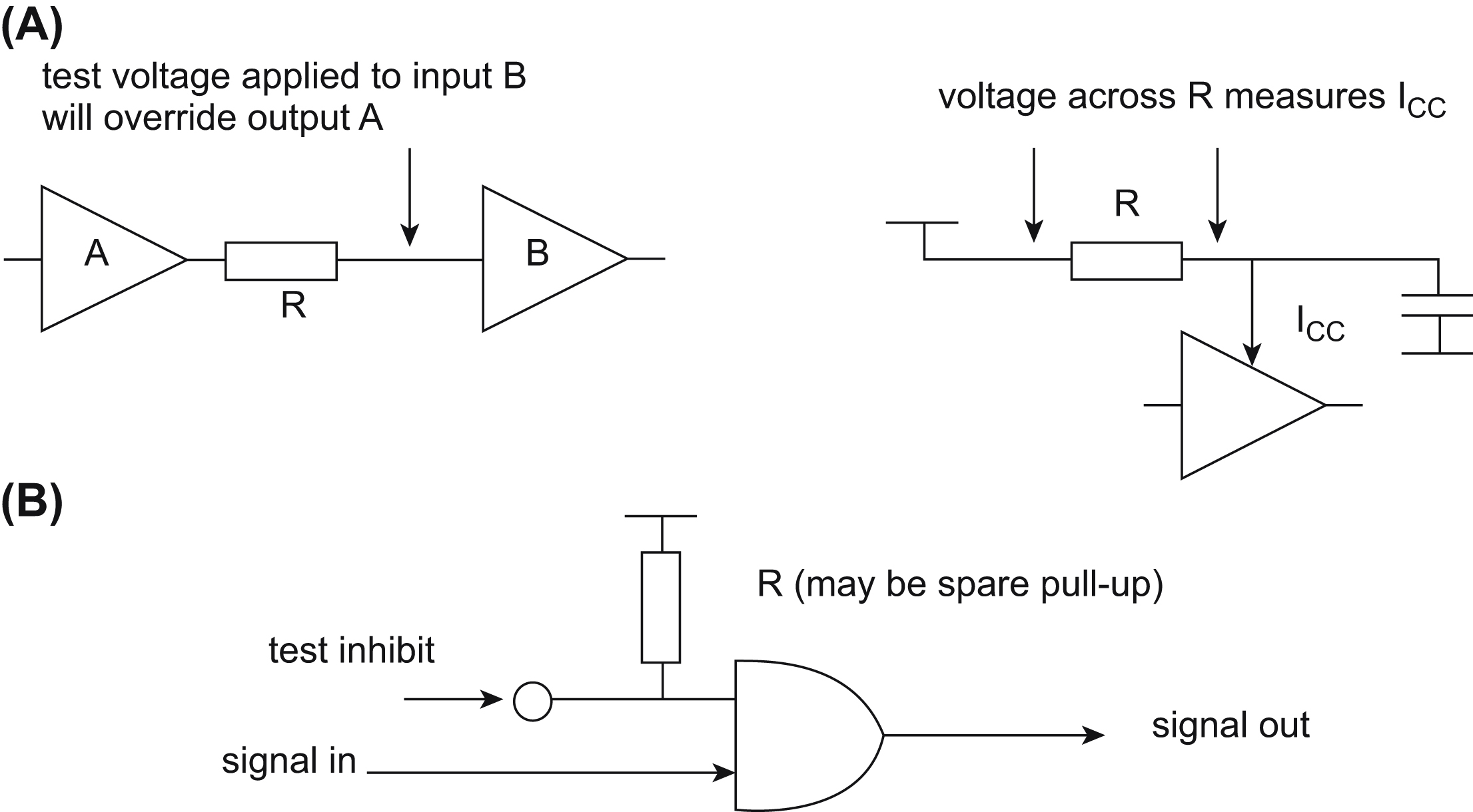
There are many design tricks to make testing easier. A simple one is to include a series resistor in circuits where you will want to back-drive against an output, or where you will want to measure a current (Fig. 9.7A). The cost of the resistor is minimal compared to the test time it might save. Of course, you must ensure that the resistor does not affect normal circuit operation. Also, unused digital gate inputs may be taken to a pull-up resistor rather than direct to supply or ground (cf. Section 6.1.5), and this point can then be used to inhibit or enable logic signals for testing purposes only (Fig. 9.7B).
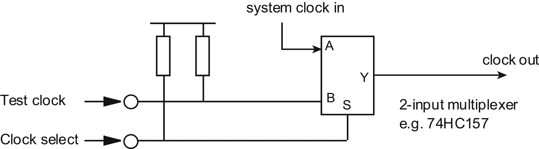
The theme of Fig. 9.7B can be taken further to incorporate extra logic switching to allow data or timing signals to be derived either from the normal on-board source or from the external test equipment. This is particularly useful in situations where testing logic functions from the normal system clock would result either in too fast operation, or too slow. The clock source can be taken through a 2-input data multiplexer such as the 74HC157, one input of which is taken via a test connector to the external clock as shown in Fig. 9.8. In normal operation the clock select and test clock inputs are left unconnected, and the system clock is passed directly through the multiplexer.
When you are considering testing a microprocessor board, it is advantageous to have a small suite of test software resident on the main program PROM. This can be activated on start-up by reading a digital input, which is connected to a test link or test probe. If the test input is set, the program jumps to the test routines rather than to the main operating routines. These are arranged to exercise all inputs, outputs, and control signals continuously in a predictable manner, so that the test equipment can monitor them for the correct function. The test software operation depends of course on the core functions of the microprocessor, and its bus and control signal interconnections, being fault free.
More complex digital systems cannot easily be tested or, more to the point, debugged, with the techniques described so far. The boundary-scan methods described in Section 9.3.3 are aimed at these applications, and you need to design them in from the start, since they consume a serious amount of circuit overhead to function.
9.5. Reliability
The reliability of electronic equipment can, to some extent, be quantified, and a separate discipline of reliability engineering has grown up to address it. This section will serve as an introduction to the subject for those designers who are not fortunate enough to have a reliability engineering department at their disposal.
9.5.1. Definitions
Reliability, itself, has a strictly defined meaning. This can be stated as “the probability that a system will operate without failure for a specified period, subject to specified environmental conditions.” Thus it can be quoted as a single number, such as 90%, but this is subject to three qualifications:
• agreement as to what constitutes a “failure.” Many systems may “fail” without becoming totally useless in the process.
• a specified operating lifetime. No equipment will operate forever; reliability must refer to the reasonably foreseen operating life of the equipment, or to some other agreed period. The age of the equipment, which may well affect failure rate, is not a factor in the reliability specification.
• agreement on environmental conditions. Temperature, moisture, corrosive atmospheres, dust, vibration, shock, supply, and electromagnetic disturbances all have an effect on equipment operation and reliability is meaningless if these are not quoted.
If you offer or purchase equipment whose reliability is quoted for one set of conditions and it is used under another set, you will not be able to extrapolate the reliability figure to the new conditions unless you know the behavior of those parameters that affect it.
Mean Time Between Failures
For most of the life of a piece of electronic equipment, its failure rate (denoted by λ) is constant. In the early stages of operation it could be high and decrease as weak components fail quickly and are replaced; late in its life components may begin to “wear out” or corrosion may take its toll, and the failure rate may start to rise again. The reciprocal of failure rate during the constant period is known as the mean time between failures (MTBFs). This is generally quoted in hours, while failure rate is quoted in faults per hour. For instance, an MTBF of 10,000 h is equivalent to a failure rate of 0.0001 faults per hour or 100 faults per 106 h. MTBF has the advantage that it does not depend on the operating period and is therefore more convenient to use than reliability.
Mean Time to Failure
MTBF measures equipment reliability on the assumption that it is repaired on each failure and put back into service. For components that are not repairable, their reliability is quoted as mean time to failure (MTTF). This can be calculated statistically by observing a sample from a batch of components and recording each one's working life, a procedure known as life testing. The MTTF for this batch is then given by the mean of the lifetimes.
Availability
System users need to know for what proportion of time their system will be available to them. This figure is given by the ratio of “uptime” (U), during which the system is switched on and working, to total operating time. The difference between the two is the “downtime” (D) during which the system is faulty and/or under repair. Therefore we can define the availability, A, using Eq. (9.1):
The availability (A) can also be related to the MTBF figure and the mean time to repair (MTTR) figure by Eq. (9.2)
The availability of a particular system can be monitored by logging its operating data, and this can be used to validate calculated MTBF and MTTR figures. It can also be interpreted as a probability that at any given instant the system will be found to be working.
9.5.2. The Cost of Reliability
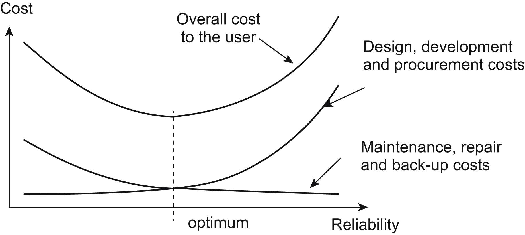
Reliability does not come for free. Design and development costs escalate as more effort is put into assuring it, and component costs increase if high performance is required of them. For instance, it would be quite possible to improve the reliability of, say, an audio power amplifier by using massively overrated output transistors, but these would add considerably to the selling cost of the amplifier. On the other hand, if the selling cost were reduced by specifying underrated transistors, the users would find their total operating costs mounting since the output transistors would have to be replaced more frequently. Thus there is a general trend of decreasing operating or “life-cycle” costs and increasing unit costs, as the designed-in reliability of a given system increases. This leads to the notion of an “optimum” reliability figure in terms of cost for a system. Fig. 9.9 illustrates this trend. The criterion of good design is then to approach this optimum as closely as possible.
Of course, this argument only applies when the cost of unreliability is measured in strictly economic terms. Safety-critical systems, such as nuclear or chemical process plant controllers, railway signaling or flight-critical avionics, must instead meet a defined reliability standard, and the design criterion then becomes one of assuring this level of reliability, with cost being a secondary factor.
9.5.3. Design for Reliability
The goal of any circuit designer is to reduce the failure rate of his or her design to the minimum achievable within cost constraints. The factors that help in meeting this goal include the following:
• Use effective thermal management to minimize temperature rise.
• Derate susceptible components as far as possible.
• Specify high reliability or quality-assured components.
• Specify stress screening or burn-in tests.
• Keep circuits simple, and use the minimum number of components.
• Use redundancy techniques at the component level.
Temperature
High temperature is the biggest enemy of all electronic components and measures to keep it down are vital. Temperature rise accelerates component breakdown because chemical reactions occurring within the component, which govern bond fractures, growth of contamination or other processes, have an increased rate of reaction at higher temperature. The rate of reaction is determined by the Arrhenius equation,
where λ gives a measure of failure rate; K is a constant depending on the component type; E is the reaction's activation energy; k is Boltzmann's constant, 1.38 × 10⁻²³ J/K; T is absolute temperature.
Many reactions have activation energies around 0.5 eV, which results in an approximate doubling of λ with every 10°C rise in temperature, and this is a useful rule of thumb to apply for the decrease in reliability versus temperature of typical electronic equipment with many components. Some reactions have higher activation energy, which give a faster increase of λ with temperature.
Thermal management itself is covered in Section 9.5.
Derating
There is a very significant improvement to be gained by operating a component well within its nominal rating. For most components this means either its voltage or power rating, or both.
Take capacitors as an example. Conventionally, you will determine the maximum dc bias voltage a capacitor will have to withstand under worst-case conditions, and then select the next highest rating. Overspecifying the voltage rating may result in a larger and more costly component.
However, capacitor life tests show that as the maximum working voltage is approached, the failure rate increases as the fifth power of the voltage. Therefore, if you run the capacitor at half its rated voltage, you will observe a failure rate 32 times lower than if it is run at full-rated voltage. Given that a capacitor of double the required rating will not be as much as double the size, weight or cost, except at the extremes of range, the improvement in reliability is well worth having.
In many cases there is no difficulty in using a derated capacitor; small film capacitors for instance are rated at a minimum of 50 or 100 V and are frequently used in 5-V circuits. Electrolytics on the other hand are more likely to be run near their rating. These capacitors already have a much higher failure rate than other types because of their construction—the electrolyte has a tendency to “dry out,” especially at high temperatures—and so you will achieve significant improvement, albeit at higher cost, if you heavily derate them.
Derating the power dissipation of resistors reduces their internal temperature and therefore their failure rate. In low-voltage circuits there is no need to check power rating for any except low-value parts; if for instance you use 0.4-W metal film resistors in a circuit with a maximum supply of 10 V, you can be sure that all resistors over 500 Ω will be derated by at least a factor of 2, which is normally enough.
Semiconductor devices are normally rated for power, current, and voltage, and derating on all of these will improve failure rate. The most important are power dissipation, which is closely linked to junction temperature rise and cooling provision, and operating voltage, especially in the presence of possible transient overvoltages.
High Reliability Components
Component manufacturers' reputations are seriously affected by the perceived reliability or otherwise of their product, so most will go to considerable effort not to ship defective parts. However, the cost of detecting and replacing a faulty part rises by an order of magnitude at each stage of the production process, starting at goods inwards inspection, proceeding through board assembly, test and final assembly, and ending up with field repair. You may therefore decide (even in the absence of mandatory procurement requirements on the part of your customer) that it is worth spending extra to specify and purchase parts with a guaranteed reliability specification at the “front end” of production.
CENELEC Electronic Components Committee
Initially it was military requirements, where reliability was more important than cost that drove forward schemes for assessed quality components. More recently many commercial customers have also found it necessary to specify such components. The need for a common standard of assessed quality is met in Europe by the CECC3 scheme. This has superseded the earlier national BS9000 series of standards. CECC documents refer to a “harmonized system of quality assessment for electronic components.”
Generic specifications are found in the CECC series for all types of component, which are covered by the scheme. These specify physical, mechanical, and electrical properties, and lay down test requirements. Individual component specifications are not found under the scheme.
Stress Screening and Burn-In
These specifications all include some degree of stress screening. This phrase refers to testing the components under some type of stress, typically at elevated temperature, under vibration or humidity and with maximum rated voltage applied, for a given period. This practice is also called “burning in.” The principle is that weak components will fail early in their life and the failures can be accelerated by operating them under stress. These can then be weeded out before the parts are shipped from the manufacturer. A typical test might be 160 h at 125°C. Another common test is a repeated temperature cycle between the extremes of the permitted temperature range, which exposes failures due to poor bonding or other mechanical faults.
Such stress screening can be applied to any component, not just semiconductors, and also to entire assemblies. If you are unsure of the probable quality of early production output of a new design, specifying stress screening on the first few batches is a good way to discover any recurrent production faults before they are passed out to the customer. It is expensive in time, equipment, and inventory and should not be used as a crutch to compensate for poor production practices. It should only be employed as standard if the customer is willing to pay for it.
Simplicity
The failure rate of an electronic assembly is roughly equal to the sum of the failure rates of all its components. This assumes that a failure in any one component causes the failure of the whole assembly. This is not necessarily a valid assumption, but to assume otherwise you would have to work out the assembly's failure modes for each component failure and for combinations of failures, which is not practical unless your customer is prepared to pay for a great deal of development work.
If the assumption holds, then reducing the number of components will reduce the overall failure rate. This illustrates a very important principle in circuit design: the highest reliability comes from the simplest circuits. Apply Occam's razor (“entities should not be multiplied beyond necessity”) and cut down the number of components to a minimum.
Redundancy
Redundancy is employed at the system level by connecting the outputs of two or more subsystems together such that if one fails, the others will continue to keep the system working. A typical example might be several power supplies, each connected to the same power distribution rail (via isolating diodes) and each capable of supplying the full load. If the reliability of the interconnection is neglected, the probability of all supplies failing simultaneously is the product of the probabilities of failure of each supply on its own, assuming that a common-mode failure (such as the mains supply to all units going off) is ruled out.
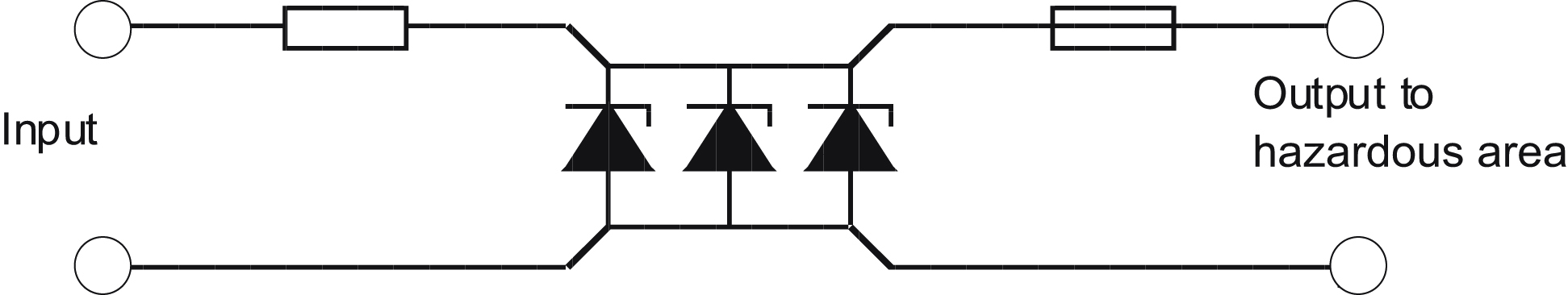
The principle can also be applied at the component level. If the probability of a single component failing is too high then redundant components can be placed in parallel or series with it, depending on the required failure mode. This technique is mandatory in certain fields, such as intrinsically safe instrumentation. Fig. 9.10 illustrates redundant zener diode clamping. The zeners prevent the voltage across their terminals from rising to an unsafe value in the event of a fault voltage being applied at the input to the barrier. One zener alone would not offer the required level of reliability, so two further ones are placed in parallel, so that even with an open-circuit failure of two out of the three, the clamping action is maintained. The interconnections between the zeners must be solid enough not to materially affect the reliability of the combination.
Some provision must normally be made for detecting and indicating a failed component or subsystem so that it can be repaired or replaced. Otherwise, once a redundant part has failed, the overall reliability of the system is severely reduced.
9.5.4. The Value of Mean-Time-Between-Failure Figures
The mean-time-between-failure figure as defined in Section 9.4.1 can be calculated before the equipment is put into production by summing the failure rates of individual components to give an overall failure rate for the whole equipment. As discussed earlier, this assumes that a fault in any one component causes the failure of the whole assembly. This method presupposes adequate data on the expected failure rates of all components that will be used in the equipment.
Such sources of failure rate data for established component types are available. The most widely used is MIL-HDBK-217, now in its fifth revision, published by the United States Department of Defense. This handbook lists failure-rate models and tables for a wide variety of components, based on observed failure measurements. A failure rate for each component can be derived from its operating and environmental conditions, derating factor and method of construction or packaging. A further factor that is included for integrated circuits is their complexity and pinout. Another source of failure rate data, somewhat less comprehensive but widely used for telecommunications applications, is British Telecom's handbook HRD4.
The disadvantage with using such data is that it cannot be up-to-date. Proper failure rate data takes years to accumulate, and so data extracted from these tables for modern components will not be accurate. This is especially true for integrated circuits. Generally, figures based on obsolete failure-rate data will tend to be pessimistic, since the trend of component reliability is to improve.
Calculations of failure rates at component level are tedious, since operating conditions for each component, notably voltage and power dissipation, must be a part of the calculation to arrive at an accurate value. They do lend themselves to computer derivation, and software packages for reliability prediction are readily available. Since in many cases such operating conditions are highly variable, it is arguable that you will not obtain much more than an order-of-magnitude estimate of the true figure anyway.
A published MTBF figure does not tell you how long the unit will actually last, and it does not indicate how well the unit will perform in the field under different environmental and operating conditions. Such figures are mainly used by the marketing department to make the specification more attractive. But MTBF prediction is valuable for two purposes:
• for the designer, it gives an indication of where reliability improvements can most usefully be made. For instance, if as is often the case the electrolytic capacitors turn out to make the highest contribution to overall failure rate, you can easily evaluate the options available to you in terms of derating or adding redundant components. You need not waste effort on optimizing those components which have little effect overall.
• for the service engineer, it gives an idea of which components are likely to have failed if a breakdown occurs. This can be valuable in reducing servicing and repair time.
9.5.5. Design Faults
Before leaving the subject of reliability design, we should briefly mention a very real problem, which is the fallibility of the designers themselves. There is no point in specifying highly reliable components or applying all manner of stress screening tests or redundancy techniques if the circuit is going to fail because it has been wrongly designed. Design faults can be due to inexperience, inattention, or incompetence on the part of the designer, or simply because the project timescale was too short to allow the necessary cross-checking. Computer-aided design techniques and simulators can reduce the risk, but they cannot eliminate the potential for human error completely.
The Design Review
An effective and relatively painless way of guarding against design faults is for your product development department to instigate a system of frequent design reviews. In these, a given designer's circuit is subjected to a peer critique to probe for flaws, which might not be apparent to the circuit's originator. The critique can check that the basic circuit concept is sound and cost effective, that all component tolerances have been accounted for, that parts will not be operated outside their ratings, and so on. The depth of the review is determined by the resources that are available within the group; the reviewers should preferably have no connection with the project being reviewed, so that they are able to question underlying and unstated assumptions. Naturally, the effectiveness of such a system depends on the resources a company is prepared to devote to it, and it also depends on the willingness of the designer to undergo a review. Personality clashes tend to surface on these occasions. Each designer develops pet techniques and idiosyncrasies during their career, and provided these are not actually wrong they should not attract criticism. Nevertheless, design reviews are valuable for testing the strength of a design before it gets to the stage where the cost of mistakes becomes significant.
9.6. Thermal Management
It is in the nature of electronic components to dissipate power while they are operating. Any flow of current through a nonideal component will develop some power within that component, which in turn causes a rise in temperature. The rise may be no more than a small fraction of a degree Celsius when less than a milliwatt is dissipated, extending to several tens or even hundreds of degrees when the dissipation is measured in watts. Since excess temperature kills components, some way must be found to maintain the component-operating temperature at a reasonable level. This is known as thermal management.
9.6.1. Using Thermal Resistance
Heat transfer through the thermal interface is accomplished by one or more of three mechanisms: conduction, convection, and radiation. The attractiveness of thermal analysis to electronics designers is that it can easily be understood by means of an electrical analogue. Visualize the flow of heat as emanating from the component, which is dissipating power, passing through some form of thermal interface and out to the environment, which is assumed to have a constant ambient temperature TA and infinite ability to sink heat. Then the heat source can be represented electrically as a current source; the thermal impedances as resistances; the temperature at any given point is the voltage with respect to 0 V; and thermal inertia can be represented by capacitance with respect to 0 V. The 0-V reference itself does not have an exact thermal analogue, but it is convenient to represent it as 0°C, so that temperature in degree Celsius is given exactly by a potential in volts. All these correspondences are summarized in Table 9.2.
Table 9.2
Thermal and Electrical Equivalences
| Thermal Parameter | Units | Electrical Analogue | Units |
| Temperature difference | °C | Potential difference | Volts |
| Thermal resistance | °C/W | Resistance | Ohms |
| Heat flow | J/s (W) | Current | Amps |
| Heat capacity | J/°C | Capacitance | Farads |
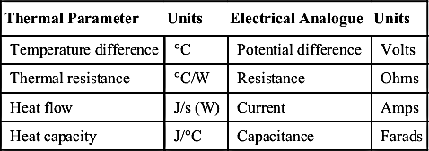
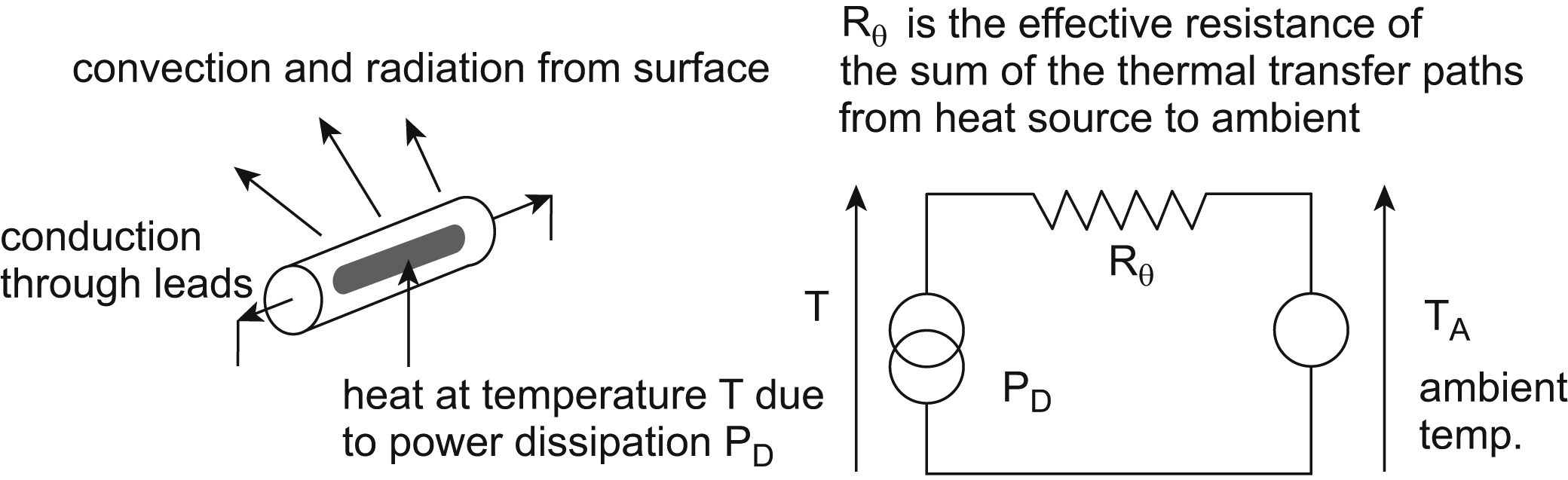
Fig. 9.11 shows the simplest general model and its electrical analogue. The model can be analyzed using conventional circuit theory and yields the following Eq. (9.4) for the temperature at the heat source:
This temperature is the critical factor for electronic design purposes, since it determines the reliability of the component. Reducing any of PD, Rθ, or TA will minimize T. Ambient temperature is not normally under your control but is instead a specification parameter (but see Section 9.5.4). The usual assumption is that the ambient air (or other cooling medium) has an infinite heat capacity, and therefore its temperature stays constant no matter how much heat your product puts into it. The intended operating environment will determine the ambient temperature range, and for heat calculations only the extreme of this range is of interest; the closer this gets to the maximum allowable value of T the harder is your task. Since you are normally attempting to manage a given power dissipation, the only parameter that you are free to modify is the thermal resistance Rθ. This is achieved by heat sinking.
There are more general ways of analyzing heat flow and temperature rise, using thermal conductivity and the area involved in the heat transfer. However, component manufacturers normally offer data in terms of thermal resistance and maximum permitted temperature, so it is easiest to perform the calculations in these terms.
Partitioning the Heat Path
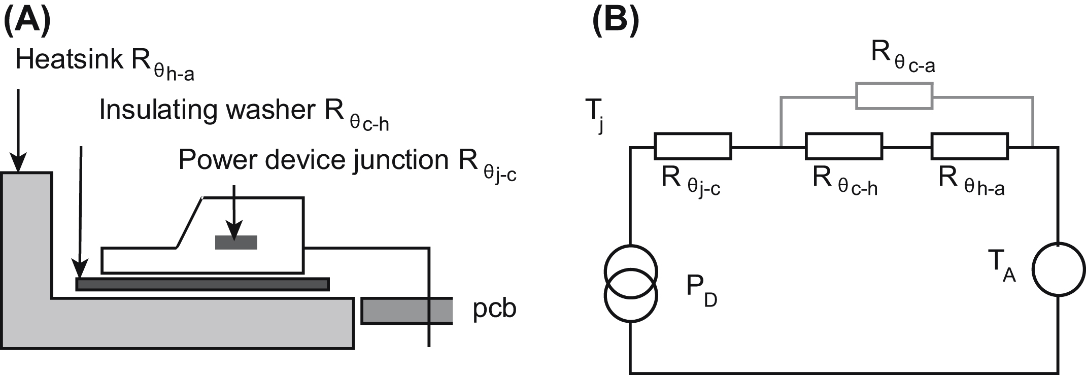
When you have data on the component's thermal resistance directly to ambient, and your mounting method is simple, then the basic model of Fig. 9.11 is adequate. For components that require more sophisticated mounting and whose heat transfer paths are more complicated, you can extend the model easily. The most common application is the power semiconductor mounted via an insulating washer to a heat sink (Fig. 9.12A).
The equivalent electrical model is shown in Fig. 9.12B. Here, Tj is the junction temperature and Rθj−c represents the thermal resistance from junction to case of the device. All manufacturers of power devices will include Rθj−c in their data sheets, and it can often be found in low-power data as well. Sometimes it is disguised as a power derating figure, expressed in W/°C. The maximum allowable value of Tj is published in the maximum ratings section of each data sheet, and this is the parameter that your thermal calculations must ensure is not exceeded.
Rθc−h and Rθh−a are the thermal resistances of the interface between the case and the heat sink, and of the heat sink to ambient, respectively. Rθc−a represents the thermal resistance due to convection directly from case to ambient and can be neglected if you are using a large heat sink.
An example should help to make the calculation clear.
An IRF640 power MOSFET dissipates a maximum of 35 W steady state. It is mounted on a heat sink with a specified thermal resistance of 0.5°C/W, via an insulating pad with a thermal resistance of 0.8°C/W. The maximum ambient temperature is 70°C. What will be the maximum junction temperature?
From the above conditions, Rθc−h + Rθh−a = 1.3°C/W. The IRF640 data quotes a junction-to-case thermal resistance (Rθj−c) of 1.0°C/W.
So the junction temperature is defined by Eq. (9.5):
This is just over the maximum permitted junction temperature of 150°C so reliability is marginal, and you need a bigger heat sink. However, we have neglected the junction-to-ambient thermal resistance, quoted at 80°C/W. This is in parallel with the other thermal resistances. If it is included, the calculation becomes
which is a very minor improvement and not enough to rely on!
This example illustrates a common misconception about power ratings. The IRF640 is rated at 125 W dissipation, yet even with a fairly massive heat sink (0.5°C/W will require a heat sink area of around 80 square inches) it cannot safely dissipate more than 35 W at an ambient of 70°C. The fact is that the rating is specified at 25°C case temperature; higher case temperatures require derating because of the thermal resistance from junction to case. You will not be able to maintain 25°C at the case under any practical application conditions, except possibly outside in the Arctic. Power device manufacturers publish derating curves in their data sheets: rely on these rather than the absolute maximum power rating on the front of the specification.
Incidentally, if having followed these thermal design steps you find that the needed heat sink is too large or bulky, it will be far cheaper to reduce the thermal resistance of the total system. You do this by using two (or more) transistors in parallel in place of a single device. Although the thermal resistances for each of the transistors stay the same, the resultant heat flow for each is effectively halved because each transistor is only dissipating half the total power, and therefore the junction temperature rise is also half.
Thermal Capacity
The previous analysis assumed a steady-state heat flow, in other words constant power dissipation. If this is not a good description of your application, you may need to take account of the thermal capacity of the heat sink. The electrical analogue circuit of Fig. 9.12 can be modified according to Fig. 9.13:
From this you can see that a step increase in dissipated power will actually cause a gradual rise in heat sink temperature Th. This will be reflected at Tj, modified by Rθj−c and Rθc−h, which will take typically several minutes, possibly hours, to reach its maximum temperature. The value of Ch depends on the mass of heat sink metal, and its heat storage capacity. Values of this parameter for common metals are given in Table 9.3. As an example, a 1°C/W aluminum heat sink might have a volume of 120 cm3, which has a heat capacity of 296 J/°C. Multiplying the thermal resistance by the heat capacity gives an idea of the time constant, of 296 s.
The thermal capacity will not affect the end-point steady-state temperature, only the time taken to reach it. But if the heat input is transient, with a low duty cycle to allow plenty of cooling time, then a larger thermal capacity will reduce the maximum temperatures Th and Tj reached during a heat pulse. You can analyze this if necessary with the equivalent circuit of Fig. 9.13. Strictly, the other heat transfer components also have an associated thermal capacity, which could be included in the analysis if necessary.
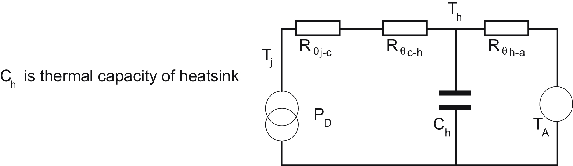
Table 9.3
Thermal Properties of Common Metals
| Metal | Finish | Heat Capacity (J/cm3/°C) | Bulk Thermal Conductivity (W/°C/m) | Surface Emissivity ε (Black Body = 1) |
| Aluminum | Polished | 2.47 | 210 | 0.04 |
| Unfinished | 0.06 | |||
| Painted | 0.9 | |||
| Matt anodized | 0.8 | |||
| Copper | Polished | 3.5 | 380 | 0.03 |
| Machined | 0.07 | |||
| Black oxidized | 0.78 | |||
| Steel | Plain | 3.8 | 40–60 | 0.5 |
| Painted | 0.8 | |||
| Zinc | Gray oxidized | 2.78 | 113 | 0.23–0.28 |

Transient Thermal Characteristics of the Power Device
In applications where the power dissipated in the device consists of continuous low duty cycle periodic pulses, faster than the heat sink thermal time constant, the instantaneous or peak junction temperature may be the limiting condition rather than the average temperature. In this case you need to consult curves for transient thermal resistance. These curves are normally provided by power semiconductor manufacturers in the form of a correction factor that multiplies Rθj−c to allow for the duty cycle of the power dissipation. Fig. 9.13 shows a family of such curves for the IRF640. Because the period for most pulsed applications is much shorter than the heat sink's thermal time constant, the values of Rθh−a and Rθc−h can be multiplied directly by the duty cycle. Then the junction temperature can now be calculated from Eq. (9.7)
where δ is the duty cycle, and K is derived from curves as in Fig. 9.14 for a particular value of δ. PDmax is still the maximum power dissipated during the conduction period, not the power averaged over the whole cycle. At frequencies greater than a few kHz, and duty cycles more than 20%, cycle-by-cycle temperature fluctuations are small enough that the peak junction temperature is determined by the average power dissipation, so that K tends toward δ.

Some applications, notably RF amplifiers or switches driving highly inductive loads, may create severe current crowding conditions on the semiconductor die, which invalidate methods based on thermal resistance or transient thermal impedance. Safe operating areas and di/dt limits must be observed in these cases.
9.6.2. Heat Sinks
As the previous section implied, the purpose of a heat sink is to provide a low thermal resistance path between the heat source and the ambient. Strictly speaking, it is the ambient environment that is the heat sink; what we conventionally refer to as a heat sink is actually only a heat exchanger. It does not itself sink the heat, except temporarily. In most cases the ambient sink will be air, though not invariably: this author recalls one somewhat tongue-in-cheek design for a 1-kW-rated audio amplifier, which suggested bolting the power transistors to a central heating radiator with continuous water cooling! Some designs with a very high power density need to adopt such measures to ensure adequate heat removal.
A wide range of proprietary heat sinks is available from many manufacturers. Several types are predrilled to accept common power device packages. All are characterized to give a specification figure for thermal resistance, usually quoted in free air with fins vertical. Unless your requirements are either very specialized or very high volume, it is unlikely to be worth designing your own heat sink, especially as you will have to go through the effort of testing its thermal characteristics yourself. Custom heat sink design is covered in the application notes of several power-device manufacturers.
A heat sink transfers heat to ambient air primarily by convection and to a lesser degree by radiation. Its efficiency at doing so is directly related to the surface area in contact with the convective medium. Thus heat sink construction seeks to maximize surface area for a given volume and weight; hence the preponderance of finned designs. Orientation of the fins is important because convection requires air to move past the surface and become heated as it does so. As air is heated it rises. Therefore the best convective efficiency is obtained by orienting the fins vertically to obtain maximum air flow across them; horizontal mounting reduces the efficiency by up to 30%.
Convection cooling efficiency falls at higher altitudes. Atmospheric pressure decreases at a rate of 1 mb per 30 ft height gain, from a sea level standard pressure of 1013 mb. Since the heat transfer properties are proportional to the air density, this translates to a cooling efficiency reduction as shown in Table 9.4.

The most common material for heat sinks is black anodized aluminum. Aluminum offers a good balance between cost, weight, and thermal conductivity. Black anodizing provides an attractive and durable surface finish and also improves radiative efficiency by 10–15 times over polished aluminum. Copper can be used as a heat sink material when the optimum thermal conductivity is required, but it is heavier and more expensive.
The cooling efficiency does not increase linearly with size, for two principal reasons:
• longer heat sinks (in the direction of the fins) will suffer reduced efficiency at the end where the air leaves the heat sink, since the air has been heated as it flows along the surface;
• the thermal resistance through the bulk of the metal creates a falling temperature gradient away from the heat source, which also reduces the efficiency at the extremities; this resistance is not included in the simple model of Fig. 9.12.
The first of the above reasons means that it is better to reduce the thermal resistance by making a shorter, wider heat sink than by a longer one. The average performance of a typical heat sink is linearly proportional to its width in the direction perpendicular to the air flow and approximately proportional to the square root of the fin length in the direction parallel to the flow.
Also, the thermal resistance of any given heat sink is affected by the temperature differential between it and the surrounding air. This is due to both increased radiation (see below) and increased convection turbulence as the temperature difference increases. This can lead to a drop in Rθh−a at 20°C difference to 80% of the value at 10°C difference. Or put the other way around, the Rθh−a at 10°C difference may be 25% higher than that quoted at 20°C difference.
Forced Air Cooling
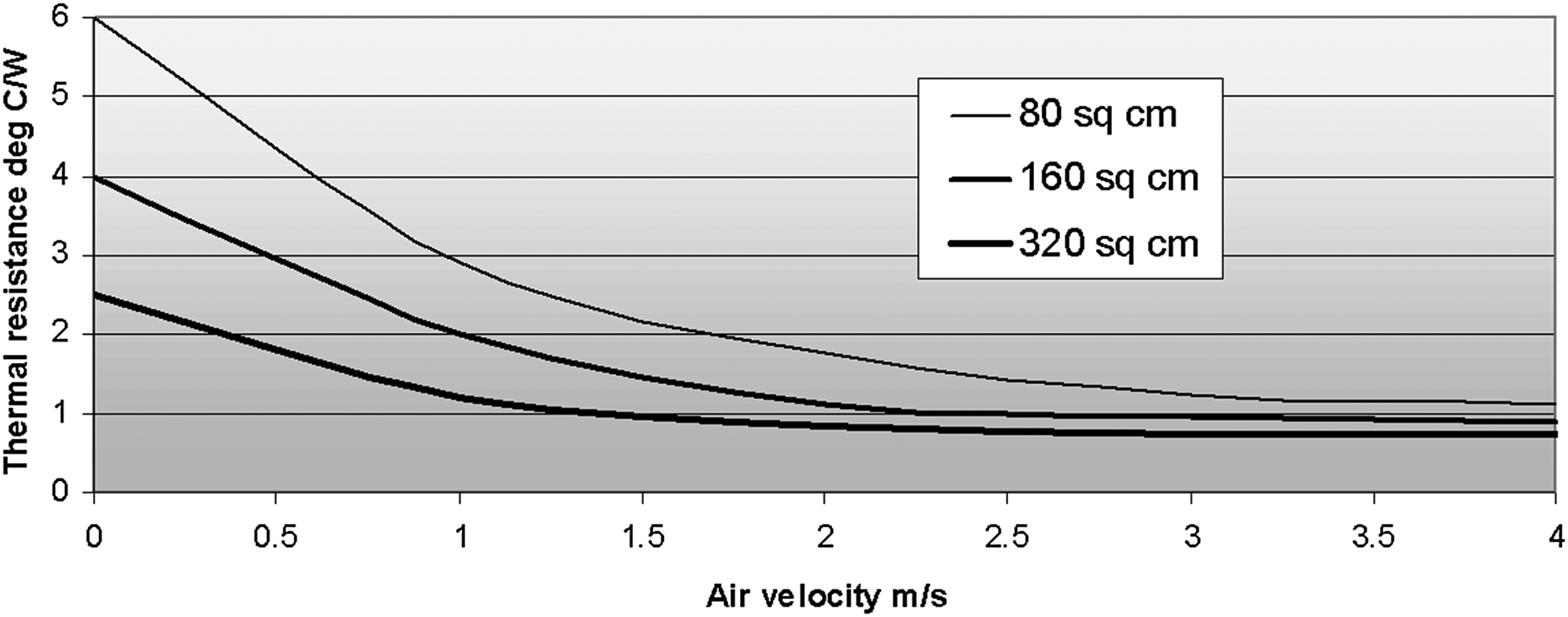
Convective heat loss from a heat sink can be enhanced by forcing the convective medium across its surface. Detailed design of forced air-cooled heat sinks is best done empirically. Simulation software is available to map heat flow and the resulting thermal transfer in complex assemblies; most heat sink applications will be too involved for simple analytical methods to give better than ballpark results. It is not too difficult to use a thermocouple to measure the temperature rise of a prototype design with a given dissipation, most easily generated by a power resistor attached to a dc supply.
Fig. 9.15 shows the improvement in thermal resistance that can be gained by passing air over a square flat plate, and of course at least a similar magnitude can be expected for any finned design. Optimizing the placement of the fins requires either experimentation or simulation, although staggering the fins will improve the heat transfer. When you use forced air cooling, radiative cooling becomes negligible, and it is not necessary to treat the surface of the heat sink to improve radiation; unfinished aluminum will be as effective as black anodized.
Another common use of forced air cooling is ventilation of a closed equipment cabinet by a fan. The capacity of the fan is quoted as the volumetric flow rate in cubic feet per minute (CFM) or cubic meters per hour (1 CFM = 1.7 m3/h). The volumetric flow rate required to limit the internal temperature rise of an enclosure in which PD watts of heat is dissipated to θ°C above ambient is defined by Eq. (9.8):
where ρ is the density of the medium (air at 30°C and atmospheric pressure is 1.3 kg/m3); c is the specific heat capacity of the medium (air at 30°C is around 1000 J/kg°C).
Fan performance is shown as volumetric flow rate versus pressure drop across the fan. The pressure differential is a function of the total resistance to air flow through the enclosure, presented by obstacles such as air filters, louvers, and PCBs. You generally need to derive pressure differential empirically for any design with a nontrivial air-flow path.
Radiation
Radiative cooling is something of a mixed blessing. Radiant heat travels in line of sight and is therefore as likely to raise the temperature of other components in an assembly as to be dissipated to ambient. For the same reason, radiation is rarely a significant contribution to cooling by a finned heat sink, since the finned areas that make up most of the surface merely heat each other. However, radiation can be used to good effect when a clear radiant path to ambient can be established, particularly for high-temperature components in a restricted air flow. The thermal loss through radiation is defined in Eq. (9.9)
where ε is the emissivity of the surface, compared to a black body; ΔT is the temperature difference between the component and environment; Q is given in watts per second per square centimeter.
Emissivity depends on surface finish as well as on the type of material, as shown in Table 9.4. Glossy or shiny surfaces are substantially worse than matt surfaces, but the actual color makes little difference. What is important is that the surface treatment should be as thin as possible, to minimize its effect on convection cooling efficiency.
Poor radiators are also poor absorbers, so a shiny surface such as aluminum foil can be used to protect heat-sensitive components from the radiation from nearby hot components. The reverse also holds, so for instance it is good practice to keep external heat sinks out of bright sunlight.
9.6.3. Power Semiconductor Mounting
The way in which a power device package is mounted to its heat sink affects both actual heat transfer efficiency and long-term reliability. Faulty mounting of metal-packaged devices mainly causes unnecessarily high junction temperature, shortening device lifetime. Plastic packages (such as the common TO-220 outline) are much more susceptible to mechanical damage, which allows moisture into the case and can even crack the semiconductor die.
The factors that you should consider when deciding on a mounting method are summarized in Fig. 9.16 for a typical plastic-packaged device.
Heat Sink Surface Preparation
The heat sink should have a flatness and finish comparable to that of the device package. The higher the power dissipation, the more attention needs to be paid to surface finish. A finish of 50–60 microinches is adequate for most purposes. Surface flatness, which is the deviation in surface height across the device-mounting area, should be less than 4 mils (0.004″) per inch.

The mounting hole(s) should only be large enough to allow clearance of the fastener, plus insulating bush if one is fitted. Too large a hole, if the screw is torqued too tightly, will cause the mounting tab to deform into the hole. This runs the risk of cracking the die, as well as lifting the major part of the package, which is directly under the die off the heat sink in cantilever fashion, seriously affecting thermal transfer impedance. Chamfers on the hole must be avoided for the same reason, but deburring is essential to avoid puncturing insulation material and to maintain good thermal contact. The surface should be cleaned of dust, grease, and swarf immediately before assembly.
Lead Bend
Bending the leads of any semiconductor package stresses the lead interface and can result in cracking and consequent unreliability. If possible, mount your devices upright on the PCB so that lead bending is unnecessary. Plastic-packaged devices (TO220, TO126 etc.) can have their leads bent, provided that
• the minimum distance between the plastic body and the bend is 4 mm
• the minimum bend radius is 2 mm
• maximum bend angle is no greater than 90 degrees
• leads are not repeatedly bent at the same point
• no axial strain is applied to the leads, relative to each other or the package
Use round-nosed pliers or a proper lead-forming jig to ensure that these conditions are met. Metal-cased devices must not have their leads bent, as this is almost certain to damage the glass seal.
When the device is inserted into the board, the leads should always be soldered after the mechanical fastening has been made and tightened. Some manufacturing departments prefer not to run cadmium-plated screws through a solder bath because it contaminates the solder, and they may decide to put the screws in after the mass soldering stage. Do not allow this: insist on hand soldering or use different screws.
The Insulating Washer
In most devices, the heat transfer tab or case is connected directly to one of the device terminals, and this raises the problem of isolating the case. The best solution from the point of view of thermal resistance is to isolate the entire heat sink rather than use any insulating device between the package and the heat sink. This is often not possible, for electromagnetic interference or safety reasons, because the chassis serves as the heat sink, or because several devices share the same heat sink. Some devices are now available in fully isolated packages, but if you are not using one of these you will have to incorporate an insulating washer under the package.
Insulating washers for all standard packages are available in many different materials: polyimide film, mica, hard anodized aluminum, and reinforced silicone rubber are the most popular. The first three of these require the use of a thermally conductive grease (heat sink compound) between the mating surfaces, to fill the minor voids that exist and that would otherwise increase the thermal resistance across the interface. This is messy and increases the variability and cost of the production stage. If excess grease is left around the device, it may accumulate dust and swarf and lead to insulation breakdown across the interface. Silicone rubber, being somewhat conformal under pressure, can be used dry and some types will outperform mica and grease.
Table 9.5 shows the approximate range of interface thermal resistances (Rθc−h) that may be expected. Note that the actual values will vary quite widely depending on contact pressure; a minimum force of 20 N should be maintained by the mounting method, but higher values will give better results provided they do not lead to damage. When thermally conductive grease is not used, wide variations in thermal resistance will be encountered because of differences in surface finish and the micro-air gaps that result. Thermal grease fills these gaps and reduces the resistance across the interface. Despite its name, it is not any more thermally conductive than the washer it is coating; it should only be applied very thinly, sufficient to fill the air gaps but no more, so that the total thickness between the case and the heat sink is hardly increased. In this context, more is definitely not better. The mounting hole(s) in the washer should be no larger than the device's holes, otherwise flashover to the exposed metal (which should be carefully deburred) is likely.
Mounting Hardware
A combination of machine screws, compression washers, flat washers, and nuts is satisfactory for any type of package that has mounting holes. Check the specified mounting hole tolerances carefully; there is a surprisingly wide variation in hole dimensions for the same nominal package type across different manufacturers. A flat, preferably rectangular (in the case of plastic packages) washer under the screw head is vital to give a properly distributed pressure, otherwise cracking of the package is likely. A conical compression washer is a very useful device for ensuring that the correct torque is applied. This applies a constant pressure over a wide range of physical deflection and allows proper assembly by semiskilled operators without using a torque wrench or driver. Tightening the fasteners to the correct torque is very important; too little torque results in a high thermal impedance and long-term unreliability due to overtemperature, while too much can overstress the package and result in long-term unreliability due to package failure.
Table 9.5
Interface Thermal Resistances for Various Mounting Methods
| Interface Thermal Resistance (°C/W) | |||||||
| Package Type | Metal-to-Metal | With Insulator (1 mil = 0.001″) | |||||
| Dry | Greased | 2-mil Mica | 2-mil Polyimide | 6-mil Silicone Rubber | |||
| Dry | Greased | Dry | Greased | ||||
| Metal, Flanged | |||||||
| TO204AA (TO3) | 0.5 | 0.1 | 1.2 | 0.5 | 1.5 | 0.55 | 0.4–0.6 |
| TO213AA (TO66) | 1.5 | 0.5 | 2.3 | 0.9 | |||
| Plastic | |||||||
| TO126 | 2.0 | 1.3 | 4.3 | 3.3 | 4.8 | ||
| TO220AB | 1.2 | 0.6 | 3.4 | 1.6 | 4.5 | 2.2 | 1.8 |
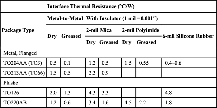
When screw-mounting a device that has to be isolated from the heat sink, you need to use an insulating bush either in the device tab or the heat sink. The preferred method is to put the bush in the heat sink, and use large flat washers to distribute the mounting force over the package. You can also use larger screws this way. The bush material should be of a type that will not flow or creep under compression; glass-filled nylon or polycarbonate is acceptable, but unfilled nylon should be avoided. The bush should be long enough to overlap between the transistor and the heat sink, to prevent flashover between the two exposed metal surfaces.
A fast, economical, and effective alternative is a mounting clip. When only a few watts are being dissipated, you can use board mounting or free-standing dissipators with an integral clip. A separate clip can be used for larger heat sinks and higher powers. The clip must be matched to the package and heat sink thickness to obtain the proper pressure. It can actually offer a lower thermal resistance than other methods for plastic packages, because it can be designed to bear directly down on the top of the plastic over the die, rather than concentrating the mounting pressure at the hole in the tab. It also removes the threat of flashover around the mounting hole, since no hole is needed in the insulating washer.
When you have to mount several identical flat (e.g., TO-220) packages to a single heat sink, a natural development of the clip is a single clamping bar that is placed across all the packages together (Fig. 9.17). The bar must be rigid enough and fixed at enough places with the correct torque to provide a constant and predictable clamping pressure for each package. With suitably ingenious mechanical design, it may also contribute to the total thermal performance of the whole assembly.
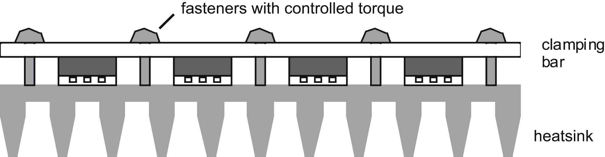
9.6.4. Placement and Layout
If you are only concerned with designing circuits that run at slow speeds with CMOS logic and draw no more than a few milliamps, then thermal layout considerations will not interest you. As soon as dissipation raises the temperature of your components more than a few tens of degrees above ambient, it pays to look at your equipment and PCB layout in terms of heat transfer. As was shown in Section 9.4.3, this will ultimately reflect in the reliability of the equipment.
Some practices that will improve thermal performance are as follows:
• Mount PCBs vertically rather than horizontally. This is standard in card cages and similar equipment practice, and it allows a much freer convective air flow over the components. If you are going to do this, do not then block off the air flow by putting solid metal screens above or below the boards; use punched, louvered, or mesh screens.
• Put hot components near the edge of the board, to encourage a good air flow around them and their heat sinks. If the board will be vertically mounted, put them at the top of the board.
• Keep hot components as far away as possible from sensitive devices such as precision op-amps or high failure rate parts such as electrolytic capacitors. Put them above such components if the board is vertical.
• Heat sinks perform best in low ambient temperatures. If you are using a heat sink within an enclosure without forced air cooling, remember to allow for the steady-state temperature rise inside the enclosure. However, do not position a heat sink near to the air inlet, as it will heat the air that is circulating through the rest of the enclosure; put it near the outlet. Do not obstruct the air flow over a heat sink.
• If you have a high heat density, for example a board full of high-speed logic devices, consider using a thermally conductive ladder fixed on the board and in contact with the IC packages, brought out to the edge of the board and bonded to an external heat sink. PCB laminates themselves have a low thermal conductivity.
• If you have to use a case with no ventilation, for environmental or safety reasons, remember that cooling of the internal components will be by three stages of convection rather than one: from the component to the inside air, from the inside air to the case, and from the case to the outside. Each of these will be inefficient, compared to conductive heat transfer obtained by mounting hot components directly onto the case. But if you take this latter course, check that the outside case temperature will not rise to dangerously high levels.
..................Content has been hidden....................
You can't read the all page of ebook, please click here login for view all page.