CHAPTER 8
![]()
Troubleshooting Discrete Circuits (Simple Transistor Amplifiers)
For this chapter we will be introducing transistor amplifiers that are “derived” from the LED circuits from Chapter 7. We shall be showing that these amplifiers have limitations such as amplitude gain (ratio of output signal to input signal amplitudes), waveform distortion (e.g., a sine wave input signal with a distorted waveform at the output), output swing, and output current. In general, an amplifier is a circuit that provides a larger voltage signal or larger current signal at the output when compared to the input signal. All amplifier circuits require some type of supply voltage such as a 9-volt battery or a 12-volt power supply.
Important Practical Transistor Specifications
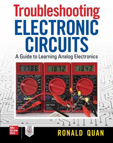
It should be noted that amplifiers are imperfect in that they cannot supply infinite current nor infinite voltage at their outputs. The transistors themselves have limitations on maximum collector-to-emitter voltage and maximum collector current, along with maximum power dissipation. For example, the ubiquitous 2N3904 NPN transistor has a typical maximum collector-to-emitter voltage (VCE) of 40 volts, a 200 mA maximum collector current (IC), and a 200 mW power dissipation rating. Power dissipation is usually given by Pd = VCE × IC. For example in Figure 8-1, suppose the collector current driving the light-emitting diode LED1 is 20 mA = IC, and we have 9 volts as the supply BT2 with a red LED1 with a 2-volt forward turn-on voltage = VF. BT2 = 9 volts and VF = 2 volts so BT2 = VF + VCE, and VCE = BT2 – VF or VCE = 9 volts – 2 volts, so:
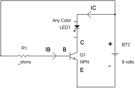
FIGURE 8.1 An LED drive circuit used for determining transistor Q1’s power dissipation.
VCE = 7 volts
Pd = VCE × IC, which is the power dissipation of transistor Q1
Pd = 7 volts × 20 mA
Pd = 140 mW, which is fortunately below the 200 mW power dissipation rating of the 2N3904
Although this example will work, as a rule of thumb, you want the power dissipation to be less than 50 percent of the maximum rating. In this example, the transistor is dissipating at 70 percent of maximum power dissipation (via 140 mW/200 mW = 70%), so we may want to use a higher wattage transistor, such as a 2N4401where Pd = 500 mW maximum.
Note that both VCE = 7 volts and IC = 20 mA are well within the maximum specifications of 40 volts and 200 mA, respectively, for the 2N3904 transistor. However, this example shows that we have to keep track of power dissipation even if the voltages and currents are well within specifications.
Simple Transistor Amplifier Circuits
The basic LED constant current source drive circuit shown in Figure 8-2 can be reconfigured to operate as an amplifier as shown in Figure 8-3.
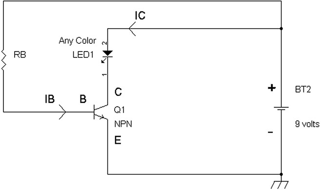
FIGURE 8.2 Constant current source to the LED via Q1’s collector current.

FIGURE 8.3 The constant current source LED drive circuit modified into an amplifier.
NOTE: The base driving resistor is renamed as RB.
In Figure 8-2 the transistor’s base-to-emitter voltage is held constant via the base current driving resistor RB that is connected to the power supply. With this constant base-to-emitter voltage, a constant collector current is provided to the LED. However, if we somehow are able to vary the base-to-emitter voltage by just a little, such as a variation of a few millivolts (mV), then the collector current will vary as well. See Figure 8-3, which is essentially the same circuit with a couple of modifications.
For this type of amplifier, the signals must be low level like the types of signals from microphones that produce < 10 mV to avoid distorted output signals. If larger signals are used such as an audio signal from your digital or CD player, then the input should be attenuated with a voltage divider circuit. Typical attenuation would lower the amplitude by 10 to 100 fold.
Although this circuit is “easy” to analyze, it has limited purposes on its own as an amplifier. However, some circuits do not require low distortion. This circuit can be used for a fuzz pedal distortion amplifier used in an electric guitar, or be used in an oscillator circuit, or be used as a mixer that deliberately generates distortion products, such as in an RF mixer.
First DC Analysis: Capacitors = Batteries with Self Adjusting Voltages
Capacitors C1 and C2 can be viewed as “fast charge” batteries that charge to a voltage such that no DC current flows through them. Let’s take a closer look at the one-transistor amplifier with some voltages labeled. See Figure 8-4 first.

FIGURE 8.4 Capacitors C1 and C2 are charged to voltages “VBE” and “VCE” as marked.
When we look at Figure 8-5, the DC voltage at Vin is equal to the series voltages of BT_C1 and the voltage at the base-emitter junction of Q1. Because the polarities of BT_C1 and VBE are the same with equal voltages via the + side of BT_C1 connected to the + side of VBE, the voltage at Vin is 0 volts DC. This amounts to two back-to-back equal voltage sources connected in series such that the net voltage is zero. Here is another way to look at this. Suppose you have a two-cell flashlight. Instead of installing the 1.5-volt batteries correctly (in series) to provide 3 volts, you install them back to back, which gives zero volts instead.

FIGURE 8.5 Batteries BT_C1 and BT_C2 can be thought of as replacing C1 and C2 as voltage sources.
In the amplifier, if the VBE of Q1 = 0.70 volts, capacitor C1 charges up to exactly 0.70 volts in Figure 8-4. In Figure 8-5, we see if BT_C1 is 0.70 volt as labeled, then the DC voltage at Vin has to be zero volts due to series connection of back-to-back VBE voltages from the Q1 and C1.
Likewise, if C2 in Figure 8-4 is charged up to a voltage of VCE, we see in Figure 8-5 that the DC voltage at Vout has to be zero volts. The reason is that BT_C2 has an equal and opposing voltage to VCE, the voltage at the collector of Q1. Thus, the DC voltage at Vout has to be zero volts due to the back-to-back series connection of VCE from the transistor and VCE in C2 or BT_C2.
The capacitors C1 and C2 play two important roles. First, they block out DC currents from Vin and Vout. Second, they pass through an AC signal such as an audio signal.
Second DC Analysis: Take Out the Capacitors to Find the DC Currents and DC Voltages
With the capacitors removed we can now more clearly see for DC analysis. Not only the capacitors C1 and C2 have been removed but the adjoining components R1 and R2 are now also no longer part of the circuit. What we are left with is just three components, RL, R2, and Q1, plus the power supply, BT2.
There are two reasons for determining the DC base and collector currents, IB and IC. Finding the expected base and collector currents will allow us to determine the collector-to-emitter voltage, which has to be > 0.7 volts in most cases. For example, if the collector current is too high or the voltage drop across RL is too high, then the transistor is in the saturation region, and the circuit will not amplify.
To determine the collector current IC, first, we calculate for the base current IB.
IB = (BT2 – VBE)/RB
For most good approximations, VBE = 0.7 volt.
IB = (BT2 – 0.7 v)/RB
![]()
Let’s take some examples pertaining to Figures 8-4 or 8-6:

FIGURE 8.6 To calculate the DC currents and voltages, remove all capacitors that are C1 and C2.
If BT2 = 9 volts and RB = 56kΩ, then IB = (9 v – 0.7 v)/56kΩ = (8.3 v)/56kΩ
IB = 0.148 mA or IB = 148 μA
IC = β IB
For this example, we use a lower current gain transistor such as a 2N3903 where β = 50. Since we already calculated the base current as IB = 0.148 mA then:
IC = β IB = 50 × 0.148 mA
IC = 7.4 mA
If we have RL = 1000Ω, then we can now find VC, Q1’s collector voltage reference to ground.
VC = BT2 – IC (RL)
VC = 9 v – 7.4 mA (1000Ω) = 9 v – 7.4 v
VC = 1.6 volts
What happens if β → 100?
Then IC = β IB = 100 × 0.148 mA = 14.8 mA.
We find that VC = 9 v – 14.8 mA (1000Ω) = 9 v – 14.8 v = –5.8 volts = VC???.
This is not possible since we only have a positive power supply and thus no negative volts can be generated. Instead, VC ~ 0 volts, and usually VC ~ 0.2 volt. That is, if the calculated value for VC is < 0.5 volt, usually the amplifier will not work because the transistor is now a switch that “shorts” the collector terminal to ground.
What we have shown in this example is that if the current gain is too high, the transistor amplifier in Figure 8-4 can cause the transistor to turn into a switch. That is why a circuit like Figure 8-4 requires selecting the β of transistors in a narrow range, such as 30 < β < 50, or “tweaking” the resistance value of the base driving resistor, RB.
For example, if we want to use a transistor whose β = 100, then we should approximately double the value of RB from 56kΩ to 110kΩ with BT2 = 9 v and RL = 1000Ω. This leads to:
IB = (BT2 – 0.7 v)/RB = (9 v – 0.7 v)/110kΩ = 8.3 v/110kΩ = 75.455 μA
IC = 100 × 75.455 μA = 7.545 mA
VC = BT2 – IC RL = 9 v – 7.545 mA × 1000Ω = 9 v – 7.545 v = VC
VC ~ 1.45 volts, which is pretty close to VC = 1.6 volts for RB = 56kΩ and β = 50.
It would be safer to aim for a slightly higher VC. We can have RB = 120kΩ with β = 100 and RL = 1000Ω, which results in IB = 69.167 μA and IC = 100 × 69.167 μA or IC = 6.9167 mA.
VC = 9 v – 6.9167 mA × 1000Ω = 9 v – 6.9167 v = VC
VC = 2.08 v
In the real world, the specific transistor part number (e.g., 2N3904, 2N2222, etc.) will not only have a range of β, but the current gain β will change with temperature. So, the DC collector current and DC collector voltage will vary. In general, the transistor amplifier in Figure 8-4 is more of a hobbyist or DIY (do-it-yourself) amplifier where you have to individually tweak it to a desired collector current. We will find in the next section that the DC collector current IC also determines the AC signal’s gain at Vout, and also the input loading resistance at Vin.
For now, we have:
VC = BT2 – IC (RL)
![]()
A more general formula would be:

Alternatively, instead of using the general formula for VC, sometimes it’s more logical to find the base current, IB, first and then calculate the collector current, IC to find VC, the collector voltage.
If BT2 = 5 volts and RB = 100kΩ, then IB = (5 v – 0.7 v)/100kΩ = (4.3 v)/100kΩ.
IB = 0.043 mA or IB = 43 μA
If β = 78, then IC = β IB = 78 (43 μA).
IC = 3.225 mA
Let RL = 820Ω
VC = BT2 – IC (RL) = 5 volts – 3.225 mA (820Ω) = 5 volts – 2.6445 volts = VC
VC = 2.3555 volts
Finding the AC Signal Gain
The DC collector current is the most important DC characteristic to find for calculating the AC signal gain. Via the DC collector current we can also calculate the input resistance.
Input resistance to an amplifier is important since the input signal source itself usually has an output source resistance or an optimum input load resistance. For example, an antenna may have a 50Ω source resistance. To achieve maximum power transfer, the input resistance of the amplifier should be 50Ω as well.
In another example, if your signal source is a dynamic microphone, then the input resistance should be typically 1000Ω or more. If you should connect the dynamic microphone to an amplifier with a 50Ω input resistance, then you will lose signal amplitude from the microphone.
Thus, we have to keep in mind the amplifier’s input resistance based on the application (e.g., RF amplifier, microphone preamplifier, sensor amplifier, etc.). This is particularly important when we have one amplifier’s output connected to the input of a second amplifier.
We can find the AC signal gain of this amplifier by noting the following:
• Capacitors with “sufficiently large” capacitances to be like batteries are AC short circuits or zero ohm resistors for AC signals.
• Power supplies are also treated as AC short circuits or zero ohm (0Ω) resistors with respect to AC signals.
At first glance, the second item may seem absurd. But it you think about it, if you probe for AC signals in a clean power supply or battery, you will find no AC signal. By definition, power supplies and batteries are DC voltage sources and thus cannot include any AC signal.
Likewise, if a capacitor has a large enough capacitance that it acts like a “battery” (e.g., see Figure 8-5 again), then again by definition a battery cannot include an AC signal; it only produces a DC voltage. Let’s take a look again at the “original” schematic in Figure 8-7.

FIGURE 8.7 The one-transistor amplifier from Figure 8-5.
Now let’s take a look at the AC analysis model shown in Figure 8-8.
FIGURE 8.8 The capacitors C1, C2, and battery (DC power supply) BT2 are “modeled” as AC short circuits or AC zero ohm wires.
Figure 8-8 can be further redrawn to look simpler or more intuitively familiar. See Figure 8-9.
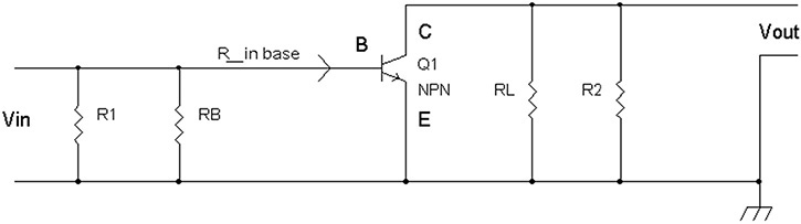
FIGURE 8.9 A redrawn version of Figure 8-8 to show a more intuitive idea of the one-transistor amplifier’s AC analysis circuit.
As you can see in Figure 8-9, the circuit looks a little “funny” in that there is no power supply. However, the schematic gives us an idea of how the AC signal at Vin will be amplified. Note that there is a resistance into Q1’s base, which is referenced to ground.
Finally, we can model Figure 8-9 in terms of a block diagram with the resistors R1, RB, RL, and R2. See Figure 8-10. Note that R_in base is now “modeled” as a resistor to ground along with R1 and RB.
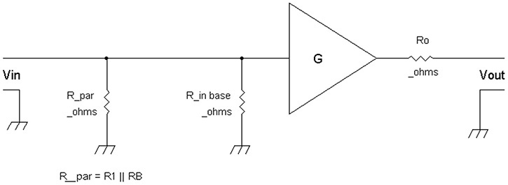
FIGURE 8.10 A block diagram of Figure 8-9’s AC analysis circuit.
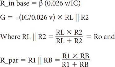
In order to complete the AC analysis circuit, we have to find two “unknowns,” resistor, R_in base, and the gain, “G.” See below for the formulas given that IC = DC collector current.
Sometimes it is convenient to express the term (0.026 v/IC) = re, where a handy starting point of IC = 1 mA results in:
(0.026 v/0.001A) = 26Ω = re
From this 1 mA starting point we can find re for any other collector by a scaling factor such that re is inversely proportional to collector current. That is, for a given current:
![]()
Since we often set collector currents in milliamps, mA, you can express the formula this way where the collector current IC is in milliamps.
![]()
![]()
And if IC = 0.1 mA = 100 μA, then ![]()
For the input resistance R_in base:
R_in base = β (0.026 v/IC) = β re
NOTE: R_in base is inversely proportional to IC. For example, if you decrease IC by tenfold, then R_in base increases by tenfold.
For example, if β =100 and IC = 1 mA, then ![]()
re = 26 Ω
R_in base = β re = 100 × 26Ω = 2.6KΩ
If β =100 and we have IC = 0.1 mA, then R_in base = β re = 26KΩ.
For the gain factor G:
G = –(IC/0.026 v) × RL || R2
NOTE: G is proportional to the DC collector current IC. So, if you increase IC by tenfold (e.g., 0.1 mA to 1 mA), the gain, G, goes up by tenfold. And if you decrease IC by tenfold, G, decreases by tenfold.
In this amplifier given current gain β, if you increase the DC collector current the input resistance to the base, R_in base, decreases while the gain, G, increases.
A decreasing R_in base can cause the input signal to be loaded down and thus attenuated when we increase the DC collector current IC. One way to offset this is to pick a transistor that has a higher β. For example, a 2N3904 may have a typical β of 150, but a 2N5088 has higher typical β of 300. So, if you want to increase the collector current twofold but keep the same R_in base resistance, you can select a transistor with twice the β. To keep the same DC collector current IC, this also means that RB would be increased about twofold in resistance because of the higher current gain (e.g., twice the β).
Now let’s take one of the previous examples concerning DC analysis:
BT2 = 5 volts, RB = 100kΩ, then IB = (5 v – 0.7 v)/100kΩ = (4.3 v)/100kΩ
IB = 0.043 mA or IB = 43 μA
If β = 78, then IC = β IB = 78 (43 μA) = 3.225 mA.
IC = 3.225 mA = 0.003225A
RL = 820Ω
R1 = R2 = 220 KΩ
Let C1 = C2 = 33 μf (with C1and C2 rated at ≥ 16 volts), RL = 820Ω, R2 = 100KΩ, with IC = 0.003225 A.
Gain Calculation
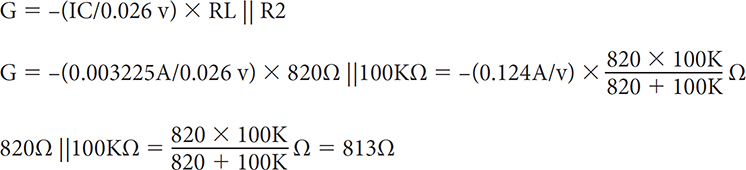
NOTE: The units A/v or amps per volt has a unit of (1/resistance) or 1/Ω.
The minus sign indicates an inverted AC signal, or a signal that is 180 degrees out of phase.
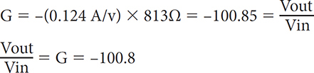
For example, if Vin is a 1 mV peak sinewave, then Vout provides an inverted sinewave at 100.8 mV peak.
Base Resistance, R_in Base Calculation
R_in base = β (0.026 v/IC) = 78 (0.026 v/0.003225A) = 78 (8.06Ω)
NOTE that the units v/A or volts per amp has a unit of resistance or Ω.
R_in base = 628.8Ω
Limitations of This One-Transistor Amplifier
We will now look at the one transistor amplifier in terms of input amplitude range. See Figure 8-11.
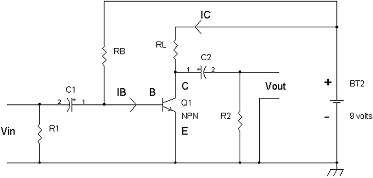
FIGURE 8.11 The one-transistor amplifier that requires a low-level input signal to avoid distortion.
Limited Input Amplitude Range
When Vin is driven with a low-impedance generator such as one that has a 50Ω source resistance, which is common in many function generators, this amplifier will start to distort with signals starting at about 1-mV peak sine wave. For example, a 10-mV peak signal that is 20 mV peak to peak at the input will result in Vout having a generally larger amplitude but also a waveform that is distorted with about 10 percent second order harmonic distortion. As an example, if the frequency is 1000Hz, the output signal will provide a signal at 1000Hz, and another one at 2000Hz at 10 percent of the amplitude at 1000Hz.
Because this amplifier can produce so much distortion with signal sources from portable music players or smartphones (> 100 mV peak), you would need to place a voltage divider circuit such as a volume control to adjust the level into Vin, the input terminal.
See Figure 8-12 for an amplifier with the following:
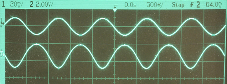
FIGURE 8.12 Amplifier 20 mV peak to peak signal input on top trace. Bottom trace shows a 2.7-volt peak to peak (inverted) output signal with 10 percent second harmonic distortion; and notice the rounder positive cycle and narrower negative cycle.
R1 = 10MegΩ, R2 = 10MegΩ, RB = 4.7MegΩ, RL = 12KΩ, IC = 0.3375 mA IC = 0.0003375 A, or IC = 337.5 µA
Q1 = 2N3904, BT = 9 volts
G ~ –145 as measured with 20 mV peak to peak sinewave at Vin with a 50Ω source resistance generator.
G = –144 as calculated. That is, G = –(0.0003375A/0.026 v) 12KΩ ~ –144.
NOTE: 12KΩ || 10MegΩ = 12KΩ within about 0.12%.
See below for the input and output signals.
We can mitigate the distortion problem by using a series resistor, R_ser, as shown in Figure 8-13.
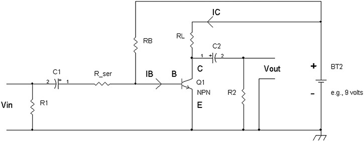
FIGURE 8.13 Lower distortion for the same output swing.
Typically, if we want lower distortion from an amplifier, we have to give up some of the voltage gain.
For example, if the gain of the amplifier is about 145, we can have lower distortion for the same output voltage if we set the series base resistor at about 10 × R_in base. Again, if we use the previous example with:
R1 = 10MegΩ, R2 = 10MegΩ, RB = 4.7MegΩ, RL = 12KΩ, IC = 0.3375 mA or IC = 337.5 μA
Q1 = 2N3904, BT = 9 volts
IB is then calculated as about (9 v – 0.7 v) 4.7MegΩ = 1.766 μA. We can now find β = IC/IB = (337.5 μA/1.766 μA):
β = 191
This leads to R_in base = β(0.026 v/IC) or R_in base = 191(77Ω).
R_in base = 14.7KΩ. If we make R_ser about 10x of R_in base, then R_ser ~ 150KΩ. The resulting distortion can now be compared with R_ser = 0 Ω and R_ser = 150KΩ for gain and distortion at Vout for the same output voltage. See Table 8-1 that shows the effect on distortion with different values for input series resistor, R_ser. There is a trade-off in that you can have lower distortion but at the expense of lower voltage gain.
TABLE 8.1 Distortion Measurements for the Same Amplitude Output at Vout
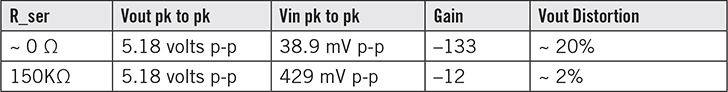
NOTE that with the gain reduced by about tenfold, the distortion is reduced by ~10 as well. Also it is preferred that RB >> R_ser for reducing distortion.
See Figures 8-14 and 8-15, where the top trace waveforms are the input signals, and the bottom traces show the output signals. Note the phase inversions between output and input signals.
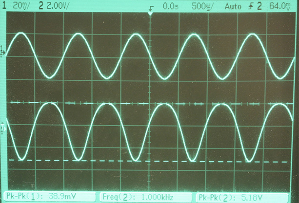
FIGURE 8.14 Output waveform on the bottom trace with R_ser = ~ 0 Ω, and note the compression on the positive cycle and narrowing on the negative cycle that denotes 20 percent harmonic distortion.
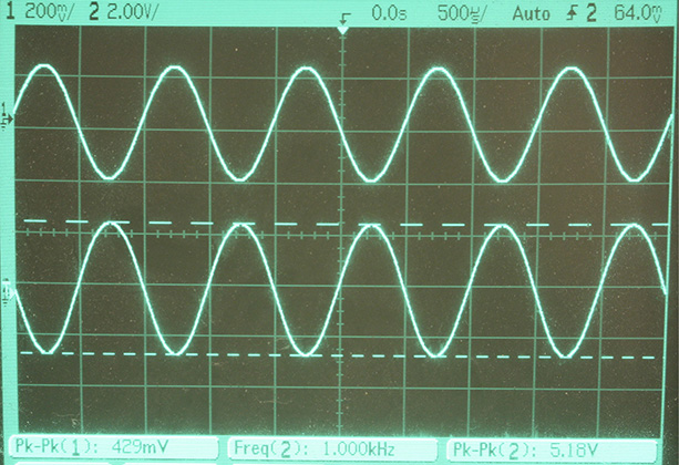
FIGURE 8.15 Output waveform on bottom trace with R_ser = 150KΩ, which shows almost no compression or narrowing distortion compared to Figure 8-14. Harmonic distortion was measured at approximately 2 percent.
Figure 8-15 shows when a “linearizing” series 150K resistor is added.
Output Swing Determined by IC and RL || R2
To maximize output voltage swing, we should bias the collector current, IC, such that the DC collector voltage is in a range of 40 to 60 percent of the supply voltage. For example, if the supply voltage such as BT2 in Figure 8-13 is 10 volts (e.g., 8 AA rechargeable 1.25-volt batteries in series), then a good starting point will be at the 50 percent of 10 volts or 5 volts DC at the collector of Q1. RB would be selected for this. The reason we want the DC collector voltage close to 50 percent of the supply voltage is to provide maximum output AC voltage swing. However, depending on the application, sometimes we just need a few volts of AC swing, peak to peak.
The maximum peak voltage swing without distortion is calculated as:
Vout max peak to peak = 2 × IC × RL||R5, where VC ≥ 50% of power supply voltage
For example, suppose you have BT2 = 6 volts and RL = 3KΩ, and you bias RB such that:
IC = 1 mA DC
This means that VC = 6 volts – IC(RL) = 6 volts – 1 mA (3KΩ) = 6 volts – 3 volts or VC = 3 volts.
VC = 3 volts, which is 50 percent of BT2 = 6 volts. This is a good starting point. If R5 is >> RL, such as RL = 1MegΩ, then the output AC voltage swing will be close to 6 volts peak to peak.
This is because with R5 >> RL, RL || R5 ~ RL:
Vout max peak to peak = 2 × IC × RL||R5 ~ 2 × IC × RL = 2 × 1 mA × 3KΩ = 2 × 3 volts
Vout max peak to peak ~ 6 volts peak to peak
However, if R5 = RL, then RL || R5 = 0.5 RL and the voltage swing will be reduced by 50 percent. For example, when RL = 3KΩ and R5 = 3KΩ, the output voltage swing is reduced by 50 percent.
Vout max peak to peak = 2 × IC × RL||R5 = 2 × IC × RL||RL = 2 × IC × 0.5 RL = IC × RL = Vout max peak to peak
Vout max peak to peak = 1 mA × 3KΩ = 3 volts peak to peak
If the 3 volts peak to peak Vout max is sufficient, then you do not need to change the circuit. However, if R5 is lower in value such as 2KΩ or 1KΩ and you still want 3 volts peak to peak output, then you have to make RL a smaller resistance such as lowering it to 2KΩ or 1KΩ while reselecting RB to have VC = 3 volts DC such that the DC collector current, IC is increased.
So far, the one-transistor amplifier circuits presented have many variables in terms of gain, input resistance, and DC operating points such as collector current IC and collector voltage VC due to the variation in β, the current gain. If you need to build many of these amplifiers and make them repeatable, you can buy the transistors in tape form as shown in Figure 8-16. They should be reasonably matched in terms of turn-on voltage and β, but check them with a DVM for confirmation.
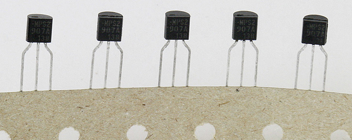
FIGURE 8.16 Transistors on tape are reasonably matched for β and VBE turn-on voltage.
Troubleshooting the One-Transistor Amplifier
The one-transistor amplifier may not work for the following reasons:
• If the transistor is put in backwards with the collector and emitter swapped, then the collector current will be very low because β → 1 or 2. This will result in very low gain since the collector current will be too small. So, expect VC to be almost the same voltage as the power supply, which says that the voltage across RL is close to zero volts.
• If the collector and emitter terminals are reversed, and the power supply voltage is > 6 volts DC, there’s a good chance that the transistor will act like a Zener diode, and the voltage at the collector will be in the range of 5 or 7 volts DC, but there will be very little signal output at Vout.
• If you replace the transistor, but find that the output signal is low, check the DC collector voltage, VC. If the collector’s voltage VC is close to 0 volts (e.g., < 0.5 volt), the transistor is in saturation because there is too much base current. Reselect the base driving resistor, RB, to have VC at about half the supply voltage, or select a transistor with lower current gain, β. You may also have to confirm the proper resistance values for RL and RB. If RL is too high in resistance and or if RB is too low in resistance, it can cause the transistor to be in saturation.
• If you think you connected everything correctly but you find strange DC readings and output signals, make sure the transistor is the correct polarity (e.g., NPN or PNP). Sometimes it’s easy to inadvertently put in the wrong polarity transistor and/or put it in with swapped leads.
• Check power supply voltage, and always add a bypass capacitor such as 0.1 μf to 1 μf across the power supply voltage source close to the transistor amplifier. Also note the supply voltage and choose the bypass capacitor to have at least twice the voltage rating. For example, if the supply voltage is 12 volts, choose a 25-volt to 100-volt capacitor.
Using Negative Feedback to Build “Mass Production” Amplifiers
If we look at the one-transistor amplifier schematic in Figure 8-13 with its output waveform in Figure 8-14, we will notice that the AC signal going into the base produces a signal at the collector that is in negative phase or opposite phase of the input.
This makes sense because the DC collector voltage, VC = BT2 – IC (RL). Since IC is proportional to base current, IB, and IB is some function of the base voltage, then an increase in base current causes an increase in collector current. But an increase in collector current, IC, causes a decrease in VC due to VC = BT2 – IC (RL). For example, if BT2 = 10 volts, RL = 1KΩ, then VC = 5 volts – IC 1KΩ. If we start out with IC = 1 mA, then VC = 5 volts – 1 mA 1KΩ = 5 volts – 1 volt.
VC = 4 volts
Suppose we increase the collector current such that IC → 3 mA, then:
VC = 5 volts – 3 mA 1KΩ = 5 volts – 3 volts = 2 volts
VC = 2 volts
As we can see, an increase in collector current results in a decrease in collector voltage. Since an increase in base current causes an increase in base voltage, then it follows that an increase in base voltage causes an increase in collector current, which causes a decrease in collector voltage. Thus, we have a “negative” phase relationship between the base and collector terminals. If we have this relationship, we can apply a self-biasing resistor between the base and collector as shown in Figure 8-17. If this resistor is chosen properly, we can set a DC collector voltage and collector current that is not as sensitive to β variations. As long as β >> 1 such as β ≥ 20, the DC collector current that is set by this circuit will not vary much whether the transistor has a β of 50 or a β of 500. Also, as long as the AC signal’s gain is kept to ≤ 10, the gain will be set by two resistors and it again will be insensitive to β variations.
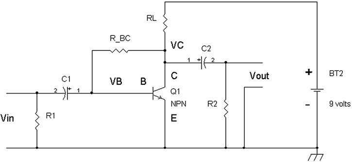
FIGURE 8.17 A simple self-biasing one-transistor amplifier via R_BC for “insensitivity” to β.
DC Analysis of Self-Biasing Amplifier
With a negative feedback resistor R_BC that is connected from the collector to base, a DC voltage is established at VC. For the DC analysis, see Figure 8-18.
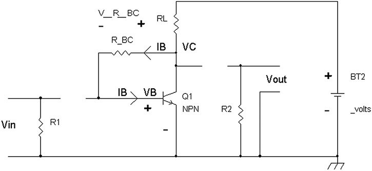
FIGURE 8.18 DC analysis circuit for the self-biasing one-transistor amplifier via removing the DC blocking capacitors.
Typically, the base-emitter voltage at VB is ~ 0.7 volt. If Q1’s β is greater than 50, then there’s a good chance that Q1’s base current, IB, is very small such that there is a very small voltage across R_BC, V_R_BC = IB × R_BC. (Refer to Figure 8-18.)
NOTE that VC = V_R_BC + VB or VC = (IB x R_BC) + VB.
If this voltage across resistor R_BC, V_R_BC << 0.7 volt, then VC ~ VB. A commonly used transistor, such as2N4124 or equivalent, generally has β ≤ 50 at currents from 100 μA to about 20 mA.
For power supply voltages that are >> 0.7 volts (e.g., ≥ 5 volts) even with base current IB flowing through R_BC in the order of V_R_BC = 0.7 volts such that VC = 1.4 volts versus VC = 0.7 volts, the collector current will vary < 25 percent for BT2 ≥ 5 volts.
For example, with BT2 = 5 volts, IC ~ (BT2 – VC)/RL.
With VC = 0.7 volt, IC ~ (5 volts – 0.7 volt)/RL or IC0.7v ~ 4.3 volts/RL.
With VC = 1.4 volts, IC ~ (5 volts – 1.4 volts)/RL or IC1.4v ~ 3.6 volts/RL.
We can take the ratio of the two collector currents for VC = 0.7 volt and 1.4 volts to determine the change in collector current.
(IC0.7v/IC1.4v) = [(4.3 volts/RL)/(3.6 volts/RL)], the RL’s cancel out, leaving (IC0.7v/IC1.4v) = (4.3 volts/ 3.6 volts) = 1.1944, which is a 19.44 percent change in collector current.
Let’s take a look at some typical component values. Q1 = 2N4124 or 2N3904, BT2 = 5 volts, RL = 3300Ω, R_BC = 100KΩ, with β = 170, the measured VC = 1.3 volts. The collector current with β = 170 is:
IC ~ (5 volts – 1.3 volts)/3300Ω = 1.12 mA = IC
If we replace Q1 with a 2N5089 where β = 461, VC = 0.9 volt, and IC = (5 volts – 0.9 volts)/3300Ω = 1.24 mA for β = 461, which is only about a 10.8 percent change with 1.12 mA for β = 171. So even when β increased from 170 to 461, a 2.77-fold increase, the collector current, IC, only increased by about 10.8 percent.
Having VC biased at a DC voltage of about 1 volt will limit the voltage swing from about 0 volt to about 2 volts or 2 volts peak to peak before clipping of the output waveform occurs.
To maximize output voltage swing, it is generally better to have VC set to about one half the supply voltage. For example, if BT2 = 5 volts, and VC is set to 2.5 volts DC, then the output swing can be from about 0 volts to nearly 5 volts, or close to 5 volts peak to peak. By adding a resistor (R_BE) across the base-emitter terminals, we can raise VC’s DC voltage. See Figure 8-19.
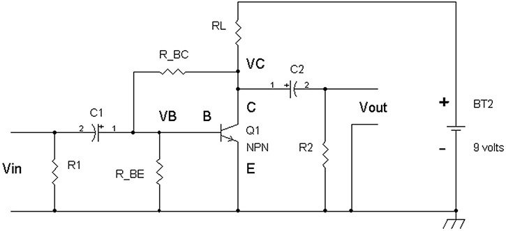
FIGURE 8.19 Adding an extra resistor R_BE to form a voltage divider with R_BC.
By adding R_BE, we can raise the DC collector voltage. See Figure 8-20 for the DC analysis schematic.
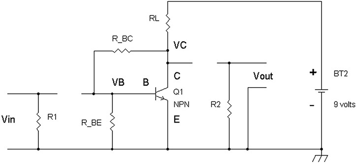
FIGURE 8.20 DC analysis circuit for Figure 8-19.
Since VB ~ 0.7 volt, we can work backwards to find VC since the voltage across R_BE is ~ 0.7 volt. By using a voltage divider formula and neglecting the base current from Q1, we have:
0.7 volt = VB = VC [R_BE/(R_BE + R_BC)]
0.7 volt/[R_BE/(R_BE + R_BC) ] = VC
VC = 0.7 volt [(R_BE + R_BC)/R_BE]
In essence the DC voltage at the collector, VC, is a scaled “up” voltage of VBE.
For example, if we want VC = 1.4 volts, then R_BC = R_BE.
VC = 0.7 volt [(R_BE + R_BE)/R_BE ] = 0.7 volt [2R_BE/R_BE ] = 0.7 volt × 2
VC = 1.4 volts
A general formula where it is easier to just find the ratio of R_BC to R_BE based on having a specified VC is shown here:
R_BC/R_BE = (VC/0.7 v) – 1
For example, if BT2 = 5 volts, RL = 3300Ω, and we want VC = 2.5 volts, then:
R_BC/R_BE = (2.5/0.7 v) – 1 = 3.57 – 1 = 2.57
R_BC = 2.57 (R_BE)
We can make R_BE = 39KΩ so that R_BC = 2.57 (39KΩ)
R_BC = 100KΩ
In general VC will be a bit higher than calculated using a general-purpose transistor such as with a 2N4124 transistor. With a higher β transistor such as a 2N5089, the calculated VC voltage will be closer in practice.
To preserve good voltage swing, R_BC >> RL. For example, if RL = 1KΩ, R_BC ≥ 10KΩ. However, we will see that the simple 1 transistor amplifier has a “drawback” in terms of input resistance being too low. But not to worry—we use the lower input resistance to our advantage by adding a series input resistor to set the gain of the amplifier (see R1" in Figure 8-25 if you are curious)..
AC Analysis of a Self-Biased Amplifier
Adding the feedback resistor R_BC causes a lower total input resistance as “seen” by Vin (see Figure 8-21).
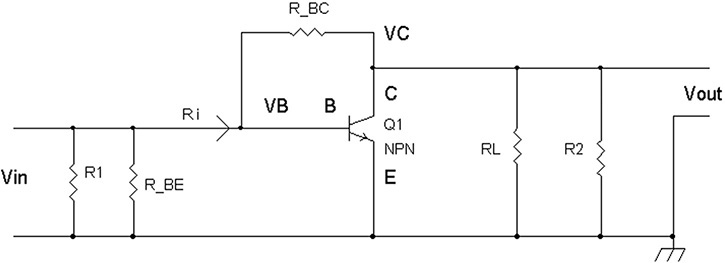
FIGURE 8.21 AC analysis circuit for the one-transistor feedback amplifier.
With negative feedback via the collector to base resistor, R_BC, this resistor and with the amplifier’s gain, G, will result in a low-value resistor, Ri, referenced to ground, where Ri is in parallel with R1 and R_BE.
Ri ~ [R_BC/(1 – G)] || R_in base, where G = Vout/Vin, and since this is an inverting amplifier, G will be a negative number.
G ~ –(IC/0.026 v) × (RL || R2 || R_BC)
The gain, G, is calculated to be the same as the simple transistor amplifier shown in Figure 8-10 when R_BC >> RL || R2. For a good enough approximation where R_BC ≥ 10 × (RL || R2), use:
G ~ –(IC/0.026 v) × (RL || R2)
For example, if the supply voltage BT2 = 12 volts, Q1 = 2N5089 where β = 400, RL = 4700Ω, R_BC = 100KΩ, R_BE = 20KΩ and VB = 0.7 volt, then VC = 0.7 v [(R_BC/R_BE) + 1].
VC = 0.7 volt [(100K/20K) + 1] = 0.7 volt [6]
VC = 4.2 volts
IC ~ (BT2 – VC)/RL = (12 volts – 4.2 volts)/4700Ω = 7.8 volts/4700Ω
IC ~ 1.66 mA = 0.00166 A
Let R2 = 1MegΩ so that RL || R2 = 4700Ω || 1MegΩ ~ 4700Ω = RL || R2.
G ~ –(IC/0.026 v) × (RL || R2)
G ~ –(0.00166 A/0.026 v) × (4700Ω)
G ~ –300
R_in base = β(0.026 v/IC) = 400(0.026 v/0.00166 A)
R_in base = 6.26KΩ = internal resistance across the base and emitter of Q1
Ri ~ [R_BC/(1 – G)] || R_in base
Ri ~ [100KΩ/(1 – –300)] || 6.26KΩ = [100KΩ/(1 + 300)] || 6.26KΩ Ri ~ 332Ω || 6.26KΩ
Since 332Ω << 6.26K, 332Ω || 6.26KΩ ~ 332Ω, which leads to an approximation of:
Ri ~ 332Ω
R_in base is the resistance into the base-emitter junction of the transistor that does not include any of the other external resistors such as R_BC, R_BE, and R1.
The resistance [R_BC/(1 – G)] is due entirely to Vin’s signal current flowing through R_BC, which results in a lower equivalent resistor, R_BC/(1 – G) referenced to ground. So, the question arises as to how we get such a lower equivalent resistor that is related to the amplifier’s gain, G? See Figure 8-22.
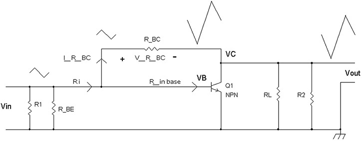
FIGURE 8.22 Input and output waveforms showing increased AC voltage across R_BC.
The amplifier produces an amplified (e.g., a larger amplitude) signal at the output, Vout, which is in opposite phase of the smaller amplitude input signal, Vin. This opposite phase signal at Vout then pulls extra current through the resistor R_BC. By pulling extra current, it makes it appear that Vin is driving an equivalently lower-value resistor that is referenced to ground like R1.
An example of this lowered resistance effect is if we imagine that the gain, G = –1 and R_BC = 1KΩ, then what happens when Vin = +1 volt? The output voltage is then – 1volt due to G = –1. However, the current flowing through the 1KΩ has a potential difference of +1 v – –1v or 2 volts. This means the resistor current is now 2 v/1KΩ = 2 mA. A +1-volt input across an equivalent resistor referenced to ground that will drain 2 mA would result in a 500Ω resistor since 1 v/500Ω = 2 mA.
In general, the voltage across resistor R_BC is V_R_BC, which has Vin on one side and Vout on the other side. Thus, V_R_BC = Vin – Vout, but Vout = –G Vin, so:
V_R_BC = Vin – –GVin = Vin + G Vin
V_R_BC = Vin (1 + G)
The current through R_BC is then:
I_R_BC = V_R_BC/R_BC
and by substituting Vin (1 + G) for V_R_BC:
I_R_BC = Vin (1 + G)/R_BC
We want to now model an equivalent resistor referenced to ground (as shown in Figure 8-23) that will drain the same amount of current as I_R_BC, which is I_R_BC = I_equiv = Vin(1 + G)/R_BC.
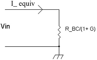
FIGURE 8.23 Equivalent resistor referenced to ground that drains the same current as I_R_BC.
Let’s see if the current, I_equiv, is the same as I_R_BC.
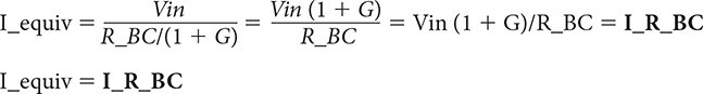
This confirms that the equivalent resistor referenced to ground is R_BC/(1 + G).
This makes sense because it would take a smaller-value resistor referenced to ground with just Vin applied to it to drain the same amount of (higher) current that would have to be a resistor divided in value by (1 + G). See Figure 8-24.
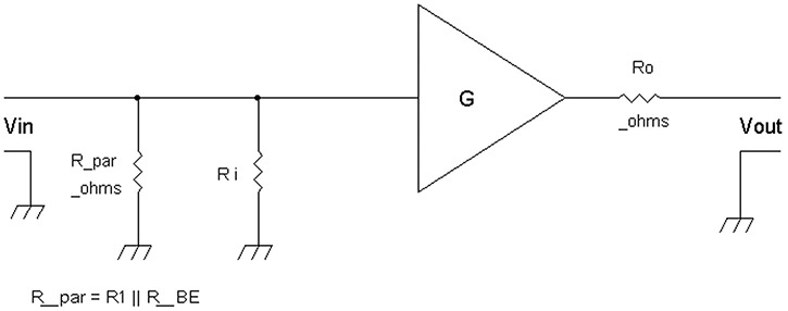
FIGURE 8.24 AC model where Ri = [R_BC/(1 – G)] || [R_in base].
Note if the amplifier has no gain where G = 0 that causes Vout = 0 volt, then essentially R_BC is shorted to ground on the collector of Q1, and we do indeed have R_BC as the equivalent resistor reference to ground.
R_BC/(1 + G)
with G = 0
R_BC/(1 + 0) = R_BC
The output resistance, Ro, is actually dependent on the input signal’s series source resistance. If Vin is driven by a pure voltage source or very low output impedance amplifier, Ro = RL||R2||R_BC, which is similar to the simple amplifier in Figures 8-3 and 8-7. Normally, R_BC >> RL||R2, so Ro ~ RL||R2.
Because R_BC lowers the overall input resistance seen by Vin to almost “short” circuit compared to the other resistors, R1, R_BE, and R_in base, generally, we do not drive the input directly with a signal source with low source resistance.
However, we can improve upon the amplifier in Figure 8-19 by adding a series resistor that will lower the gain, Vout/Vin, but then improves on raising the input resistance, lowering the output resistance, and also lowering the distortion for the same amplitude output. See Figure 8-25.
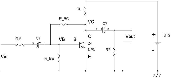
FIGURE 8.25 A modified one-transistor feedback amplifier with a series input resistor, R1".
We can define the gain ![]() that is relative to the signal voltage at the base of Q1, VB and Vout, and not taking R2 into account for now.
that is relative to the signal voltage at the base of Q1, VB and Vout, and not taking R2 into account for now.
And then we can define the actual gain ![]() .
.
Output Resistance Ro'
The reader can skip over this section pertaining to the output resistance, Ro', if desired. These calculations are long. The gist is having R_BC as a feedback resistor results in a lower output resistance than RL||R2.
The output resistance, Ro', not including R2 is approximately:
Ro' = {[(R_BC + R_in base || R_BE || R1")/(R_in base || R_BE || R1")] × (0.026 v/IC)} || RL
Here are a couple of calculations with their measured results.
With BT2 = 5 volts, RL = 2700Ω, R_BC = 100KΩ, R_BE = 40.2KΩ, and R1" = 20KΩ, the calculated gain (Vout/Vin) = –(R_BC/R1") = –100K/20K.
Vout/Vin = –5.0
Measured gain is –4.5, within 10 percent of the expected gain of –5.
Now let’s calculate the output resistance, with R2 removed from the circuit in Figure 8-25.
The calculated VC ~ VBE (1 + R_BC/R_BE) where VBE ~ 0.7 v:
VC ~ 0.7 v(1 + 100K/40K) = 0.7 volt (3.5)
VC ~ 2.45 volts. The measured VC was 2.3 volts.
With BT2 = 5 volts and VC = 2.45 volts with RL = 2.7KΩ, the calculated IC ~ (BT2 – VC)/RL since R_BC = 100KΩ >> RL = 2.7KΩ:
IC ~ (5 v – 2.45 v)/2.7KΩ
IC ~ 0.907 mA
The current gain β ~ 450 for the 2N5089.
R_in base = β (0.026 v/0.000907A) = 450(286Ω)
R_in base = 12.9KΩ
With R_BC = 100KΩ, R_in base = 12.9KΩ, R_BE = 40.2KΩ, R1" = 20KΩ, and RL = 2700Ω
Ro' ~ {[(R_BC + R_in base || R_BE || R1") /(R_in base || R_BE || R1")] × (0.026 v/IC)} || RL
where R_BC in parallel with RL is neglected since R_BC = 100KΩ >> RL = 2.7KΩ.
Therefore: Ro'~ {[(100KΩ + (12.9KΩ|| 40.2KΩ||20KΩ)/ (12.9KΩ||40.2KΩ||20KΩ)] × (0.026 v/0.000907 A)}|| 2.7KΩ
NOTE: (12.9KΩ||40.2KΩ||20KΩ) = 6.56KΩ.

Ro' ~ 390Ω measured via setting R2 = 390Ω and noticing that the signal dropped by 50 percent.
The output resistance, Ro', calculation is rather long, and sometimes we do not have time to do this. Here are some rules of thumb concerning the transistor amplifier.
1. Use low-value gains that are typically less than 5 or 10, such that R_BC/R1" ≤ 10.
2. Make sure that R_BC >> RL by at least tenfold. Thus, R_BC does not lower the gain G by much since as “seen” by the collector of Q1, RL and R_BC are essentially in parallel. The reason is that the resistors R_BE and R_in base that are coupled to ground and connected to R_BC at the base are << R_BC, that is (R_BE || R_in base) << R_BC.
3. Bias the DC voltage at the collector, VC, to be at one-half the power supply voltage.
4. Use as high β transistor as you can, such as a 2N5089. If you use a lower β transistor such as a general-purpose type, 2N3904, then you may have to set for lower gains such as R_BC/R1" ≤ 5.
5. Generally, bias the collector current, IC, in the range of 0.2 mA to 5 mA with the appropriate value RL resistor that is scaled from the example at ~ 1 mA where RL = 2700Ω. For instance, if you are running IC at 200 μA, then RL ~ 5 × 2700Ω or about 12KΩ, and R_BC ~ 5 × 100KΩ = 510KΩ, R_BE ~ 5 × 40.2KΩ = 200KΩ, and R1" = 100KΩ. Going the other direction with IC = 5 mA, all the resistors that were used for IC ~ 1 mA are scaled by (1/5) or 20 percent or 0.2. Thus, RL ~ 0.2 × 2700Ω ~ 560Ω, R_BC ~ 0.2 × 100KΩ ~ 20KΩ, R_BE ~ 0.2 × 40.2KΩ = 8.2KΩ, R1" ~ 0.2 × 20KΩ ~ 3.9KΩ.
Note the input capacitor, C1, can be scaled according to the collector currents. For example, if a 1 μf is used for 1 mA collector, then 4.7 μf is used for 5 mA IC, and 0.22 μf is used for 0.2 mA collector current. However for C1, you can always just use the highest value capacitor for all cases such as 4.7 μf or greater capacitance. The output capacitor C2 should be greater than or equal to 4.7 μf to ensure good low frequency response.
6. One feature of this amplifier is that the performance increases as you set the gain lower via lower ratios of R_BC_ to R1". This is normally done by increasing the value of R1". The increase in performance parameters result in lower output resistance, Ro', and lower harmonic distortion at Vout for the same output amplitude.
7. Another feature of this amplifier is that you can set the inverting gain to attenuate the signal. That is, 0 < |R_BC/R1"| < 1. For example, if R_BC = 100KΩ, we can set R1" = 300KΩ for a gain of – (1/3) or – 0.33. This can be useful if the amplifier is interfacing with a signal source whose amplitude exceeds the amplifier’s power supply voltage, BT2. For example if your generator or signal source provides 10 volts peak to peak, and your amplifier can only deliver about 4 volts peak to peak, having the gain set to –0.33 will keep the output from clipping since the output voltage will be 10 volts × (–0.33) peak to peak or 3.3 volts peak to peak.
Referring to #6, see Figure 8-26, which shows the output waveform for the circuit in Figure 8-25, where the gain is ~ –94 via input series resistor R1" = 25Ω. In comparison see Figure 8-27 where the distortion is lower for the same output voltage because R1” is increased to 20KΩ for a (lower) gain of – 4.2.
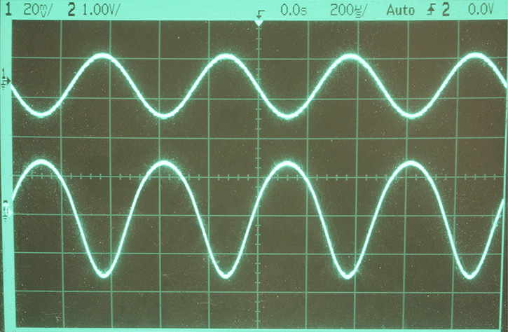
FIGURE 8.26 R1" = 25Ω, Vin = 32 mV peak to peak (top waveform), and bottom waveform Vout = 3 v peak to peak with 12 percent harmonic distortion. Gain ~ –94 = Vout/Vin. Also note the phase inversion between the output signal Vout and the input signal Vin.
To lower output signal distortion R1" is increased to 20kΩ. See Figure 8-27 bottom trace.
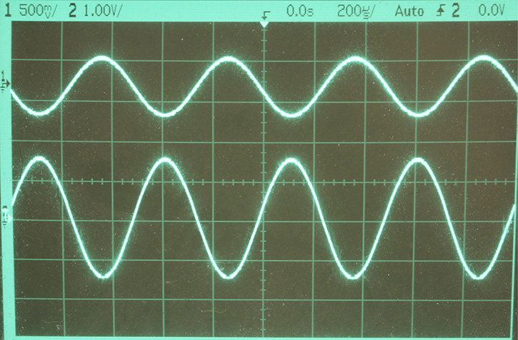
FIGURE 8.27 R1" = 20KΩ, Vin = 720 mV peak to peak (top trace), and Vout = 3 v peak to peak for a gain of – 4.2 (bottom trace). Harmonic distortion measured at 1 percent. Again, note the phase inversion of Vout with respect to Vin.
Another Common Emitter Amplifier
We will now look at another type of common emitter amplifier with a series emitter resistor derived from an LED drive circuit. See Figure 8-28, which shows a constant current source LED drive circuit, and then Figure 8-29, which converts the LED drive circuit into an amplifier.
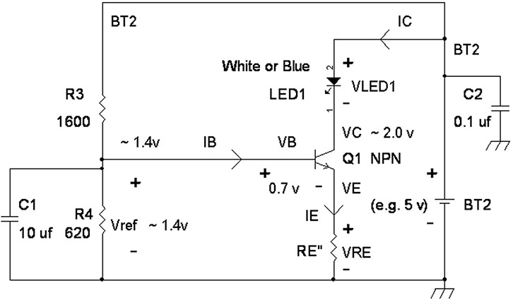
FIGURE 8.28 A constant current source amplifier where the LED drive current = VE/RE".
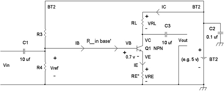
FIGURE 8.29 A simple common emitter amplifier with a series emitter resistor RE".
We can reconfigure the constant current source circuit to an amplifier by replacing the LED with a load resistor, RL, and coupling an input signal voltage to the base with a capacitor. See Figure 8-29.
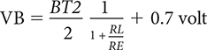
To bias this correctly, generally “Vref” = BT2[R4/(R3 + R4)] is less than half the supply but ≥ 0.5 volts. Typical collector currents can range from 50 μA to about 20 mA for a small signal transistor such as the 2N3904. Generally, the voltage divider resistors ≥ 470Ω, and the emitter resistor RE” that sets the DC collector current can be anywhere from about 100Ω to 10KΩ. Collector current IC = VE/RE", where β >> 1, which is usually the case. In terms of gain, a first approximation has Vout/Vin ~ – RL/(re + RE"), where re = (0.026 v)/IC. Again, this is an inverting amplifier. Generally, it’s harder to provide very high gains from this configuration unless very high supply voltages are used. For example, if we want a gain of –100, and IC = 1 mA, with VE = 1 volt and RE" = 1000Ω, then RL has to be ~100KΩ. This would require BT2 >100 volts. For example, BT2 = 200 volts so that VC is operating at 100 volts DC. Also, a general-purpose transistor will have insufficient breakdown voltage and a high-voltage transistor such as a 2N3439 or MPSA42 would be used instead. If we want instead a gain ~ –10, then we can have RL = 10KΩ, BT2 = 20 volts, Q1 = 2N3904, with VC ~10 volts when IC = 1 mA.
An emitter bypass capacitor CE2 provides higher gain (Vout/Vin) at the expense of higher distortion. But this circuit allows for lower supply voltages. See Figure 8-30.
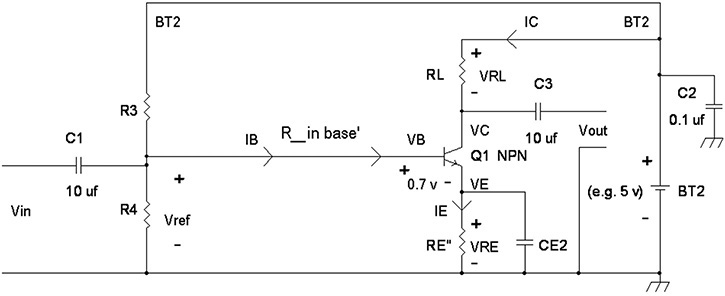
FIGURE 8.30 Capacitor CE2 effectively AC grounds Q1’s emitter.
By adding a resistor (RE2) in series with capacitor CE2, the AC gain can be set without upsetting Q1’s DC bias points (e.g., VB and IC). See Figure 8-31, which includes RE2.
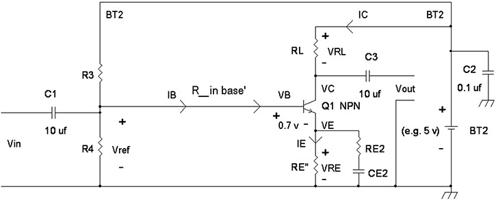
FIGURE 8.31 A second series emitter resistor, RE2, allows for increasing the gain without changing the DC bias conditions. Capacitor CE2 has a large capacitance such that it is an AC short circuit.
In Figure 8-31, with RE2 in series with CE2, the gain G = –[RL/(re + RE" || RE2)], where re = (0.026 v/IC). To find the DC operating points, VC, IC, and VE, we remove the capacitors as shown in Figure 8-32.
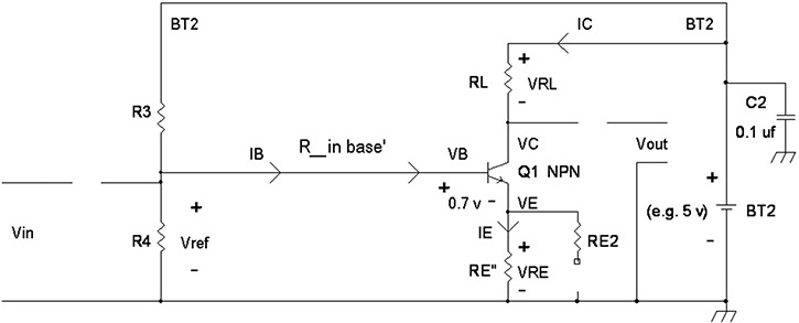
FIGURE 8.32 A DC analysis circuit of Figure 8-31 where capacitors are removed.
With the capacitors removed and neglecting DC base currents due to IB, VB ~ BT2 [R4/(R3 + R4)] and with Q1’s turn-on voltage, VBE ~ 0.7 volt DC, VE ~ VB – 0.7 volt. The collector current IC ~ IE, the emitter current when β >>1, which is usually the case. We now have:
IE = VE/RE"
IC ~ VE/RE"
We now have to also find AC resistance, R_in base, which can be found via IC, β, re, RE", and RE2.
R_in base = β re + (β + 1) (RE" || RE2), where re = (0.26 v/IC).
For the AC analysis model, see Figure 8-33.
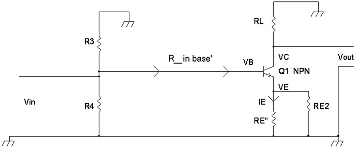
FIGURE 8.33 An AC signal analysis circuit.
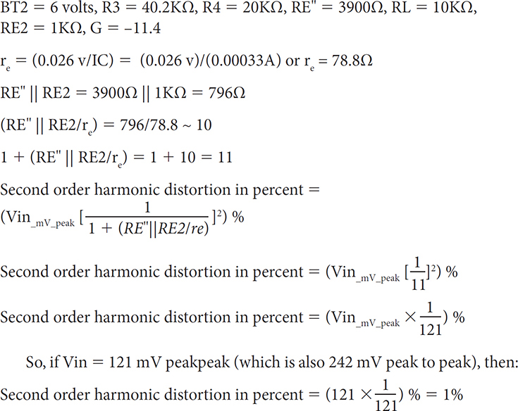
For example, if BT2 = 6 volts, R3 = 40.2KΩ, R4 = 20KΩ, RE" = 3900Ω, RL = 10KΩ, RE2 = 1KΩ, β = 150, then VB ~ 6 v (20K/(40.2K + 20K) ~ 6 v (20/60.2K) VB ~ 2 volts.
VE ~ VB – 0.7 v = (2 – 0.7) v or VB = 1.3 volts. IC ~ VE/RE" = 1.3 v/3900Ω or IC ~ 0.00033A.
To find the gain, G, we calculate for:
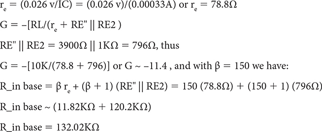
When RE" || RE2 >> re, the emitter resistors RE" and RE2 are the main contributors for R_in base that leads to: R_in base ~ (β + 1) (RE" || RE2).
From Figure 8-34, to find the AC input resistance to the amplifier, it is (R_par || R_in base'), where R_par = R3 || R4. With the example where R3 = 40.2KΩ, R4 = 20KΩ, and the calculated R_in base' = 132.02KΩ, the input resistance is:

FIGURE 8.34 AC signal analysis block diagram with output resistance Ro = RL.
R3 || R4 || R_in base' = (40.2KΩ || 20KΩ) || 132.02KΩ = (13.33KΩ) || 132.02KΩ R3 || R4 || R_in base' = 12.13KΩ
The input resistance = 12.13KΩ.
We can reiterate the gain calculation for G from knowing the collector current and the values of the collector resistor RL and emitter resistors, RE" and RE2 along with re.
The output resistance, Ro = RL, and with RL = 10KΩ in this example, Ro = 10KΩ.
NOTE: An amplifier having a high output resistance such as 10KΩ results in a gain reduction of G when driving a subsequent device (e.g., input stage of another amplifier). If Vout is loading into another device that has an effective 10KΩ to ground will cause the gain, G, drop from –11.4 to half or G → –5.7.
Typical input resistances of audio power amplifiers are between 1KΩ to 100KΩ.
For example, an amplified computer stereo loudspeaker with a 3.5 mm connector has a typical input resistance of 10KΩ.
Troubleshooting the Amplifier in Figure 8-31
1. For measuring the DC conditions, turn off the AC signal source and measure the collector, base, and emitter DC voltages, VC, VB, and VE. Make sure that the transistor is in the amplifying region (forward active region) and not in the saturation region. This can be confirmed by measuring with a DVM that the voltage across the collector and emitter (VCE) > +1 volt DC, or that the collector to base (VCB) voltage > 0.7 volt. Generally, we should expect that VCE or VCB is in the range of at least a quarter of power supply voltage. For example, if BT2 = 12 volts, then VCE ≥ 3 volts. In another example, if BT2 = 5 volts, then the DC voltages across the collector to base (VCB) and across the collector to emitter (VCE) should be ≥ 25 percent (5 volts) or ≥ 1.25 volts.
2. Confirm that R3, R4, RE", and RL are correct. Measure the resistors with the power turned off and with one lead of each resistor disconnected from the circuit. In a special case, you can measure RE2 in circuit because it has a series DC blocking capacitor CE2, but you may have to keep the ohm-meter’s probes across RE2 for about 10 seconds to let the resistance measurement settle.
3. With power turned back on, confirm that the voltages comply with the expected voltage from the voltage divider circuit with R3 and R4. That is, VB = BT2[R4/(R3 + R4)], and VE = VB – 0.7 volt.
4. Confirm that the emitter current is approximately equal to the collector current by measuring the voltage across RL = VRL and voltage across RE" = VRE. Then confirm via calculation from the resistance values of RL and RE" and the measured voltages, VRL and VRE that VRL/RL ~ VE/RE" is within 15 percent if 5 percent resistors are used.
5. If the DC voltages seem unstable, the amplifier may be oscillating at >100MHz. Try inserting a 100Ω series base resistor close to Q1 and see if the DC voltages stabilize and measure to their expected values.
6. With the signal generator turned on having a small amplitude such as 100 mV peak to peak at Vin, measure the AC signal at VE with an oscilloscope. The AC signal at VE should be approximately 100 mV peak to peak within about 25 percent on the low side (e.g., VE’s output AC voltage is in the range of 75 mV to 100 mV peak to peak). Note that the AC voltage at the emitter is the same phase as the base since the emitter terminal acts like having a 0.7 volt DC source voltage between the base and the emitter. A DC voltage source such as the VBE turn-on voltage in series with an AC signal source at the base cannot change the phase of the AC signal at the emitter. The output signal at the collector, VC, should be G × 100 mV peak to peak, or in this example, where G = –11.4, Vout AC should be about 1.14 volts peak to peak that is out of phase with the input signal at the base.
7. In Figures 8-30 and 8-31 emitter capacitors CE and CE2 are chosen to determine the low-frequency response. The 10 μf input and output capacitors, C1 and C3, are designed with sufficient capacitance for most applications with a 20 Hz or lower cut-off frequency. For example, for audio applications, where a low-frequency response of ≤ 20Hz is required, C1 and C3 generally will work because input and output resistances are generally greater than 1KΩ.
For example, the cut-off frequency with a 10 μf capacitor and 1KΩ resistor is:
1/[2π 10 uf (1KΩ)] ~ 16 Hz
To determine the worst-case capacitance values for CE and CE2, choose the low-end frequency you want such as 20Hz. Then use the following formula:
CE or CE2 = 1/[2π fc re]
Let fc = 20 Hz = low-frequency cut-off frequency for an audio application that responds to bass note frequencies.
For example, if IC = 1 mA, then re = (0.026 v/0.001A) or re = 26Ω.
CE or CE2 = 1/[2π 20Hz 26Ω ] = 3.06 × 10⁻⁴ Farad or 306 μf
The closest commercially available value is 330 μf, but to ensure a safety margin just in case, use a 470 μf unit if possible. Since the emitter voltage is generally less than 25 volts, you can use at least a 16-volt electrolytic capacitor. Make sure the (–) terminal of CE or CE2 is grounded.
8. Confirm that any electrolytic capacitors in the circuit are correctly connected (polarity-wise) to avoid reverse biasing. Reverse biasing electrolytic capacitors usually cause the DC bias points to be wrong, due to current leakage through the electrolytic capacitors.
9. The common emitter amplifier in Figure 8-30 where capacitor CE is an AC short circuit from emitter to ground has the same input amplitude limitation as the simple bias circuit in Figure 8-11 for tolerable distortion at the output, Vout. By tolerable distortion, an example would be for intelligible voice signals, < 10 percent harmonic distortion is workable. That is, generally the input signal, Vin, is limited to less than 10 mV or 20 mV peak to peak when driven by a low impedance source signal such as a 50Ω generator. If Vin is driven with a larger value source resistance such as a ≥ 10KΩ series resistor, the distortion will be lower but the voltage gain will be lower as well due to the input resistance forming a voltage divider circuit.
For higher-fidelity applications that require lower distortion at the output less than 1 percent, use the circuit in Figure 8-31. See #10 below concerning distortion calculations.
10. In Figure 8-31 where CE2 is an AC short circuit (e.g., CE = 470 μf), we can estimate the input signal’s amplitude for second order harmonic distortion at the output. Note that Vin_mV_peak is measured in peak amplitude sinewave.
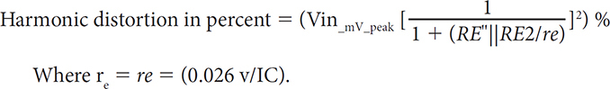
For example, for Figure 8-31:
Vin’s peak to peak voltage for 1 percent second order distortion is then 2 × 121 mV peak to peak or 242 mV peak to peak. This 242 mV peak to peak input level assumes that the output has not clipped. With a gain G = –11.4, the output will be Vout = 2.76 volts peak to peak (11.4 × 242 mV p-p).
Note that the 2nd order harmonic distortion formula is proportion to input level. That is doubling the signal level results in twice the distortion, or halving the input level gives half the distortion at the output.
A safer estimate to ensure that there is no clipping is to reduce Vin to the 0.5 percent level. This is just one half of 242 mV peak to peak input level for 121 mV peak to peak that results in the output.
Vout = 1.36 volts peak to peak for 0.5 percent second harmonic distortion
Maximum Output Voltage Swing
We will now examine how to achieve maximum output swing in differently configured common emitter amplifiers.
Amplifier’s Emitter AC Grounded via CE
The DC collector voltage will determine output voltage swing. For the circuit in Figure 8-30, where capacitor CE is an AC short circuit, the maximum voltage swing will be from VE to BT2. For example, if VB is 2 volts, then VE = 1.3 volts due to the 0.7-volt base – emitter voltage. If BT2 = 6 volts, then the peak to peak output swing will be from +1.3 volts to +6 volts, which will be (6 volts – 1.3 volts) peak to peak or 4.7 volts peak to peak. However, often the DC collector voltage is not centered to give maximum voltage swing without clipping prematurely on one-half of a sine wave cycle before the other half of the sine-wave. To maximize, you can set the DC collector voltage at the average of BT2 and VE, which is VC = (BT2 + VE)/2.
For this example:
VC = (6 volts + 1.3 volts)/2 or VC = 3.65 volts for “symmetrical” clipping
Amplifier’s Emitter Partially AC Grounded via Series RE2 and CE2
In Figure 8-31, we have a little bit more going on because both emitter and collector terminals have AC output signals. Clipping occurs when either the collector voltage approaches the power supply voltage (e.g., BT2), or when the collector voltage matches the (same) voltage at the emitter. That is during the positive sine-wave cycle of the emitter and the negative cycle of the collector matches the voltage across the collector and emitter (e.g., VCE) is approximately 0 volt. Put in other words, the collector voltage equals (or matches) the emitter voltage.
For Figure 8-31 where RE2 is generally > re, the input signal range for “undistorted” output can be approximated when RE" || RE2 >> re as follows: Turn off the input signal and measure DC voltages for VC and VE. Let’s call these DC voltages, VCdc and VEdc. The total collector voltage swinging downward toward the emitter’s voltage is VCdc1ac = VCdc + G Vinpeak and the total voltage at the emitter swinging up toward the collector voltage is VEdc1ac ~ VEdc + Vinpeak.
The input voltage that can be found by the collector voltage equals the emitter voltage:
VCdc1ac = VEdc1ac
VCdc + G Vinpeak = VEdc + Vinpeak
To find Vinpeak, this can be summarized as:
Vinpeak = (VCdc – VEdc)/(1 – G)
A step-by-step calculation is now shown.
For example, BT2 = 6 volts, RL = 10KΩ, R3 = 40.2KΩ, R4 = 20KΩ so
VB = BT2 [R4/(R3 + R4)] = 6 volts [20K/(40.2K + 20K)] = 6 volts [20K/60.2K]
VB ~ 6 volts [2/6] or VB ~ 2 volts. IC ~ VE/RE" = (VB – 0.7 volt)/3900Ω or
IC ~ 1.3 v/3900Ω or IC = 0.00033 A. This makes VCdc = 6 volts – IC(RL) or:
VCdc = 2.7 volts. VEdc = VB – 0.7 volts = 2 volts – 0.7 volt = 1.3 volts
VEdc = 1.3 volts
We need to equate VCdc1ac = VEdc1ac to find the maximum peak voltage swing at clipping.

In practice both Vinpeak and Voutpeak will be slightly smaller to avoid clipping or distortion.
Finding an Optimum Bias Point for Maximum Output Swing with Just an Emitter Resistor
With a common emitter amplifier with just a series emitter resistor (e.g., RE) and where the series emitter resistor >> re = (0.026 v/IC), we can find an optimal bias voltage based on the collector load resistor, RL and series emitter resistor, RE. See Figure 8-35.

FIGURE 8.35 A common emitter amplifier with an emitter series resistor, RE.
To find an optimal biasing voltage, VB, given the values for RL and RE, we have:

For example if we want to make a unity gain phase splitter amplifier where amplitudes of the AC signals are about equal via the collector and emitter terminals (Vout and Vout2), RL = RE.
NOTE: For a phase splitter amplifier circuit, output terminals Vout and Vout2 are generally loaded with equal resistance values of at least 10 x RL.
If BT2 = 12 volts, and RL = RE = 1KΩ, then:
VB = 3 v + 0.7 v or VB = 3.7 volts
This would mean VE = VB – 0.7 v or VE = 3 volts.
If there is a 3-volt drop across RE, then there should be a 3-volt drop across RL since RE = RL, given that the emitter current = collector current for β >>1. That is VRL = VRE.
Thus, VC = BT2 – VRL = BT2 – VRE = 12 v – 3 v or VC = 9 volts.
This makes sense because at VE = 3 volts, the maximum swing at the emitter is 3 volts ± 3 volts or 0 volt to 6 volts at the emitter. If there is 6 volts at the emitter for VE, then the collector voltage is VC = BT2 – VRE = 12 v – 6 v, or VC = 6 volts. This then satisfies the condition that maximum swing is when the collector and emitter voltages are equal.
In practice the collector-to-emitter voltage is rarely 0 volt but close, such as 0.2 volt. And this will reduce the maximum calculated swing by a slight amount. But this equation is fine for a first approximation.
With RL = RE = 1KΩ, and BT2 = 12 volts, here are example resistor values for R3 = 39KΩ and R4 = 18KΩ. And we can confirm that VB is close to 3.7 volts.
VB = 12 v [R4/(R3 + R4)] = 12 v [18K/(39K + 18K)] = 12 v [18K/57K]
VB = 12 v [0.3158] or
VB = 3.789 volts ~ 3.7 volts
Because RE = 1KΩ and R3||R4 < 20RE → 39KΩ || 18KΩ < 20KΩ = 20RE, we can use a transistor of β ≥ 100 such as a 2N3904.
Summary
The amplifiers presented have limitations in terms of input amplitudes and output swing. Distortion can be a problem unless there is a series input resistor or a series emitter resistor that reduces gain and distortion. Be aware of the capacitors’ capacitance values at the input, at the output, and especially connected to the emitter (e.g., CE and CE2), which will determine the amplifier’s low-frequency performance.
Also, make sure electrolytic capacitors are biased correctly; otherwise, they will be reverse biased. Having electrolytic capacitors wired backwards results in leakage currents that will cause the expected DC bias points to shift up or down. You can use a voltmeter to confirm the correct polarity voltage across the electrolytic capacitors.
This concludes Chapter 8 concerning simple one-transistor amplifiers. In Chapter 9 we will explore some linear integrated circuits such as operational amplifiers and voltage regulators.