From basics to ASICs, we’ve covered a lot of ground in Chapters 1–5. We started with foundational electronic physics and transistor structure, then focused on how semiconductors are designed, manufactured, and integrated into larger systems. Though our discussion has helped us build a holistic model of electronic systems, thus far it has largely treated semiconductors as a monolith devoid of differentiating features. In this chapter, we will break apart this monolith, exploring the numerous types of common circuits and system components that comprise the semiconductor family. Before we explore each of these major subcategories, we’ll first explore the differences between digital and analog technology.
Digital vs. Analog
There are two main types of components that get their names from the type of signals that they use – digital and analog. Digital signals act like a light switch – they are either on (1) or off (0) (MPS, n.d.). These patterns of 1’s and 0’s are used to convey information and constitute the binary computer language that most people are familiar with when they think of electronics (MPS, n.d.). Digital signals are usually also synchronous – they run on a reference clock to coordinate the processing of different functional blocks and ensure proper timing (MPS, n.d.). Though their predictability and synchronous timing make them great for storing and processing information, digital circuits are unable to transport information over any sort of distance without physical wiring to move their signals from place to place.

A diagram exhibits sine wave and square wave patterns labeled analog signal and digital signal, respectively.
Analog vs. Digital Signals
Analog signals are distinguished from one another by their frequency. Frequency describes the number of times an analog signal wave completes an up and down cycle, or repeats itself, over a fixed period. For a given signal, frequency is inversely proportional to wavelength and directly proportional to power – the greater the frequency, the shorter its wavelength, but the greater its energy level (NASA Hubble Site, n.d.). To remember this dynamic, I find it helpful to picture an exhausted parent taking their restless child to the park after a long day of work. The child running around the park may be smaller but has much more energy and higher frequency of movement than their larger parent, who lumbers from swing set to monkey bars. Electrical frequency is measured in units called Hertz (Hz), which describes the number of times an electromagnetic signal completes an up-down cycle per second (Encyclopædia Britannica, n.d.). The unit Hertz is named after Heinrich Hertz, a German physicist who performed early research into properties of electromagnetic radiation. By receiving and processing different frequencies, analog electronics can perform all kinds of useful things from detecting external stimuli (sensors) to wireless data transmission and communication (RF technology).

A diagram exhibits two wave patterns, one with long wavelengths, low frequency, and low energy, and one with short wavelengths, high frequency, and high energy.
Wavelength vs. Frequency vs. Energy
Analog vs. Digital Signals
 A table has 2 columns and 6 rows. The column headers are analog and digital. The row headers are signal structure, representation, signal integrity, transmission medium, power requirements, and examples. A table has 2 columns and 6 rows. The column headers are analog and digital. The row headers are signal structure, representation, signal integrity, transmission medium, power requirements, and examples. |
Common System Components – The SIA Framework
So we now know that there are two types of components – digital and analog – but what do all of these components do? When building a system, designers and architects have a multitude of individual parts to choose from, each with its unique advantages and disadvantages. Driven by demand in the six end-use markets (communications, computing, consumer, automotive, government and industrial electronics), the component market is diverse and highly competitive. The variety of individual products and devices can be daunting, so it’s helpful to use the Semiconductor Industry Association’s framework, breaking the market into five constituent segments (SIA, 2021).
1. Micro Components (Digital): Micro components include all non-custom digital devices that can be plugged into another system and used for computation or signal processing. You can think of them as generic subcomponents and specifically include microprocessors, microcontrollers, and digital signal processors (DSPs) (SIA, 2021).
2. Logic (Digital): Logic encompasses all non-micro component digital logic. This segment primarily refers to specialized circuitry and includes application-specific ICs (ASICs), field programmable gate arrays (FPGAs), and more versatile, but application-specific digital logic devices (SIA, 2021).
3. Memory (Digital): Memory is used to store information and is usually classified based on whether it can store data with or without power. Volatile memory (RAM) requires power to store memory, but enables quicker access, while non-volatile memory (ROM) can retain memory without access to power. Dynamic random access memory (DRAM) is the most common type of volatile memory, while NAND flash is the most common type of non-volatile memory (NAND is not actually an acronym, but rather stands for “NOT AND”, a type of boolean operator and logic gate) (SIA, 2021).
4. Optoelectronics, Sensors and Actuators, and Discrete Components – OSD (Analog and Digital): Optoelectronics include laser devices, display technology, and other photonics-based electronics. Sensors include all kinds of specialized devices used to measure everything from temperature to air pressure. Actuators include devices that initiate movement or take other actions in response to a stimulus detected by a sensor (SIA, 2021). Discrete components are individually packaged, specialized transistors or other basic components, like resistors, capacitors, and inductors.
5. Analog Components: Analog ICs process analog signals and are classified as either standard linear integrated circuits (SLICs) or application-specific standard products (ASSP). SLICs are generic, plug-and-play analog devices that can be integrated into a larger system. ASSPs are components designed for a specific application, but can still be integrated into multiple systems within that application category. As we discussed in the last section, analog electronics process real-world signals like radio waves, light, sound, temperature, and other sensory signals.

A horizontal bar chart represents the sales of nine products in billions of dollars. Logic leads at 118, followed by memory at 117, analog at 56, M P U at 52, opto at 40, discretes at 24, M C U at 15, sensor at 15, and D S P at 2.
2020 Distribution of Semiconductor Sales by Component Type (SIA and WSTS)
Micro Components
Microprocessors and Microcontrollers
In its simplest form, a processor is a chip that receives input, processes said input, and produces an output that can be used for some intended purpose. The term microprocessor (MPU) is generally used to describe more complex digital circuits, like CPUs, that connect to a larger system. They perform a general computing function and require an external bus to connect to memory and other peripheral components (Knerl, 2019).
While microprocessors handle general computing tasks, microcontrollers perform specific functions and are integrated with memory and I/O connections all on one chip (Knerl, 2019). Generally, microcontrollers are smaller, less powerful processors that can serve as plug-and-play computing power for simple operations (Knerl, 2019). They are used widely in low power IoT devices and embedded systems. PCs and Servers account for the largest share of microprocessor sales, while automotive, industrial, and computing account for most sales in the microcontroller segment (SIA, 2021).
It is important to distinguish microprocessors and microcontrollers in the Micro Component segment from processors in the Logic segment. Logic devices are custom designed for a specific application, while Micro Components provide more generic processing that can be combined with other components in all kinds of systems (Schafer & Buchalter, 2017).
Digital Signal Processors (DSP)
Digital signal processors (DSPs) are used to process multimedia and real-world signals like audio, video, temperature, pressure, position, etc. (Analog Devices, n.d.). Digital electronics have trouble accurately representing the real world in 1’s and 0’s, so they need DSPs to make sense of them in a way they can understand. They are usually fed converted analog signal data from an Analog-to-Digital Data Converter (ADC) for quick processing, before sending their output to other processors or back out into the world through a Digital-to-Analog Converter (DAC), depending on the application (Analog Devices, n.d.). There’s a DSP in your mobile phone, for example, that enables modes like Bass Boost to change the nature of the sound coming out the headphones. DSPs are adept at high-speed, real-time data processing and are highly programmable, which makes them easy to implement in a wide variety of devices and systems (Analog Devices, n.d.).
Micro Component Market Summary

A pie chart has 6 slices. Computing holds the biggest slice at 57%, followed by industrial at 14%, automotive and communications at 11% each, consumer at 7%, and government at 1%.
2020 Microprocessors, Microcontrollers, and Digital Signal Processor Market by End Use (SIA and WSTS)
Logic
Special Purpose Logic
Special Purpose Logic encompasses all ICs designed and sold as standard products. This includes a range of specific ICs, including wireless controllers like Ethernet and WLAN, Modem SoCs, image and audio processors, PC Core Logic, and GPUs (SIA, 2021).
Special Purpose Logic Devices are Application-Specific Standard Parts (ASSPs) that are designed and integrated into a system the same way Application-Specific Integrated Circuits (ASICs) are (Maxfield, 2014). The term “standard parts” here just means that the same part can be used in many different products. For example, the same “standard” 12-bit video DAC (Digital to Analog Converter) can be used on a Ring doorbell, an LCD TV, or a handheld game console. A “custom” part is specifically designed for a single device. High-volume consumer products like iPhones utilize many different custom chips – when you’re selling hundreds of millions of iPhones, it's worth it to squeeze every last bit of performance using specialized silicon. The main difference between the two is that ASICs are designed and optimized for a specific use in a single system (i.e. Samsung designs an ASIC CPU for its smartphone or AMD designs an ASIC GPU to power Microsoft’s Xbox video game systems) as opposed to a more generalized application (Intel designs a server-based CPU aimed at all Data Center customers) (Maxfield, 2014). Standardized product types such as Input/Output (I/O) circuits like USB or PCIe are also classified as ASSPs (Maxfield, 2014).
Central Processing Unit
Central Processing Units (CPUs), as the name implies, are the main processing center for most computing systems (Encyclopædia Britannica, n.d.). They are a type of microprocessor and are likely the first thing that comes to mind when you think of a computer’s inner workings, but don't let the term CPU limit your thinking to the computer on your desk, or the laptop in your bag – from smart speakers to automotive control systems, any device that processes information can have a CPU. There might even be a CPU in your coffee maker.
You can think of a CPU as the digital “brains” of a computer, processing and executing instructions as needed. The core processing of a CPU is handled by something called the Arithmetic Logic Unit (ALU), which performs numerical and logic-based operations necessary to run all the software it was intended to deliver (Fox, n.d.). CPUs are complicated circuits and can house billions of transistors on a single die.
CPUs are typically connected with other modules through a bus or chipset that feeds information into the CPU for processing and directs output data to memory for storage or to other system components (Thornton, 2016). To connect with other memory chips holding instructions awaiting processing, CPUs use registers as the physical entry and exit point for data flow to and from the rest of the system. Instructions and data must enter and exit through these registers, which act like an “information security team” keeping unauthorized people from getting into a club or private party. Each CPU has a fixed number of registers through which data can flow, with typical register capacities measuring 8-, 16-, 32-, or 64-bits “wide” (Thornton, 2016). These numbers indicate the number of bits a CPU can access from its memory at a given time. If a CPU is a water tank, its register bit count indicates the diameter of the hose used to fill it up or empty it out.
An individual microprocessor in a CPU or GPU may be referred to as a core, which can be combined with other “core microprocessors” to tackle complex tasks and run more taxing applications (Firesmith, 2017). When computer manufacturers advertise their powerful, multi-core architecture – this is what they are referring to.
Together, the CPU and other components are “integrated” onto a single IC (SoC) or a larger system. One laptop may include a separate CPU, memory, GPU, power source, and multimedia processors, while another may integrate all of these onto a single SoC or Multi-Chip-Module (MCM).
Intel is a leader in developing CPUs that power devices like personal laptops, though many other companies like AMD develop CPUs as well.
Graphics Processing Units

A diagram exhibits the differences between the C P U and the G P U via a 4 by 4 block and an 11 by 11 block, respectively. Each has a bulleted list of 5 steps.
CPU vs. GPU
Some of the more recent and exciting applications of GPUs are in artificial intelligence and machine learning (Dsouza, 2020). Deep learning and other AI techniques require the execution of multitudes of relatively simple arithmetic calculations. Machine learning involves lots of computation of two-dimensional arrays of numbers, called matrices. When you think about it, a computer display is just a big matrix of individual pixels, so it was natural to look to GPUs as the ideal matrix processors. And because GPUs can break down complex problems into smaller, constituent problems, they are well equipped to handle the millions and billions of small trial-and-error calculations necessary to deliver arduous AI solutions (Dsouza, 2020). That same number-crunching power that makes GPUs good at machine learning also makes them good at mining cryptocurrencies. GPUs can complete the hash operations of cryptocurrency mining much faster than a CPU. In fact, the same way companies created custom GPUs for graphics years ago, companies are now creating processors custom-built just for cryptocurrency mining.
While most of the semiconductor industry has been consolidating, innovations in AI-centric GPUs have led to a significant growth area where new companies have been able to compete. Specific applications ideal for GPU processing include autonomous driving, machine vision and facial recognition, high performance computing (HPC), complex simulation and modeling, data science and analytics, bioinformatics, and Computational Finance, to name a few (NVIDIA, 2020).
ASICs vs. FPGAs
ASICs and FPGAs represent two different approaches to chip design and development, each with their own pluses and minuses.
ASIC stands for Application-Specific Integrated Circuit. As the name implies, ASICs are designed for a specific purpose (Maxfield, 2014). By designing a chip from the ground up, ASICs have several performance advantages including high speed, lower power consumption, smaller area, and lower variable manufacturing costs at high volumes (Maxfield, 2014). The main drawback for ASICs is the significant upfront development costs that go into their design (Cadence PCB Solutions, 2019). Building a chip is a capital and labor-intensive process that requires teams of highly qualified and well-paid engineers. Even if a chip is taped-out (finished) and sent to the fab for manufacturing, there is always the risk that yields are low, or that the ASIC does not function as intended. No amount of verification, validation, and failure analysis can eliminate the risk of serious flaws, and this risk must be considered when deciding whether developing an ASIC makes sense.
Another drawback of ASICs is that they are typically so customized for a given application that they can’t be used in another area. For example, audio devices use digital-to-analog converters (DACs) to convert digital voice or music data which is driven as an analog signal to a speaker. The DAC driving the speaker in your phone is customized for the frequency and performance levels needed for audio. That same DAC can’t be used to convert the digital video signals to drive the LCD screen. Each application needs a different chip, which adds to cost and complexity.
FPGA stands for Field Programmable Gate Array. As the name implies, these chips are “programmable,” which means they can be customized to serve a specific function after they have already been manufactured (Cadence PCB Solutions, 2019).
Most FPGAs can, in fact, be erased, then “re-programmed” to serve a new purpose, which makes them ideal for prototyping new designs (Cadence PCB Solutions, 2019). An engineer can program an FPGA with a new design, test how it functions in the real world, and iterate from there to perfect their design before moving it to manufacturing. This programming step can be performed in minutes, compared to months or years to design and manufacture an ASIC. Devices called emulators are essentially a box with a bunch of FPGAs working together that allow ASIC designers to iterate their designs before moving to manufacturing (Xilinx, n.d.). Emulators are becoming more and more important as chip manufacturing costs increase. Fine-geometry processes can cost millions of dollars for the first tape-out of a new custom chip, so it's critical that the design is correct. Emulation is a way to further verify how a given design performs in the real world and be sure it will function correctly when it comes back from the fab. We can see the various applications FPGAs are used for in Figure 6-6.
While ASICs can take as much as a year to design and cannot be reprogrammed after manufacturing, FPGAs offer “off the shelf” solutions that enable companies to quickly bring a chip to market, albeit at a much higher per-unit price point (Cadence PCB Solutions, 2019).

A spoke diagram exhibits consumer electronics, video and image processing, security systems, scientific instruments, wireless communications, aerospace and defense, and medical electronics as F P G A applications.
Potential Applications of FPGAs
ASIC or FPGA – Which to Choose?
A key decision for many companies in need of an IC is whether to build a custom ASIC or use an off-the-shelf FPGAs. At the crux of the dilemma is a trade-off between performance and price. ASICs can take months or years to develop and cost well into the millions, even billions of dollars, in upfront R&D with no guarantee that the finished product will perform as intended (Trimberger, 2015). Because of their custom design, however, ASICs have considerable speed and power efficiency advantages over FPGAs that still must perform programmed tasks while carrying extra circuitry “dead weight” that isn’t needed for its programmed application.
If you are working with short time-to-market constraints or lower-than-expected manufacturing volumes, FPGAs are usually the better choice, assuming there is some wiggle room for poorer performance (Trimberger, 2015). As expected volumes increase, however, the per-unit cost of ASICs becomes increasingly attractive (Trimberger, 2015). At higher volumes, high up-front development costs can be spread out over a greater number of units, capitalizing on long-term yield improvements, reducing net spend on materials, and costing companies less per device (Trimberger, 2015). For this reason, most companies with high product volumes and stringent performance requirements have invested in developing custom ASICs, either by partnering with a fabless design company like Qualcomm or by developing them in house. Apple, Facebook, Google, and Tesla all develop custom ASICs for their devices for example.

A line graph represents total cost versus volume. A S I C and F P G A exhibit rising trends from and to different coordinates, with their intersection marking the point where the former becomes cheaper than the latter.
FPGA vs. ASIC Cost Analysis

A table has 2 columns and 6 rows. F P G A has the advantage in time to market, unit costs at low volume, and low barriers to entry, while A S I C has the advantage in performance, unit costs at high volume, and energy efficiency.
FPGAs vs. ASICs – Advantages and Disadvantages
System on Chip
System on Chips (SoCs) are a complex and highly integrated type of ASIC that can house billions of components on a single silicon chip. As the name implies, SoCs contain an entire functional device all on one IC substrate – a single unit may have a CPU, memory, GPU, power management unit, wireless circuitry, and other components or functional modules. To be considered an SoC, an IC must have at a minimum, microprocessors and/or microcontrollers, DSPs, on-chip memory, and peripheral functions like hardware accelerators (Maxfield, 2014).
For larger devices with greater power accessibility like PCs, design teams may have plenty of space and flexibility to design the system with distinct modules, perhaps deciding to integrate the system at the package level with MCM. For smaller applications like cell phones, however, multiple chips may require too much space and power. Tighter integration mitigates these problems, enabling engineers to fit entire computing systems in the palm of your hand. SoCs are used pervasively in mobile devices like cell phones, tablets, smartwatches, and other battery-powered devices where space and power are limited. Though SoCs are used most in embedded and mobile devices, they have been increasingly used for laptops and other devices that can still leverage their performance advantages.

A diagram exhibits the similar components of A S S P and A S I C, except for the former's general purpose for many companies or many systems and the latter's special purpose for 1 company or 1 system.
ASIC vs. ASSP
Logic Market Summary

A pie chart has 6 slices. Communication holds the biggest slice at 44%, followed by computing at 25%, consumer at 15%, automotive at 7%, industrial at 6%, and government at 2%.
2020 Logic Market by End Use (SIA and WSTS)
Memory
Since the birth of the electronics industry in the 1960s and 1970s, the market needs for data storage has skyrocketed, driving demand for more advanced memory chips to new heights year after year.
Memory Stack
Memory’s primary function is to store data and information for use in the processing centers of larger systems (Nair, 2015). Storage capacity is no longer the dominant performance constraint for many of today’s advanced memory devices. Over the past decades, the bridge between memory and the core system processors has instead become a key bottleneck for device performance, driving the development of new memory chips and microarchitectures (Nair, 2015). Getting the data in and out of the memory is now the critical parameter. Extra memory capacity is useless if your processor can’t retrieve and deliver information faster than it can process the data you’ve stored.
Instruction, data, and information flow between the CPU and the memory stack starts with an input source and flows through the memory hierarchy for processing and storage. This input stimuli could range from a command typed into a keyboard or the click of a mouse to a signal released by a sensor triggered by stimuli from the external environment – this could be sound captured by a speaker (“Hey, Alexa”), movement detected by your home security camera, or a swipe on your smartphone screen. The input triggers core instructions to be readied by the long-term, non-volatile ROM memories, which are then sent to volatile RAM memories higher up in the stack (closer to the CPU) (Tyson, n.d.). These instructions are quickly transferred to Level 1 and Level 2 cache memories, which directly interfaces with the CPU registers (Tyson, n.d.). These cache memories store data and instructions for quick access. Through a data bus, the level 1 cache delivers the instructions and necessary data to the CPU, which processes it and returns output instructions that can either be held in up-stack cache for quick re-use or delivered to down-stack permanent storage for another time (Thornton, 2016).
In designing memory architectures, system designers are always balancing the competing constraints of memory capacity and access speed. Massive, dense memories can deliver all the capacity you could possibly desire, but searching for and retrieving the information you need will be slower. This is why designers use a memory hierarchy, with smaller, faster cache memories used to store frequent, time-sensitive operations that can be accessed quickly, and larger but slower memories used to store broader datasets that are needed less often.
Memory can be classified into two broad categories, temporary storage volatile memory and permanent storage non-volatile memory (Shet, 2020). The first important distinction between the two is that volatile memories require power to store data, while non-volatile memories do not (Shet, 2020). Once power is removed to volatile memory, all the data is lost. Permanent storage non-volatile memory is used for operations that never change – like the booting instructions your computer uses to turn on. Volatile memory, on the other hand, is used for operations that underlie any programs or applications you might be running. When you turn on your computer, it’s using non-volatile memory, and when you open the web browser, it’s using volatile memory. The second important distinction denotes each memory’s read/write ability – RAM (Random Access Memories) allow a processor to both read or “take” input data and write or “deliver” output data to memory, while ROM (Read Only Memory) can only be programmed once and cannot be easily re-purposed (Shet, 2020). You can think of RAM like a white board that you can read from or write on until you need to write something else, while ROM is more like a diary that is not particularly useful once you run out of pages.
ROM vs. RAM
 A table has 2 columns labeled R O M and R A M. Each has 6 rows with non-volatile, no power, more storage, long-term memory, start-up functions, and slow data transfer for the former and the opposite for the latter. A table has 2 columns labeled R O M and R A M. Each has 6 rows with non-volatile, no power, more storage, long-term memory, start-up functions, and slow data transfer for the former and the opposite for the latter. |

A pyramid chart exhibits the components of external I O, R O M under long-term storage or non-volatile memory, R A M slash D R A M slash S D R A M and cache under short-term storage or volatile memory, and C P U.
Memory Hierarchy

A diagram exhibits more storage but slower and vice versa states of various C P U components. On the right are 4 sequential illustrations of a person picking up a book from a library to use as a source for his assignment.
Memory Hierarchy Library Analogy
There are numerous kinds of volatile and non-volatile memories available. We cover them in the following sections.
Volatile Memory
The most common types of volatile memories are DRAM and SRAM. As random-access memories, they function as the CPU’s short-term memory, allowing it to quickly access and process information (Shet, 2020). DRAM (Dynamic Random-Access Memory) can hold more data than an SRAM (Static Random-Access Memory) but is slower overall (Shet, 2020). SRAM may have faster access speeds but requires more power to function properly – a perfect example of the trade-off between performance and power (Shet, 2020). This differential is due to the number of storage transistors each has – SRAM has six transistors to hold data locally, while DRAM only has one.
The RAM memory closest to a CPU or processor is called RAM Cache, or CPU Memory, often referred to simply as cache. Cache has the greatest speed requirement of any memory type and typically stores instructions waiting to be executed (Shet, 2020). Because of its speed advantage, SRAM is often used as cache, while DRAM, which has greater capacity and lower power requirements, is more frequently used as temporary working memory (Nair, 2015). In the library-backpack analogy, if the student waiting to process information is the CPU, then the cache would be an individual book on the desk, waiting to be read.
In addition to cache-level data transfer rates, computing speeds are also limited by the transfer speeds between memory DRAM and cache (Shet, 2020). During each clock cycle, a fixed amount of data can be transferred between DRAM and cache. On its own, the limited transfer speed of even traditional DRAM would be a significant processing bottleneck. To mitigate this issue, a technology called DDR (Double Data Rate RAM) or DDR SDRAM was developed. Compared with prior DRAM generations, DDR has greatly increased the speed of data transfer, boosting connectivity between DRAM and cache. Big picture, it’s less important to know the technical nuances of the various flavors of DRAM and SRAM, as much as it is to understand RAM as a category and how it relates to other parts of the memory hierarchy.
Non-Volatile Memory
There are two types of non-volatile memories – primary memory and secondary memory. All RAM memories are considered primary, while some read-only memories (ROMs) are classified as secondary. Primary memories are the main working memories of a computer – they can be accessed more quickly by the processor, but have limited capacity and are usually more expensive. Secondary memories, also known as Backup or Auxiliary memories, can only be accessed through interconnects and are much slower. You can think of primary memories like the space at a storefront with all the inventory you need to do business day to day and secondary memories like cheap warehouse space where you store everything else. You may bring new inventory to the store from the warehouse when needed, but don’t have the budget or the floor space to keep it all at once.
Primary Non-Volatile Memory
Standard ROM cannot be adjusted or rewritten and must be programmed when it is created (Shet, 2020). The data is literally hard-wired when the chip is manufactured.
PROM (Programmable Read-Only Memory) can be programmed after manufacturing but cannot be changed once programmed. PROM is essentially ROM that is programmable a single time through a process called burning (Shet, 2020).
EPROM (Erasable Programmable Read-Only Memory) addresses most of the issues with ROM and PROM and can be erased and re-written many times (Shet, 2020). To erase EPROM, however, requires a special tool that uses the energy of UV light to destroy stored data without destroying the underlying electronics. Unfortunately, this method does not allow for selective erasure and the whole EPROM must be re-written before re-use (Shet, 2020).
EEPROM (Electrically Erasable Programmable Read-Only Memory (Try saying that five times fast!) tackles some of the issues with EPROMs. Namely, the whole chip does not have to be erased and no UV-light tool is required to erase the EPROM (Shet, 2020). The main drawback of EEPROM is that they must be changed one byte at a time, making them relatively slow to erase and re-program. This slow erasing speed led to the final type of ROM, NAND Flash.
NAND Flash Memory is a type of EEPROM that overcomes the limits of other types of ROM. It can erase information, write data in chunks (as opposed to one byte at a time) and works considerably faster than EPROM (Shet, 2020). Flash NAND is the primary type of ROM used to store data in electronic devices today (Shet, 2020).
Secondary Memory (HDD vs. SSD)
Secondary memories are external non-volatile RAM memories used for permanent storage and core device functions like boot drive. The most common types of secondary memory are Hard Disk Drives (HDD) and Solid State Drives (SSD). Hard Drives are built from a magnetic disk with a read/write arm that can store data indefinitely (Brant, 2020). An SSD performs a similar function but uses interconnected NAND Flash memory chips instead of a disk (Brant, 2020). NAND Flash memories are faster and more reliable than HDDs but are more expensive and have lower capacity (Brant, 2020). Moore’s Law, however, is making NAND Flash cheaper and denser every year. That cheap, dense Flash memory has made all our portable electronics possible – imagine if your cell phone needed a spinning hard drive platter to function!
HDD vs. SSD
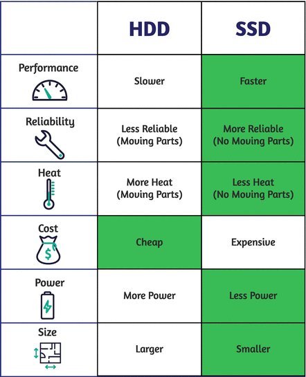 A table has 2 columns labeled H D D and S S D and leftmost rows labeled performance, reliability, heat, cost, power, and size. S S D has the advantage in all but cost. A table has 2 columns labeled H D D and S S D and leftmost rows labeled performance, reliability, heat, cost, power, and size. S S D has the advantage in all but cost. |
Stacked Die Memory (HBM vs. HMC)

A diagram exhibits the H B M structure via a stack of 4 memories atop device logic and a C P U forward slash G P U + host logic on a platform, and the H M C structure via a stack of 4 memories atop logic.
High Bandwidth Memory (HBM) vs. Hybrid Memory Cube (HMC)
Memory Market Summary

A pie chart has 6 slices. Computing holds the biggest slice at 52.50% followed by communications at 31.67%, consumer at 10.68%, industrial at 2.76%, automotive at 2.35%, and government at 0.04%.
2020 Memory Market by End Use (SIA and WSTS)
Optoelectronics, Sensors and Actuators, Discrete Components (OSD)
Optoelectronics

A diagram exhibits quantum computing, data centers, high-performance computing, telecommunications, consumer goods, sensors and bio-sensors, and aerospace and high end as S i P h applications.
Photonic and Optoelectronic IC Applications
Sensors and Actuators
At their most basic level, sensors detect real-world inputs (heat, pressure, light, sound, or other physical phenomena) and convert them into electrical signals. They can be classified as either active, which require an external power source to function, or passive, which require no power to generate output (GIS Geography, 2021). While sensors these days are mostly active devices with many onboard chips, you do still see passive sensors still being used for select applications, like old-fashioned mercury thermometers. Sensors are often used in control systems, like altimeters used to adjust airplane flight patterns or proximity sensors that trigger a car's automatic braking system. All kinds of semiconductors are used in sensors for a multitude of applications, including optical sensors, pressure sensors, gas sensors, speed sensors, weight sensors, among others (Teja, 2021).
Actuators are like reverse sensors – they revert electrical signals back into real world outputs. Actuators are primarily used in industrial and manufacturing applications like robotics but are beginning to see applications in consumer and automotive markets as well.

A diagram exhibits various sensors and actuators on the back, and some on the front, of an electronic device such as a gyroscope and an auto-focus actuator on the camera module.
Mobile Device Sensors and Actuators (IntelFreePress, 2013)
MEMS

Two photographs of the connected gears and other components of micro-electro-mechanical systems.
MEMS Up Close (Sandia National Laboratories, n.d.)

A spoke diagram exhibits pressure sensing, positional and inertial sensing, optical transmission, biological and medical, power and energy technology, and R F and wireless transmission as M E M S and sensor applications.
MEMS and Sensor Applications
Discrete Components
Discrete components are high volume, individually packaged components used as enabling devices for more complex systems. They generally help route signals and power to different processing centers in a given device. Common discrete components can vary from simple resistors, capacitors, and inductors, to more complex power transistors, switching transistors, diodes, and rectifiers.
Discrete Components vs. Power Management ICs (PMIC)
Power delivery used to be handled exclusively by discrete components that performed functions like voltage regulation, power conversion, battery management, and so on. Power management involves high voltages and signals moving around at high frequencies which can create massive interference issues. Integrating this function onto an IC alongside critical sensors is a difficult problem. But technology is always advancing, and the quest for greater integration and efficiency has led to growth in PMICs and PMUs.
PMUs (Power Management Unit) are a type of microcontroller specific to digital devices. PMICs and PMUs help convert power to a usable form, regulate battery usage and charging, and convert control voltage and flow of electricity to other components in the system like the CPU, memory, and more. Tighter integration does not come without costs, however – clustered components experience higher parasitics (unwanted interference from other components) and other power integrity issues (Texas Instruments, 2018). When a “noisy” power management chip is placed next to a sensitive circuit like a microphone, for example, it can cause performance issues and reduce audio quality. Upfront design costs are higher for PMICs, but their overall performance advantages and efficiency improvements often make PMUs a competitive long-term option.
PMICs are integrated circuits used for a family of chips and modules that are responsible for regulating power and voltage in a system or device (Intersil, n.d.). Typically, unique components in a system require different voltages to operate effectively – 1.0V for processors and memory, 1.8V for interface drivers, and 2.5V for power devices is common. A PMIC ensures that each of these system components receives the correct voltage level according to its unique requirements.
Optoelectronics, Sensors and Actuators, and Discrete Components Market Summary

A pie chart has 6 slices. Communications holds the biggest slice at 32% followed by industrial at 23%, automotive at 22%, consumer at 14%, computing at 9%, and government at 1%.
2020 OSD Market by End Use (SIA and WSTS)
Analog Components
While digital chips have come to dominate for processing and storing information, as we will see in the Wireless Technology Chapter, our physical world is still “analog,” requiring specialized analog chips to help make sense of it. These devices include sensors, wireless technology, and power supplies.
General Purpose Analog ICs vs. ASSPs
There exist two types of Analog circuits: general purpose analog ICs and application-specific standard products (ASSPs). General Purpose Analog ICs are used as broad plug-and-play analog components that may be optimized to perform a specific function, but can be used across many different systems, much like the Micro Component segment on the digital side. They include comparators, voltage regulators, data converters, amplifiers, and interface ICs (WSTS, 2017). In complex systems, these General Purpose Analog ICs frequently sit between an analog sensor and a processor, amplifying and converting the analog sensor signal into a digital signal for use by the processor.
Analog Application-Specific Standard Products (ASSPs) are Analog ICs designed for a specific application, similar to the Logic segment of the SIA Framework. Many ASSPs have digital components in them and are effectively mixed-signal devices. Mixed-signal chips include both digital and analog components. Typical examples are radio transceivers, audio amplifiers, as well as many varieties of RF (Radio Frequency) ICs, which will be covered in the following chapter.
Analog Component Market Summary

A pie chart has 6 slices. Communications holds the biggest slice at 27% followed by industrial and automotive at 26% each, consumer at 13%, computing at 7%, and government at 1%.
2020 Analog Component Market by End Use (SIA and WSTS)
Signal Processing Systems – Putting Components Together
To understand how many of these components tie together, it is useful to think of electronic systems as signal processing devices. To illustrate, let us examine how a music producer’s laptop records and mixes music using the five different components from the SIA framework. To start, a microphone records an analog audio signal, and analog-to-digital converters (ADCs) in the laptop absorb the real-world sound of an instrument they want to use in a new track. The ADC then feeds that signal to a digital signal processor (micro component), which accepts the incoming digital stream and can apply some simple signal processing algorithms. The producer may want to increase the bass content, or adjust the volume. From there, the newly converted digital signal is sent to the central processor, in this case the CPU, that runs the mixing software the producer uses for editing. The central “system” processor (logic) may use volatile memory, like DRAM, to store the collection of sound signals temporarily while it performs other tasks as directed by the mixing program. Once the producer is done, she can tell the central processor to store the finished track for later using the system’s non-volatile memory, like NAND flash. When the music producer is ready to play the finished song, the digital signal is sent to another digital signal processor, followed by a digital-to-analog converter (DAC) which converts it into an analog signal. The analog signal is finally sent to an analog processor, or perhaps merely an amplifier, which amplifies it out into the real world through the laptop’s speakers as music. Throughout the system, various discrete components perform functions like system timing and power management that enable the device to run properly.

A diagram exhibits the C P U, cache, hard drive, chipset and system bus, clock, video processors, and audio and sensor processors as the frontal lobe, prefrontal cortex, temporal lobe, pons, medulla, occipital lobe, and parietal lobe, respectively.
PC as a Central Nervous System
Chapter Six Summary
- 1.
Micro Components are plug-and-play digital processors that include microprocessors (MPU), microcontrollers, and digital signal processors (DSP).
- 2.
Logic encompasses digital processors designed for a specific purpose and includes special purpose logic and ASSPs, central processing units (CPU), graphics processing units (GPU), ASICs, FPGAs, and SoCs.
- 3.
Memory chips are used to store data either short-term (RAM) or long-term (ROM) and are structured in a hierarchy to enable quick data availability for the CPU or other processors in the system.
- 4.
Optoelectronics, Sensors and Actuators, and Discrete Components (OSD) includes, well, optoelectronics, sensors and actuators, and discrete components.
- 5.
Analog Components are useful for many applications like wireless technology and power supply and are often mixed with digital circuitry to create mixed-signal chips capable of signal conversion from analog to digital (ADC) or digital to analog (DAC).
Though memory, micro components, and logic are responsible for the majority of industry revenues, all five are integral to the semiconductor ecosystem.
Your Personal SAT (Semiconductor Awareness Test)
- 1.
Compare and contrast analog and digital signals.
- 2.
In the SIA Framework, what is the difference between Micro Components and Logic?
- 3.
Which memory type sits closest to the CPU in the memory hierarchy? Why?
- 4.
What makes MEMS similar and different from integrated circuits? If you were to categorize MEMS devices, which SIA component family would you choose?
- 5.
Why are analog components well suited for wireless communication? Why not digital components?