Semiconductors are all about harnessing the power of electricity to do amazing things. When you think about it, human advancement has always been characterized by our ability to harness and control powerful natural forces. Sunlight was harnessed to grow crops, gravity was harnessed to move water from rivers to cities, and wind was harnessed to sail across the oceans. In the last 100 years, semiconductors have been the key to harnessing the amazing power of a special natural force – electrical energy. To understand exactly how this works, we first need to learn a bit of the basics of electricity and conductivity.
Don’t worry, there's no math. Well, maybe just a little…
Electricity and Conductivity
Electricity is used to describe a bunch of different things, but isn’t really a “thing” at all. More accurately, electricity describes the relationship between charge and current (BBC, n.d.).
Electric charge is a fundamental property of matter born by two of the particles that make up the basic building blocks of matter – protons and electrons (Encyclopedia Britannica, 2021). To understand how protons and electrons interact with one another, let’s harken back to middle school physics and remember the solar system–like structure of an atom. In our model, each atom has a nucleus made up of positively charged protons and neutral neutrons stuck together in a ball. Surrounding the nucleus are a bunch of negatively charged electrons whizzing about. Atomic structure is held together by the balance between two forces – electromagnetic force and strong force, which we can see from the electron cloud model in Figure 1-1. While many physics textbooks depict electrons orbiting the nucleus of an atom along neat concentric lines, in real life they are much more disorganized and are better pictured as a field or cloud (Williams, 2016).

A schematic diagram of an atom with four labeled parts. A nucleus, composed of positive protons and neutrons O, is surrounded by a negatively charged electron cloud.
Electron Cloud Model of an Atom
In a conductor like copper, electrons are constantly jumping from atom to atom. Every time an electron in one copper atom jumps to a neighboring copper atom, the transmitting atom and receiving atom each receive a charge – the transmitting atom with one fewer electron (atom 1) now has a positive charge and the receiving atom with one greater electron (atom 2) now has a negative charge. Once atom 1 has a positive charge, the electromagnetic force that causes opposite charges to attract will draw a nearby electron from atom 3, which will quickly jump in to fill the void. Atom 1 will now be neutral while atom 3 is now positive, thus attracting yet another electron from atom 4. We can see this process play out in Figure 1-2.

The diagram exhibits 5 sequential sets of labeled 1 to 4 atoms, which have a positive 1, negative 1, or neither. The final cluster exhibits 4 atoms that are surrounded by labeled 6 to 10 atoms, where some are connected via electrons.
Charges and Electron Movement Between Atoms
Electric current is what results when electrons flow in the same direction (Science World, n.d.). “Flow” does not mean that electrons themselves are moving along at the speed of the current – this is a common misconception. What is really happening is the process we described previously, with electrons leaving their home atom to join a neighboring atom, which subsequently loses an electron to a 3rd neighboring atom, which loses an electron to a 4th atom, and so on and so forth. The collective effect of these movements is the transmission of electric current along a wire at nearly the speed of light, even though individual electrons travel only a few millimeters a second (Mitchell, n.d.).

A schematic diagram exhibits nine sets, called steps of labelled 1 to 8 atoms in a horizontal orientation. The 1-labeled atom in step 2 loses an electron to another atom, resulting in a highlighted diagonal pattern covering the second to eighth atoms.
Electronic Current

The diagram exhibits a line labeled 1 to 15 balls as atoms in a conductor on a pool table. The cue ball is in front of the first ball with the cue stick behind it acting as the voltage E M F.
Playing Pool with Electromagnetic Force

A schematic diagram exhibits atoms moving rightward due to the electron flow, where the clockwise cycle of current direction and electron movements is observed, and against the conventional current flow.
Electron Flow vs. Current Flow
So how exactly do we get electrons to form a current from one point to another? The answer lies in voltage (V), also called electromotive force (EMF or E) (Nave, 2000). You can think of voltage like the water pressure in a hose, except that instead of pushing water out onto your lawn, it is pushing electrons to move from point A to point B (Nussey, 2019). Technically speaking, voltage exists wherever there is a difference in charge between any two places.
If your cell phone has a negative charge and your charger has a positive charge, a voltage exists between them. If your dog has a positive charge and your cat has a negative charge, a voltage exists between them. If your boss has a negative charge and your car has a positive charge, a voltage exists between them. Though it is highly unlikely that your boss or your dog has a net positive or negative charge, what’s important is the charge differential. If we connect your cell phone to your charger, dog to cat, or boss to car with a conductor like a copper wire, an electric circuit will form through which electric current can flow.
A circuit is any closed loop between a source of voltage like a battery, a conductive wire, and other electrical elements (Rice University, 2013). Don’t let the fancy terminology scare you – if you shuffle across the carpet in winter and touch your friend, you are forming a circuit. Current flows (in the form of charges) from you, through your friend, and to the ground. Ouch!
Another name for voltage is potential difference, which describes the amount of work required to bring a positive charge from one point to another (Electrical Potential, 2020). An object’s electric potential is determined by its charge condition at a given point in time. A positively charged object is considered to have a higher potential than one that is negatively charged. If we connect an object with a higher potential to an object with a lower potential using a conductor, the electrons will flow from the low potential body to the high potential one, while current flows from high potential to low. The greater the difference in charges between the two objects, the greater the voltage. We can see potential difference illustrated in Figure 1-6.

A schematic diagram exhibits the random flows of atoms under no current flow. Another diagram exhibits atoms following the electron flow with the application of high potential, positive and low potential, negative on the sides.
No Potential Difference vs. Potential Difference
If we imagine any two bodies with a difference in charges, whether they be the two ends of a battery powering a light bulb or between the key and the thunder clouds in Benjamin Franklin’s famous kite experiment, a potential difference exists between them. We can activate this potential difference by connecting them with some sort of conducting material or a direct connection between the objects themselves, thus forming a circuit. For a circuit, this might mean connecting one end of the battery with the other, which causes current to flow from one end of the circuit to the other and turns on the light. For Ben Franklin, this could be a connection between a cloud and the key at the end of his string. In both cases, positive charge flows from the object with higher potential (positive end of the battery or the thunder cloud) to the object with lower potential (negative end of the battery or the key).

A painting of Benjamin Franklin flying his kite in an open field during a thunderstorm together with his son. Two houses at a considerable distance from each other are observed in the background as well as various trees and plants.
Benjamin Franklin’s 1752 Electricity Experiment (Currier & Ives, 2009)
Rather than depending on potential difference in the natural environment, batteries work by lifting the charge and therefore potential of one end of the circuit (+) relative to the other end (-). Current will not stop flowing until all of the surplus negative charges on the negative part of the circuit have flowed to the positive side of the circuit and the battery is empty. We can see this illustrated in Figure 1-8.

A schematic diagram exhibits the components needed to light bulb. A battery with a high potential charge is connected to a bulb, which is then connected to the battery's low potential charge, via a conducting wire.
Battery – Powered Light Bulb Circuit
Current and voltage tell us how electricity works in principle, but to understand what electricity can really do, we need to talk about Power. Power describes the work done by an electric circuit when an electric current is converted into some form of useful energy. This useful energy could be a plethora of things – motion, light, heat, sound, satellite signal, etc. When your speaker plays your favorite song or your bedside lamp helps you read before bed, they are turning electrical power into useful energy. Power is measured in watts (W). One watt measures the amount of work executed by an electronic circuit in which one amp of current is “pushed” by one volt (Electronics Tutorials, 2021).

A table has 2 columns and 4 rows. The columns are labeled unit and definition, while the leftmost rows are labeled current, voltage, power, and resistance.
Units of Electricity
The relationship between Power (P), Voltage (E), and Current (I) is reflected in Joule’s Law, which was named after the English physicist James Prescott Joule who discovered it in 1840 (Shamieh, n.d.). You don’t need to memorize this equation, it’s just good to understand how the three are related and how voltage and current can work together to create something we can use (power). If you do plan on using this equation, it’s important to use the correct units for power (watts), voltage (volts), and current (amperes).
Joule’s Law: Power (P) = Voltage (E) x Current (I)
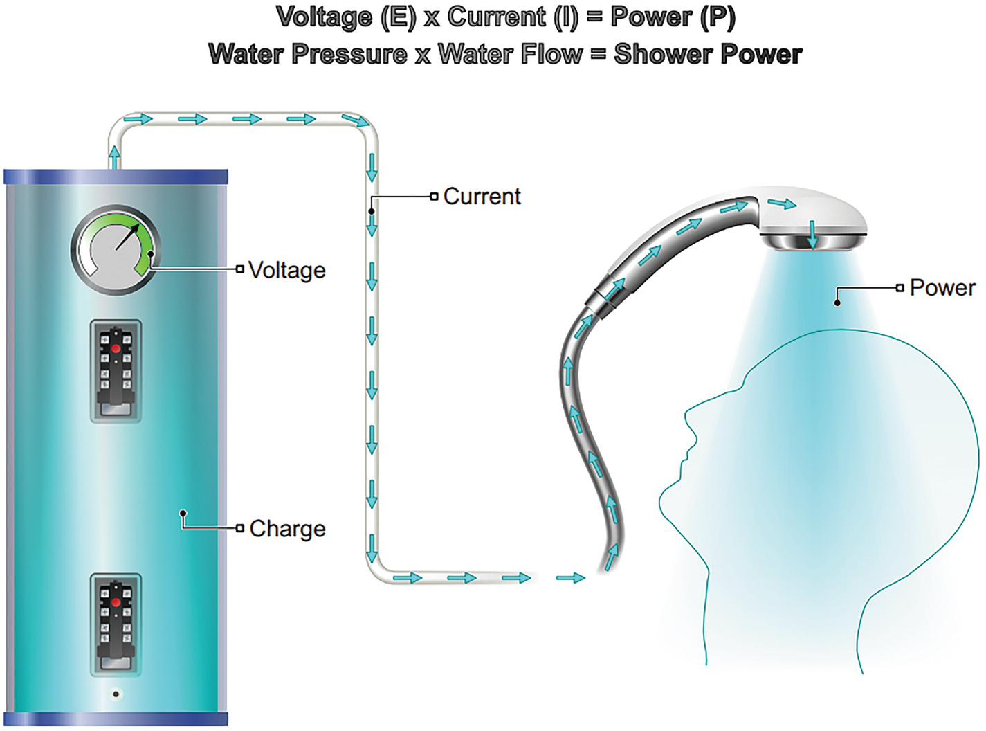
A diagram of the flow of current from a water heater to the head of a person. Equations of voltage, E multiplied by current I = power P and water pressure multiplied by water flow = shower power are exhibited above.
Joule’s Law and a Good Shower
Electricity describes the relationship illustrated by Joule’s Law. It is the phenomena in which voltage is applied to drive current, which happens when electrons are pushed to flow in the same direction. This happens at large scale in your local utility company that ships power to your home. But let’s face it, that's not really the interesting part to everyday consumers. The challenge is to figure out how to harness this current to do something useful. For that, we need a way to control the current we have created. All these flowing electrons (current) must be channeled through a material of some kind to make them useful as electricity. We need materials with conductivity.
Conductivity is a measure of how easily electric current can pass through a material. The key to performing useful work with electricity is to control conductivity – allowing current to flow in some cases and restricting it in others. That overhead light in your room would be much less useful if it was just on all the time or off all the time. Turning the current on and off is critical.
Conductors are materials with high conductivity (think metallic materials like copper and aluminum, which are the most common conductors used in electronics). Conductors have low electrical resistance, allowing electric current to flow through them easily. Resistance is measured in units called Ohms (Ω).
Insulators are materials with low conductivity (think materials like plastics or other polymers used to coat electrical wiring). Insulators have high electrical resistance, preventing or slowing the flow of electric current.
Semiconductors, as the name implies, are materials that sit between conductors and insulators – they can be both conductors and insulators. The key to the electronics revolution is the ability to control exactly when a semiconductor conducts, and when it insulates.

The diagram exhibits multicolored wires, which are protected by rubber inner and outer sheaths, made of a copper conductor within rubber insulation. A close-up shot of electrical wiring is on the right.
Electrical Wiring Left: Rubber Insulated Rubber Sheathed Red, Yellow, and Blue Three Core Round Cable (Jainsoncables, 2007) Right: “Twin and Earth” Electrical Cable, Commonly Used in the United Kingdom and Other Countries (Allistair1978, 2020)
By harnessing the properties of each of these types of materials, engineers can build elaborate systems that store and send information, solve complex problems, and perform all kinds of tasks that make modern technology possible.
Since the semiconductor is the key to this technology, let’s learn a little more about what a semiconductor is and how they are built.
Silicon – The Crucial Semiconductor

A photograph of purified silicon on a patterned floor. Its reflective surface is observed to feature many edges.
A Piece of Purified Silicon (Enricoros, 2007)
A Quick Semiconductor History
Before we dive deep into the details of the semiconductor design and manufacturing technology, it can be helpful to know just a little bit about its history and key inventors. Once scientists discovered the semiconductor properties of silicon, they were able to build simple transistors, which are basically switches that prevent current from moving forward or allow it to pass. By arranging transistors in intricate patterns, they realized they could selectively guide current along a path of their choosing and make it do some useful work along the way. For about a decade after the first transistor was invented in 1947, semiconductor design and manufacturing were slow, cumbersome, and costly.
Individual transistors and other components had to be manufactured independently, then fit together manually using “flywire” connections, which are basically metal wires connecting transistors to one another one at a time. A complete transistor circuit could literally fill an entire room. This was not going to be the basis for any kind of world-altering technological revolution.
All this changed in 1959, which can be officially observed as the beginning of the semiconductor revolution (doubtful we can get a national holiday and a day off out of it, but still worth noting). This was due to two key events. First, the invention of the integrated circuit by Jack Kilby at Texas Instruments, and Robert Noyce at Fairchild Semiconductor allowed hardware designers to fit a bunch of transistors together on a single chip (Nobel Media, 2000) (Kilby, 1964). Second, the invention of planar manufacturing by Jean Hoerni at Fairchild Semiconductor allowed chip companies to fabricate multitudes of components at the same time and on the same substrate (semiconductor base material, kind of like the foundation of a house but for computer chips) (Nobel Media, 2000) (Hoerni, 1962). Kilby received a Nobel Prize for Physics in 2000 for his work. Hoerni (deceased, 1924–1997) never received a Nobel Prize, but is widely recognized for his contributions. The importance of these core innovations – the integrated circuit (IC) and planar manufacturing process – cannot be overstated. They serve as the foundation of the design and manufacturing-based value chain that semiconductors and computers are built with to this day. We will cover each in detail in Chapters 3 and 4.
Semiconductor Value Chain – Our Roadmap
In trying to discuss a complex technical topic like semiconductors, it can be a real challenge to decide how exactly to tell the story. Should we start with “Once upon a time…” and proceed chronologically up to today? Should we start with the smallest elements like atoms and electrons, and work our way up to huge systems like computers and cars?
In Understanding Semiconductors, we’ve decided to tell the story just like a semiconductor company operates – from deciding what products to build, to designing and manufacturing them, to packaging and integrating them into the system.
We call this sequence the Semiconductor Value Chain, and it will serve as our roadmap for our entire journey. We’ll go on a few detours to discuss some fundamentals and a couple of special topics, but for the most part, everything that follows in this book can be tied back to a part of this core sequence and can serve as a mental foundation on which to build your understanding of the industry as a whole.
- 1.
Customer need and market demand: First, the need for a “system” or product must be established. A new system could be anything from a rocket ship control panel to the next iPhone. What is important here is that there is a market need – without a customer, why build a new system in the first place? But remember, customers may not always tell you what they need. Recall the classic quote from Henry Ford, “If I had asked people what they wanted, they would have said faster horses.”
- 2.
Chip design: Second, a firm must consider a product and design a chip that will fit that product accordingly. This design process is broken down into front- and back-end design. To make sure this is clear, here’s what happens at each step:
Front-end design: System requirements are gathered, and a detailed schematic is developed to create a design concept. This design concept is tested and verified before moving to back-end design.
Back-end design: A detailed list of instructions, called a netlist, is converted into a physical layout, which can then be tested and validated before being sent to a factory called a semiconductor fabrication plant, or fab, for manufacturing.
- 3.
Fabrication and manufacturing: Third, a design must be manufactured at a wafer fab. In this step of the process, numerous integrated circuits, also known as die or IC’s, are printed onto a sheet of silicon called a wafer through a process called photolithography.
- 4.
Packaging and assembly: Fourth, once the die have been cut apart from one another, they are individually packaged in plastic or ceramic packages called IC packaging in a process called assembly. These package-die assemblies are tested one last time before being sent to end systems or product companies.
- 5.
System integration: Once the system or product company has received the final die-package assembly, they can solder it onto a larger circuit board or substrate with other components or ICs and integrate it into the end, consumer-ready product.
- 6.
Product delivery: The product is shipped to customers, where it is ready to be used.

The diagram exhibits six illustrated steps namely customer need and market demand, chip design, fabrication and manufacturing, I C packaging and assembly, system integration, and product delivery.
Semiconductor Value Chain
For the most part, semiconductor companies concentrate on Steps 2–5. And, in fact, some companies (called ‘fabless’ companies) really only do step 2. They design the chip, and then outsource most of the other steps. Companies start by forecasting market demand or collecting orders from downstream device companies and focus their energy on building chips that can satisfy the needs of their customers. Since the industry’s inception in the 1940s, this value chain has remained, conceptually, relatively stable. At the same time, however, the organization and business strategies of how each step is done have been incredibly dynamic, driven by innovative companies competing to provide the best performing chips and highest quality products. We will use this value chain to guide our discussion of key sub-processes and anchor our understanding of each step to the bigger picture.
Performance, Power, Area, and Cost (PPAC)
For semiconductor companies focused on the design, manufacturing, assembly, and integration portions of the value chain (steps 2, 3, 4, and 5), the goal is to achieve the Highest Performance, using the Lowest Power and the Smallest Area possible. These three key design metrics are typically measured in clock frequency (Hz), watts, and nanometers (nm), respectively. Each semiconductor design may trade off one of these for the others, depending on the application. For example, a team designing a chip for a server in a data center with plenty of space and an industrial grade power source may focus on performance, while not caring as much about size or power. A team designing a chip for a battery-powered cell phone, however, may be concerned more about power and size than performance. For any given application, the goal is to optimize a chip design along these three constraints at the Lowest Cost and in the Shortest Time frame possible. We can better picture how these factors relate to one another in Figure 1-14.
Each chip must balance PPAC constraints to provide an optimal solution. Design teams must keep in mind the problem they are trying to solve and the application the circuit they are building is meant to address. For example, plugged-in devices like desktop computers may not have to optimize for power consumption as much as battery-powered laptops. Laptops, in turn, may have greater flexibility on area than smaller, hand-held devices like cell phones. It is important not to forget time as a key constraint as well – it may be worth lower performance if you can cut your design cycle short and beat your competitors to market. There are virtually limitless applications of circuits, all with unique performance, power, area, cost, and time constraints – the important thing is to understand the trade-offs.

A diagram exhibits the interconnections among power, performance, area, and cost via a three-dimensional triangle. Each has a bulleted list of its own aspects.
Power vs. Performance vs. Area vs. Cost (PPAC)
Who Uses Semiconductors?
SIA Framework – End-Use Applications
 A table has 2 columns and 6 rows. The columns are labeled market and specific applications, while the leftmost rows are labeled consumer, automotive, computing, industrial, communications, and government. A table has 2 columns and 6 rows. The columns are labeled market and specific applications, while the leftmost rows are labeled consumer, automotive, computing, industrial, communications, and government. |

A pie chart has 6 slices. Computing holds the biggest slice with 32% followed by communications with 31%, industrial and consumer with 12% each, automotive with 11%, and government with 1%.
2020 Semiconductor Market by End Use Application (SIA and WSTS) Power vs. Performance vs. Area vs. Cost (PPAC)
Each of these applications has different PPAC requirements and drivers based on their unique purpose, which impacts each stage of the design, manufacturing, and assembly processes.
Summary
In this chapter, we examined how electricity and conductivity work together to make semiconductor technology possible. We discovered what semiconductors are, what they do, and why silicon is the most useful one. We introduced the Semiconductor Value Chain that converts ideas and raw materials into chips and finished products. Finally, we reviewed the key PPAC parameters that shape how chips are optimized for their intended purpose and what those real-world applications actually are.
The ideal chip is high performance, requires low power, and takes up little space. Accomplishing all three would be ideal, but cost and time force us to make tough choices. Each step of the value chain is essential to get a chip from concept to customer – at every stage, companies fight for profits and market share by balancing these factors more effectively than their competitors.
Your Personal SAT (Semiconductor Awareness Test)
- 1.
Define electricity and conductivity. How do they relate to current and charge?
- 2.
What is the most important semiconductor and why?
- 3.
Which two inventions are responsible for the modern semiconductor industry? Why were these innovations so important?
- 4.
After fabrication and manufacturing, what step in the semiconductor value chain is necessary before system integration? Can you name all six?
- 5.
What does PPAC stand for? Can you name which key design factor is missing?