
Chapter 8
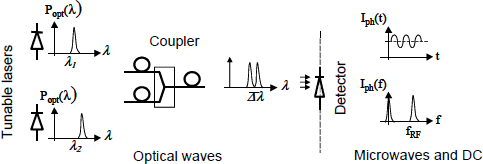
Simulation and Measurement of Microwave Photonic Links
8.1. State of the art and context
8.1.1. Objective
The objective of this chapter is to present the possibilities offered by a purely microwave simulation software to model and characterize an optical-microwave link. Actually, the chosen software is not specifically designed to simulate optical components or model electro-optic transducers. A major benefit of this tool is the possibility to define large signal or nonlinear and noise models. The simulation allows the characterization of a microwave optical link, and provides information regarding the evolution of gain, noise values, and nonlinearities of a photonic link as a function of various parameters, such as frequency or optical attenuation. A strong asset is the study of radio-over-fiber (RoF) systems including the optical tunnel but also microwave components before and after the optical link. It is also possible to study the effects due to temperature variations on the behavior of different components in the models. However, these effects will not be presented in this chapter.
8.1.2. Choice of simulation software
It is very useful to be able to quantify the characteristics of a microwave optical link with a simulation tool before its realization.
Certain software dedicated to optical solutions exist, such as IPSIS COMSIS [COM], or VPI. For this type of software, it is not easy to integrate purely microwave components in the link with their own characteristics, as well as generating digital signals to transmit on the optical fiber.
The approach in this study focuses on a purely electrical system circuit simulation software, ADS. The Agilent ADS system is an electrical circuit design software allowing co-simulation. This software accounts for noise characteristics, and nonlinearities of microwave monolithic integrated circuits situated before or after the optical link.
The benefit of using an electrical system simulation software is to simulate microwave optical links transporting, for instance, orthogonal frequency division multiplexing (OFDM) complex digital signals [BEN 09] or pulse coding, such as multiband on-off keying (MB-OOK) [LEG 09; PAQ 04], and to use real signals for data inputting. It is then possible to quantify the impact of the optical transmission part on the quality of the link, independently of that of the purely electrical circuits. The two impact types can thus be cumulated in order to evaluate the more influential of the two, which is impossible with current software dedicated to optical systems.
In this environment, the electrical signal amplitude and phase information is available. In Chapters 2, 3, and 4, the electrical models of each link component were presented. After having defined input and output impedance matching for each model, the optomicrowave S-parameter notion was defined in Chapter 5. These notions will be used for the simulation.
8.1.3. Different ADS simulation techniques
Different digital simulation techniques allow the optimization of computation times, or studied systems inputs/outputs to be predefined according to strong or weak system nonlinearity.
Two principal simulation types exist:
– linear simulations, which operate in the frequency domain by considering each component by its frequency transfer function. The signals are developed in a Fourier series;
– nonlinear simulations, which operate in time domains and allow component nonlinearity accountability. A Fourier transform allows the determination of the spectral response of the circuit.
In the first type, the signals have low amplitude and the components operate at a fixed biasing point. In the second type, the signals have high amplitude and the component biasing point can vary.
Linear simulations are accessible via AC simulators, and nonlinear simulations through DC, harmonic balance (HB), time-domain, and envelope simulators.
Static simulation, with the help of a DC simulation technique, allows the computation of DC voltages and currents of a mounting, as well as plotting the static characteristics of the components.
The linear simulation of frequency requires an AC small signal simulation technique. It allows a frequency analysis and determines the currents and voltages at diverse circuit nodes, the transfer parameters computation (voltage and current gains, transimpedance and transadmittance), and linear noise computation.
The “S-parameters” technique computes electrical S, Y, Z linear parameters and the linear noise of equivalent circuits allowing a circuit analysis performance as a function of matching.
Frequency nonlinear simulation or fixed frequency with a variable power is available with the help of a HB technique. This continuous wave (CW) mode frequency analysis allows the simulation of distortions due to nonlinear effects.
Multi-tone excitement computes intermodulation products. Linear circuit analysis is performed in the frequency domain, whereas nonlinear circuit analysis is performed in time-domain simulation; combination of the two analyses gives the solution.
Time-domain simulation enables circuit transient analysis and provides the response to a complex excitation. It can be very long in the case of strong circuit nonlinearity.
Envelope simulation allows the displacement of the analysis from low frequency towards a higher central frequency by limiting the number of sampled points while respecting the Shannon criteria. This simulation type analyses microwave signals modulated by complex signals, when the frequency ratios between modulation and carrier are too large to correctly visualize the time-domain simulation signal.
The “Ptolemy” simulation system analyses base band signals propagating on complex communication systems and allows the visualization of the influence of the latter on the propagation of these signals. In system simulations, the signal containing the base band information is transposed at RF (fRF) along the length of the transmit/receive chain. Each of the circuits constituting the system is assimilated to a black box containing the principal circuit characteristics and performances in terms of bandwidth, gain, matching, compression at 1 dB, intermodulation products, etc. Thus the influence of RF circuits on the signals is generically computed. In order to very precisely account for a circuit performance in a given technology (e.g. MMIC circuit designed with the component library of an MMIC foundry), during system simulation, the Ptolemy simulator can call on one or several simulator circuits (HB, AC, S-parameters, time-domain) to more precisely simulate a circuit response. A co-simulation is thus performed, Ptolemy, recovering circuit simulated digital data rather than generic data. This procedure allows the very precise evaluation of real microwave circuits on digital signals constituting the flux of data to transmit across the system.
8.2. Microwave optical link models
In the remainder of this chapter, the simulations of different microwave optical link components are presented, as well as the simulation results of this direct link modulation.
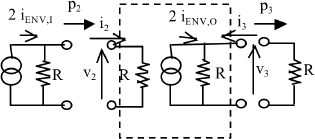
8.2.1. Two-port network approach
As explained in Chapter 5, each of these link components are described as a two-port (quadrupole) network with two poles earthed.
As this link uses optical and microwave notions, it is chosen to define the link optomicrowave transducers using purely microwave modeling. Also it is not the optical power, but rather the envelope of the detected optical power that is represented by current iENV. This current corresponds to that detected by a perfect photodetector lit by the transmitted optical power (Figures 5.1 and 5.2).
In Chapter 5, the gain plots are obtained for an optomicrowave link with simplified and linear models as indicated in Figure 5.3. For example, the laser electrical model has an internal resistance, rL, and a current-controlled current source loaded by a 50 Ω resistance modeling the optical side-matching.
In this chapter, nonlinear electrical models are used. They are more sophisticated than those defined in the theoretical approach presented in Chapter 5. This permits the precise accounting of the steady state and dynamic responses of link components. Integration of nonlinear effects in the link is facilitated by the ADS circuit-system simulation tool.
8.2.2. Electro-optic transducer: the laser
The laser modeled in this chapter is a wideband DFB laser. The electrical diagram relying on the Tucker model [TUC 83] models the laser. It was presented in Figure 2.21 of Chapter 2 and is recalled in Figure 8.1.
Figure 8.1. Laser equivalent diagram for simulation
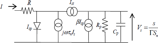
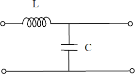
The parasitic elements due to the biasing circuit are generally accounted for at the laser diagram input. The capacitive and inductive elements values are defined by microwave measurements of the laser to model.
An example of a parasitic circuit is given in Figure 8.1.
The equivalent two-port network adjustment parameters are the physical parameters of the laser depending on the electrical policy of the foundry and so are difficult to access. However, the available information is: steady state response and RIN measurements for different biasing currents.
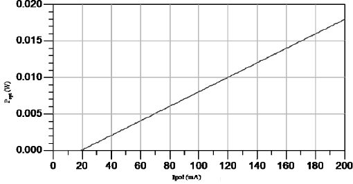
The useful steady state characteristics of the modeled DFB laser are:
− the threshold current is equal to 20 mA;
− the laser diode sensitivity is 0.1 W/A;
− the optical wavelength is 1,550 nm.
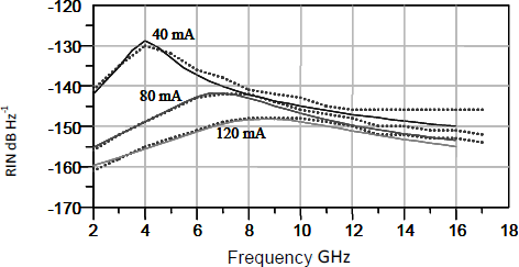
The dynamic response can be directly extracted from RIN measurements, visualized in Figure 2.26. As a result, the amplified spontaneous emission is a white noise, so the RIN measurements constitute the laser intrinsic dynamic signature. Contrary to the dynamic laser S21 parameters response, the access circuits do not influence the intrinsic dynamic response of the studied component for a white noise. However, to obtain the laser dynamic response from S21 parameter, it is first necessary to extract the access circuits effects.
From steady state and intrinsic dynamic response characteristics known from the laser, a set of complete system parameters is obtained. The resolution of the carriers and photon rate equations allows the extraction of a set of physical parameters for the laser electrical model under ADS. The useful components are the carrier and photon lifetimes, the differential gain factor, spontaneous emission fraction, and the gain compression factor.
After having modified the adjustment parameters in the electrical equivalent circuit, the steady state and RIN responses are presented hereafter.
The model adjustment parameters are the physical parameters of the laser. The physical parameter values were defined by optimizing in the steady state response and the RIN.
Figure 8.3 shows the validation of the laser electrical model for steady state behavior. As a result, the values of threshold current (20 mA) and laser sensitivity (0.1 W/A) obtained by simulation, correspond to measured characteristic laser values.
Figure 8.3. Simulation of DFB laser steady state response
In Figure 8.4, the RIN simulation results are compared to RIN measurements. The RIN simulation technique was presented in section 2.1.10.2; this will be recalled in section 8.4.1. A good agreement between simulation results and RIN noise measurements, as a function of frequency, allows the validation of the dynamic laser electrical model.
As the simulation model has been validated by dynamic measurements, it is now possible to simulate the response of the laser S-parameters [BDE 06; PAS 02].
Figure 8.4. Comparison of measured (…) DFB laser RIN and simulated (—) plots
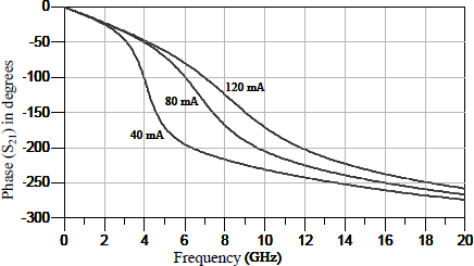
The laser S21 parameters simulations are presented below, for biasing current values of 40, 80, and 120 mA. The S21 parameter has a complex value; therefore Figures 8.5 and 8.6, respectively, represent the amplitude and phase of the DFB laser model S21 parameter.
Figure 8.5. Modulus of simulated DFB laser S21 parameter a function of frequency
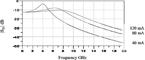
Because the laser gain is more or less powerfully influenced by the physical phenomenon of relaxation, a useful asset of this microwave circuit simulation tool is it accounts for the influence of the relaxation oscillation frequency on the laser model as a function of biasing current and frequency.
An additional interest to the modeling approach of this microwave optical link is the knowledge of the transmitted microwave signal phase evolution as a function of microwave modulation frequency.
Figure 8.6 presents the curve of the microwave signal phase as a function of laser biasing current and microwave modulation frequency.
Figure 8.6. Phase of DFB laser simulated S21 parameter as a function of frequency
8.2.3. Transmission guiding: the optical fiber
The optical fiber is modeled by an electrical two-port network of which input and output are matched to 50 Ω. This matching reflects the hypothesis that there is no input and output optical reflection from the optical fiber. This hypothesis does not exactly reflect the reality but is realistic for an initial approach. The physical phenomena accounted for in the optical fiber model are the attenuation and chromatic dispersion.
The attenuation is characterized by the attenuation coefficient α, expressed in decibels per kilometer. The attenuation on an optical fiber of length L is written:
LOF can also include fixed fiber-photodiode and laser-fiber optical coupling losses. The chromatic dispersion physical phenomenon was explained in sections 3.1.3 and 6.1.2.
During the signal transmission on the optical carrier, the microwave signal undergoes a phase difference. The mathematical expression of the electric field allowing the formalization of the impact of different effects was presented in sections 3.1.4 and 6.1.3. After photodetection, the current expression, explained in the same sections by equations [3.13] and [6.14], is recalled:
where Rpd is the responsivity of the photodiode.
The optical fiber transfer function for an input microwave signal accounts for the φ1 phase difference proportional to the microwave angular frequency in the following manner:
where:
tg: is the group time per unit length;
L: the optical fiber length;
vg: the group velocity in the fiber.
A microwave signal of frequency fRF modulating in double sideband an optical carrier, after transmission over an optical fiber of length L, is weighted at the detection by the cos φ2 coefficient expressed in the following form:
with:
λ0: optical wavelength;
D: chromatic dispersion factor.
The cos φ2 term cancels the detected signal for particular transmission lengths L, as a function of modulation frequency.
At a 1.55 μm optical wavelength, the linear attenuation α is taken to be equal to 0.2 dB/km and the chromatic dispersion factor D is equal to 17 ps/(km.nm) for a SMF standard optical fiber (G.652).
In Table 8.1 transmission lengths for which the detected signals cancel are presented.
Table 8.1. Distances defining the first transmission zeros after detection as a function of the modulation frequency
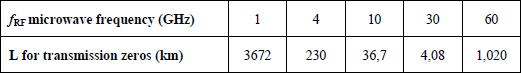
The chromatic dispersion phenomenon is characterized by a photodetected signal cancellation for optical fiber lengths, which depends, amongst other things, on the transmitted microwave frequency.
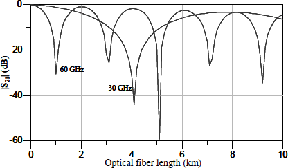
Figure 8.7 presents the simulated optical fiber gain plots for a 1.55 ìm wavelength for two different microwave frequency values.
The first signal cancellation detected at 60 GHz appears for a transmission length of approximately 1 km; however, for a microwave signal of 30 GHz, the transmission length possible without cancellation is increased and is equal to approximately 4 km. These values extracted from the simulation results are identical to those presented in Table 8.1.
The electrical two-port network from the optical fiber model has a current-controlled current source equal to the optical power envelope entering the optical fiber.
Figure 8.7. Microwave optical gain variation as a function of optical fiber length for 30 and 60 GHz modulation frequencies
The envelope current link between input and output is defined as a function of optical loss by:
It is important to recall that the LOF value of optical loss in decibels indicates electrical losses equal to 2.LOF in the power assessment of the microwave optical link.
As a result, the optical power transmitted in the optical fiber is proportional to the laser control current, as well as to the photodetected current, while the microwave power is proportional to these currents squared.
From the chosen optical microwave approach, which is presented in the figure below, the electrical two-port network modeling the optical fiber is input and output matched. Thus, the following hypotheses are valid: S11 = 0, and S22 = 0, interpreted as no reflection at the input and output of the fiber. In this case, it can be written:
It is also assumed: S12 = 0. The optical link simulated has no return towards the input.
The optical fiber parameter S21 phase variation corresponds to the φ1 physical parameter. For a 1 km length optical fiber, with a 17 ps/(km.nm) dispersion, the microwave phase variation is equal to 1.8° for a 1 kHz modulation frequency variation, as illustrated in Figure 8.9.
Figure 8.9. 1 km optical fiber electrical phase variation
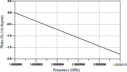
With the help of Figure 8.9, it is thus possible to express the phase variation per kilometer transmitted on an optical fiber, and frequency deviation relative to the microwave carrier per kHz.
8.2.4. The optoelectric transducer: the photodiode
The photodetector converts the optical power fluctuations lighting the photodetection window into current fluctuations. The operating principles of photodetectors are described in Chapter 4.
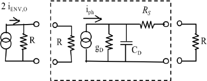
The electrical equivalent circuit for the photodiode developed using ADS has a current source controlled by a parameter proportional to the incident optical power, a capacitance corresponding to the diode transition capacitance, due to the depleted zone, and a resistance, corresponding to the inversed biased junction dynamic resistance. Additionally, a resistance RS is presented to model the contact resistance effect.
The photodiode equivalent two-port network input signal corresponds to the optical power envelope. The incident optical power envelope is thus represented in the model by the resulting current following optical power detection by a perfect photodiode. The two-port network output signal is an electrical signal photodetected by the photodiode.
The photodetector electrical model is given in Figure 8.10.
Figure 8.10. Photodiode linear model
This model is usually completed by a parasitic elements circuit placed at the photodiode output whose values are extracted from microwave measurements performed on the photodetector. A parasitic circuit example is defined in Figure 8.11.
Figure 8.11. Photodiode output parasitic elements example
It is possible to define a model taking into account the transit time, a physical phenomenon explained in section 4.2.3.
A 50 Ω resistance R is introduced at the photodiode equivalent two-port network input to model an optical reflection absence at the photodiode input. Thus, the photodiode electrical model input is impedance matched to the output of the equivalent electrical circuit of the optical fiber.
A current source with a parallel internal resistance taken as R (50 Ω) is defined. The intensity produced by the optical fiber current source is defined so the current dissipating in resistance R at the photodiode model input is equal to iENV,O.
The photodiode is characterized by its responsivity Rpd in A/W in the following manner according to equations [5.8] and [5.11]:
[8.8] ![]()
The controlled-current current source is defined by equation [8.8]. The photoelectric current iph is then proportional to the optical power envelope popt,O, iENV,O, defined in section 5.1.1.
It is important to note that output currents are often confused with the photoelectric current iph in different models in the literature. With this convention, the effect of the circuit composed of parallel resistance and capacitance, and the series resistance, is neglected and the study is reduced to relatively low frequencies. In this section we depart from this hypothesis and the low-pass circuit is introduced.
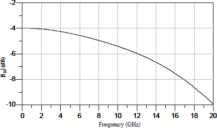
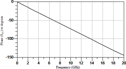
The modeled photodiode has a bandwidth greater than 12 GHz, a responsivity of 0.8 A/W, and a low-pass frequency response.
To respect these constraints, the modeling parameters and interference components are specified in Table 8.2.
Table 8.2. Element values of the photodiode model used with ADS
The optomicrowave gain of this photodiode is represented in Figure 8.12.
Figure 8.12. Simulated dynamic response amplitude of the photodetector loaded by 50 Ω
The variation of the photodetected microwave signal phase, as a function of microwave modulation frequency is presented in Figure 8.13.
Figure 8.13. Simulated dynamic response in phase for the photodetector
8.3. Nonlinearity effects in the link
8.3.1. Nonlinearity sources
8.3.1.1. Laser nonlinearity
Several nonlinearity sources are present in the laser.
First of all, the chosen method for laser modeling relies on continuity equations, presented in section 2.1.10, and recalled below:
[8.9] ![]()
[8.10] ![]()
with N and P the number of carriers and photons in the active layer, NT the number of carriers at transparency.
Dynamically, parameters ![]() and
and ![]() vary, the N.P product, present in the two continuity equations [8.9] and [8.10], implicates nonlinear effects introduced by the laser. Additionally, a compression factor, ε, introduces an additional nonlinearity.
vary, the N.P product, present in the two continuity equations [8.9] and [8.10], implicates nonlinear effects introduced by the laser. Additionally, a compression factor, ε, introduces an additional nonlinearity.
The laser steady-state characteristic is nonlinear. On the one hand, the laser steady-state response saturates for strong biasing currents. For DFB lasers, this effect is insignificant, as these biasing points are not attained. However, the impact of this effect must be studied when it is a VCSEL as the plot of the optical power steady-state response as a function of biasing current rapidly saturates for this laser type [LEG 09]. On the other hand, the effect of an “optical power-biasing current” steady-state response bend presence causes nonlinearity. This bend appears as the laser control current becomes close to the threshold current.
8.3.1.2. Photodiode nonlinearity
The current-controlled current source is defined by the linear equation [8.8].
The photodiodes present a nonlinear response as the incident optical power exceeds a certain optical power level. To introduce this nonlinearity in the model, the linear equation [8.8] is replaced by the following:
The ki factors depend on the photodiode output microwave power relative to the different spectral lines (fundamental and harmonic).
8.3.2. 1 dB compression point and first-order dynamic of the link
The nonlinearity previously presented is characterized from a link point of view by the compression at 1 dB. The definition of this particular point was presented in section 5.8.1.
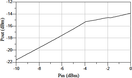
The ADS electrical circuit simulation software takes into account component nonlinearity. Thus, it is possible to visualize the electrical power level at the photodiode output as a function of the electrical power at the link input, for a defined modulation frequency.
The plot of Figure 8.14 presents the curve of the output electrical power as a function of the input power for a 3 GHz modulation frequency, the biasing current being equal to 40 mA. The break of this line actually comes from the link nonlinearity as the input power increase pace is defined at 0.1 dB for the simulation. For this configuration, the 1 dB compression point corresponds to a −2 dBm input power.
Figure 8.14. Simulated output electrical power of the link as a function of the input electrical power
The dynamic response of a link is defined in section 5.9. The link output noise power level being equal to −144 dBm/Hz, the first-order link dynamic, relative to the point of 1 dB compression, is equal to 129 dB.Hz for the configuration presented in Figure 8.14.
8.3.3. Third-order intermodulation and third-order interference-free dynamic range of the link
A parameter allowing the quantification of the impact of nonlinearity on the link is the notion of third-order intermodulation, which is presented in section 5.8.3. In Figure 8.15 the electrical power at the link output is plotted. Fundamental lines at 3 GHz and 3.1 GHz, which superimpose upon each other, form the third-order intermodulation product (IM3) corresponding to a line at a frequency of 2.9 or 3.2 GHz. The noise power as a function of input electrical power is also shown. These plots are for a biasing current of 40 mA.
Figure 8.15. Simulated third-order intermodulation and output noise power
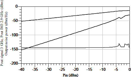
The third-order interception point (IP3) and the third-order interference-free dynamic range (D3), explained in section 5.10, can be directly taken from Figure 8.15, knowing that the link output noise power is equal to — 144 dBm/Hz. For two input modulation frequencies of 3 and 3.1 GHz, for a 40 mA biasing laser current, the third-order interception point is equal to 10.3 dBm for the input power and −1.3 dBm for the output power, the link dynamic range is equal to 95.5 dB.Hz2/3. The 1 dB compression point and the third-order interception point change with the laser biasing current and the fRF frequency signal. A laser biasing current increase induces an increase of 1 dB compression point defined at the input and the third-order compression point, in so far as the fRF frequency signal is far from the laser relaxation oscillation frequency.
8.4. Link noise modelling
8.4.1. Noise in the laser
The noise sources considered in the laser are partly thermal noises due to the source resistance and partly due to the laser RIN.
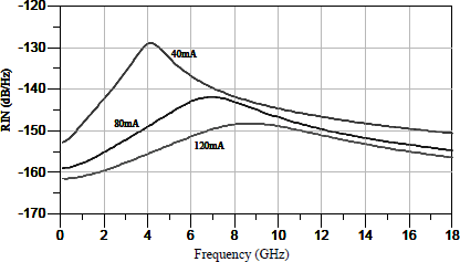
To model the thermal noise using ADS software, the source resistance is defined as noisy. As for the RIN modeling, current noise sources characterized by Langevin forces are added in continuity equations as presented in section 2.1.10.2. Thus, the RIN simulations plots, for different biasing currents, are presented in Figure 8.16.
Figure 8.16. RIN noise simulation for three biasing currents of 40, 80, and 120 mA
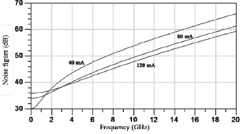
As the laser diode is modeled by an electrical two-port, it is possible to define the laser noise figure. The modeled laser noise figure is plotted as a function of signal modulation frequency for direct modulation case in Figure 8.17.
Figure 8.17. Development of the value of laser noise figure as a function of modulation frequency for three biasing currents
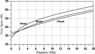
The benefit of laser modeling and simulation tools is the plotting of the laser noise figure evolution as a function of the frequency for different biasing currents. These different simulations show the impact of each parameter.
8.4.2. The optical fiber
The assumed hypothesis is that the optical fiber produced no noise. Also, the optical fiber noise figure, no matter the transmission length, is considered equal to 0 dB.
8.4.3. Noise in the photodiode
The different noise sources from the photodiode are shot noise due to the photodetected average current, shot noise due to obscurity current, and thermal noise due to photodiode conductance gD. Shot noises are modeled by two current noise sources. The conductance gD is considered noisy, the thermal noise is generated by the ADS software.
As one of the noise sources (shot noise) depends on the detected current, the photodiode noise figure depends on the value of the input current modeling the incident average optical power envelope. The photodiode noise figure is represented in Figure 8.18.
Figure 8.18. Photodiode noise figure for a DC current of 12.44 mA at the input of the photodiode
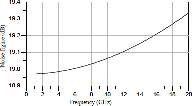
Photodiode noise figure depends on the DC optical power level present at the input. The higher this level, the more noise figure is produced. To illustrate this variation, the modeled photodiode noise for a 3 GHz microwave modulation frequency and for DC input currents varying from 5 to 15 mA, is between 15.1 and 19.8 dB.
8.4.4. Direct modulation link noise figure
The direct modulation link is modeled using ADS; this simulation tool supplies a noise figure for the total link noise. In Figure 8.19, noise figure is plotted as a function of the modulation frequency for a 100 m optical fiber for three different laser biasing currents.
Figure 8.19. Simulated values for link noise figure for three biasing currents
Each direct modulation link component is modeled by an electrical equivalent circuit; it is possible to have access to the optomicrowave gain and to the noise figures for each link element. These data allow the calculation of total link noise figure by applying the Friis formula to the optomicrowave link, as undertaken for purely microwave channels. The Friis formula is recalled below:
It is then possible to evaluate the total link noise factor from the values of component gain and noise, expressed in linear mode, from the link components.
In the following table, a excellent convergence is observed between the noise figures for total link simulated using ADS and those obtained by calculation with the help of the Friis formula for four optical fiber lengths (0.1, 1, 30, and 100 km) and for a modulation microwave frequency of 3 GHz.
Table 8.3. Summary of the noise figures for three biasing currents, four optical fiber lengths, and a fRF modulation frequency at 3 GHz
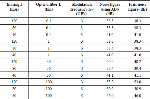
The good agreement between the noise figure for optical-microwave link obtained by two different methods confirm the assumption the optical fiber does not add any additional noise.
8.4.5. Noise power at the receiver
To have precise knowledge of signal quality in comparison to the noise, the noise figure is a relevant point. Another approach is to look at receiver noise power. While the noise figure depends on the link source impedance, the output noise power depends on the load resistance at the receiver side.
The expression connecting output noise power to noise factor is the following:
[8.13] ![]()
Each component of equation [8.13] is expressed in a linear value. The input incident noise power is thermal and equal to:
with:
k: Boltzmann constant (k = 1.38×10⁻²³ J/K);
T: temperature in K;
B: microwave bandwidth in Hz.
The expressions of corresponding transducer gain and noise factor for a direct modulation optomicrowave link with a simplified laser model, are presented in Chapter 5. They are recalled below:
The equation of the average photodetected current is expressed in the following form:
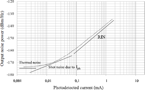
Also, it should be noted that noise power depends on three terms. The first relative to RIN is weighted by the square of the photodetected current; the second, shot noise due to photodetected current linearly varies with this; and the third, corresponds to obscurity current shot noise and thermal noise associated with the photodiode charge which is independent of the photodetected current.
The simulations of photodetector output noise power are plotted as a function of photodetected current Iph, for different biasing currents in Figure 8.20.
Figure 8.20. Simulated output noise power at 3 GHz
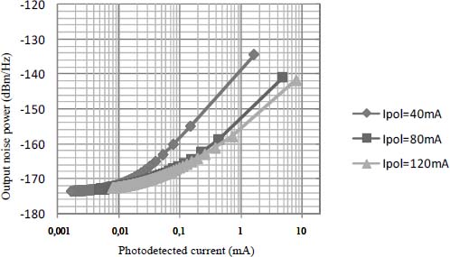
The noise decreases as a function of the biasing current at 3 GHz can be explained by reviewing the plots of Figure 8.16. In the used laser model, the RIN level depends on the biasing current and the modulation RF frequency. Contrary to the curves of Figure 5.30 for which the RIN is constant.
The slopes are seen in Figure 8.21. They reflect the dominant noise level as a function of the photodetected current. The influence of the biasing current exists for low optical attenuations for which the RIN impact is predominant.
The optomicrowave link output noise power measurement provides the noise figure when the link gain is known [BIL 10].
In order that the output noise power only comes from the optical-microwave link, care must be taken to remove the noise coming from the load resistance of the measuring equipment. Thus, it is necessary to measure the noise power behind a low-noise amplifier, which in this case allows noise amplification after the link output. This renders the thermal noise brought back by the measuring equipment load resistance negligible in comparison to the link noise power that needs to be measured.
Figure 8.21. Highlights of the three slopes: simulated noise power plot for Ipol = 40 mA
The measurement of the low-noise amplifier output noise power provides information regarding the noise of the non-electrically amplified microwave optical link at the photodiode output when the optical microwave link gain without an amplifier stage and the noise figure value for the low-noise amplifier are known.
8.5. Other types of modulation of signals transmitted on an optical fiber
8.5.1. Ultra-wideband signal modulation
The benefit of using microwave system simulation software is the ability to integrate other non-sinusoidal source types, e.g. an ultra-wideband (UWB) or pulse signal source. In this case, the time-domain simulation technique is the most useful. It is, therefore, possible to study the impact of UWB signal propagation in an optical tunnel on the quality of this signal and to quantify the degradation.
Wireless and optical fiber hybrid radio links transporting UWB signals are a recent subjects. Because of the need to emit power limited UWB radio signals, radio communication distances are short, typically lower than 100 m. To increase the scope of these UWB radio signals, this signal type can be distributed on optical fibers [LEG 09; YAO 09] to attain theoretical data rates of 10 Gb/s.
In the framework of the ANR BILBAO project [LEG 09] (Bornes d’Infrastructures Large Bande à Accès Optique), the propagation of an UWB signal modulated by a MB-OOK technique, in an optical tunnel was studied. Part of this study is presented in this section. The modulation technique itself (MB-OOK) is not necessarily a promising solution but it is a good example of the possibilities of simulation with pulse signals. The MB-OOK modulated UWB transmit/receive architecture operational scheme is defined in Figure 8.38. A complete MB-OOK architecture simulation was performed, by applying a variable amplitude monocycle pulse signal at the input. All the functional units of this architecture were modeled using ADS software.
Figure 8.23 represents four time-domain signals taken from the receiving channel, at each of the four elliptical filter outputs for a “0101” transmitted signal.
Figure 8.23. Output time signal of each of four reception filter corresponding to a “0101” signal
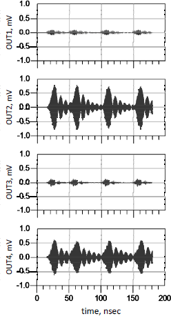
Figure 8.24 represents the four frequency signals taken from the receiving channel, at each of the four elliptical filter outputs for a “0101” transmitted signal.
Simulations enable the estimation of the minimum level of the optical link input electrical pulse based on electrical equivalent circuit of a low-cost VCSEL, of the optical fiber and photodiode. By considering the worst case scenario in terms of link output noise and to avoid that the minimum peak amplitude of the output optical link is drowned in the noise, the minimum peak amplitude of the pulse modulating the laser at the optical link input was estimated to a value in the order of 1 mV.
Figure 8.24. Frequency signal simulation at receiving filter output
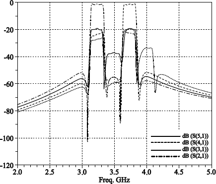
The optical link input pulse maximum level was evaluated with the help of simulations, given the nonlinearities introduced by the optical link when the input power levels become too high. At this effect, two configurations were studied: the first represents a realistic MB-OOK link with elliptical filters with 18 dB rejections and the second configuration is an ideal MB-OOK with 100 dB rejections for simulated filters.
Figures 8.25 and 8.26 present the line of the three adjacent channels output powers, permitting “010” bits transmission, as a function of input power. Plot P1 represents the output power of the channel transmitting bit “1”, while power plot P2-P3 represents the channels transmitting bit “0”.
For the configuration using 18 dB rejection filters, the three output signals taken from four adjacent channels develop in a linear and parallel manner for input signals lower than 80 dBm. It must be recalled that 80 dBm is very far from a realistic value. A gap of approximately 20 dB exists between the fundamental signal and the two signals in each of the adjacent channels. Above this, the signals saturate and stay parallel keeping the same 20 dB gap. This constant gap corresponds to the 18 dB rejection filters and not to an intermodulation phenomenon. As a result, when the pulse is filtered across each of the filters, the rejection results the attenuation of the signal corresponding to adjacent channels by at least 20 dB. Thus if a channel transmits a “1” level, the adjacent channels recover the attenuated signal of at least 20 dB due to the filter effect.
Figure 8.25. Evolution of the MB-OOK architecture simulated output power for the three adjacent channels transmitting “010” bits as a function of input power (18 dB rejection filters)
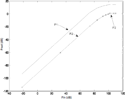
For the second configuration, a linear evolution parallel to the signals for input powers lower than 80 dBm is observed. Nonlinearity, therefore, occur for an excessively high input power, which is again not realistic. The gap between the fundamental signal and the two signals in the adjacent channels is 45 dB, corresponding to the minimum rejection due to the slope of the filter in this channel. Above an input power of 80 dBm, saturation of the fundamental signal occurs and the two intermodulation signals appear: the response is no longer linear. As the input power increases, the gap between the fundamental signal and intermodulation signal is reduced. The gap goes from 45 to 20 dB.
Figure 8.26. Line of the MB-OOK architecture simulated output powers for three adjacent channels transmitting “010” bits as a function of input power (100 dB rejection filters)
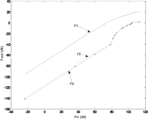
The optical link nonlinearity effects is non-existent in the 18 dB rejection configuration, and appears in the 100 dB rejection configuration, but for a very high input power value (80 dBm), which is an unrealistic input power level. It is possible to conclude, given the low-level UWB signal power, that the nonlinear effects of the optical link remain negligible during the operation of a MB-OOK system.
A study on the impact of nonlinearity of MB-OOK signals E/O transducers was undertaken by using E/O transducer nonlinear simulation models. The conclusion indicated a very limited impact, due to the low modulation indices considered, of the transducer nonlinearities on MB-OOK signals transmitted through optical fibers. Furthermore, the simulations provided the modulation power range to produce an appropriate signal to noise ratio and a low MB-OOK signal distortion level at the optical link output.
8.5.2. External modulation
In this chapter the simulations presented thus far have corresponded to direct intensity modulation. This simulation tool also allows the simulation of external modulation microwave optical links. In this case, the DFB laser is controlled by a DC biasing current. In this case the optical power envelope, which is continuous, illuminates, for example, an electro-absorption modulator (EAM) input, which can be modulated with a 40 Gb/s data rate.
The link type presented in this section corresponds to a DFB laser integrated to an electro-absorption modulator, giving an electro-absorption modulated laser (EML), the structure of which is detailed in section 2.3.7. An electrically equivalent circuit for the modulator has been developed using ADS [DES 07a]. The integration of the DFB laser electrical equivalent circuit to the EAM thus enables the modeling and simulation of the EML, i.e. the modulated optical transmitter.
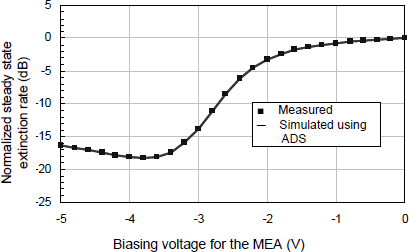
Figure 8.27 is representative of the normalized steady-state extinction rate simulated using ADS and then measured for a 75 μm modulator and a driving voltage between 0 and −5 V [GIR 09]. The experimental and simulated results superposition allows the validation of the steady-state model of an EML over the entire voltage range.
Figure 8.27. Simulated and measured normalized steady-state extinction rate of the electro-absorption modulator
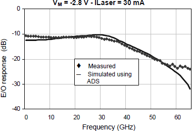
The response of the modulator electro-optic (E/O) presented in Figure 8.28 is constant in a bandwidth extended up to 36 GHz. It is sufficient for communication systems operating at 40 Gb/s. A good agreement is obtained between measurement and simulation between 100 MHz and 60 GHz.
Figure 8.28. Electro-optic modulator dynamic response
The nonlinear modulator model also enables the simulation of its response in time-domain for different electrical signals with the aid of transient analysis. When the control RF signal inserted at the modulator input is a MB-OFDM or pulse UWB data signal, the behavior of the optical modulator can be studied with the aid of ADS software. This enables an impact study to be undertaken of the E/O transducer used in radio-over-fiber systems [DES 09].
In this study, a UWB-OFDM was generated. The simulated UWBOFDM signal spectrum appearance, emitted at the modulator input, is represented in Figure 8.29. The bandwidth of the OFDM signal is 528 MHz, corresponding to a channel frequency bandwidth. This base-band-generated signal is converted by a mixer towards a central RF frequency in the desired band, which in this study was the 3.96 GHz central frequency channel, which corresponded to a low UWB channel.
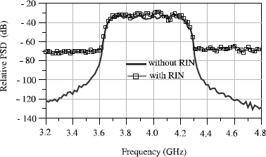
It is thus possible to simulate the power spectral density of the signal emitted at the electro-absorption modulator output thanks to a co-simulation, which, in this case, uses the data stream simulator for digital signals and the envelope simulation technique for analog signals. The simulation results (Figure 8.30) indicate a noise increase on the channels adjacent to the useful channel, especially when the noise created by the laser is taken into account in the model [DES 09]. As a result, in this case, the power ratio between the useful channel and the adjacent channels is reduced to 40 dB at the EAM output, in comparison to the 90 dB values when the RIN is removed in the laser model used.
Figure 8.29. Power spectral density (PSD) of a UWB-OFDM signal in a subchannel at the electro-absorption modulator input
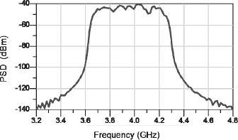
Figure 8.30. Power spectral density (PSD) of a UWB-OFDM signal in a subchannel at the electro-absorption modulator output with and without the laser RIN
The influence of the laser RIN level on the optical spectrum modulated by a UWB-OFDM is illustrated in Figure 8.31. The power spectral density at the electro-absorption modulator output is plotted for two biasing currents of 50 and 100 mA, corresponding to two measured RIN values of −147 and −157 dB/Hz, respectively, at 3.96 GHz.
Figure 8.31. The power spectral density of a UWB-OFDM signal in a subchannel at the electro-absorption output for two biasing points of the laser
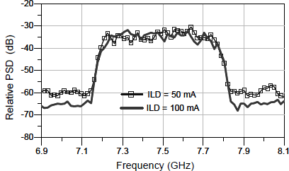
Figure 8.31 shows the decrease in noise in the adjacent channels in relation to an increase in laser biasing current for a channel of high band UWB, which has a central frequency of 7.5 GHz. This reflects the influence of RIN on the ACPR of the link.
A direct detection-external modulation RoF link, using previously presented models for the laser, the electro-absorption external modulator, the optical fiber, and the photodetector and transmitting a UWB-OFDM is simulated. The digital modulation used for each subcarrier is a 16 QAM type. The results of this transmission are explained in the remainder of this section.
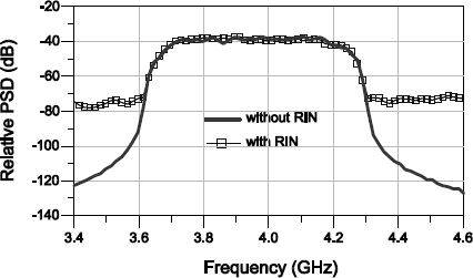
Figure 8.32 presents the spectrum of a UWB-OFDM signal at the RoF link output, demonstrating good transmission of radio data on a 100 m optical fiber. It is interesting to note that the thermal noise of the photodiode has no impact on the adjacent channels. However, the laser RIN is not negligible. The laser biasing current is equal to 100 mA for the simulations of Figure 8.32, also the attenuation introduced by the optical fiber is visible on the signal level.
Figure 8.32. Power spectral density (PSD) of a UWB-OFDM signal at the RoF link output
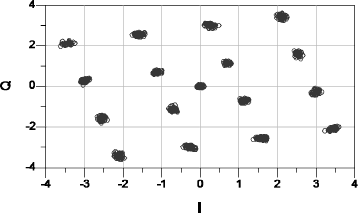
To evaluate the link performance and influence of optical components, the received signal is converted into base-band, the constellation of the received signal is plotted in Figure 8.33 when the laser RIN is removed. A phase difference is introduced along the length of the link for each symbol.
Figure 8.33. 16-QAM constellation diagram of the data received in the absence of laser RIN
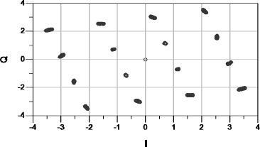
When the laser RIN is introduced in the model, the constellation diagram of the link is shown in Figure 8.34 [ALG 10]. The sprawl of each spot of the constellation of Figure 8.34 validates the fact that the RIN contributes to the phase and amplitude error increase on each received symbol. Without RIN, this error is linked to nonlinearity of the electro-absorption modulator response, which is more important for symbol values corresponding to stronger voltages (Figure 8.33).
Figure 8.34. 16-QAM constellation diagram of the data received in the presence of laser RIN (biasing current = 50 mA)
The constellation diagram of digital signals transmitted on a RoF link characterizes the phase and amplitude errors on decision points and allows the determination of the BER (bit error rate).
The simulations allow the characterization of the noise and nonlinearity of the link, and also to quantify the degradations introduced, notably by using more or less complex digital signal modulations.
8.5.3. Generation of microwave signal by frequency beating
In all the previous simulations, the optical signal is only represented by its envelope, which corresponds to the RF signal and avoids the need to simulate two very far apart frequencies (e.g. a 193 THz optical frequency and a microwave frequency in the order of tens of gigahertz). The method operates very well for a direct and external modulation microwave optical link simulation, with a single optical frequency; however, this does not allow the simulation of optical generation of microwave, as in this case it is necessary to simulate two optical signals of different wavelengths, thus different frequencies. For this case, another approach is required and the optical frequency is introduced in order to consider the component response at different wavelengths.
The two optical wavelengths are taken into account and the ADS envelope simulation is used. It analyses the signal at a certain frequency band around one of the two optical frequencies considered, these two being very close to one another.
The generation of the microwave signal is linked to quadratic detection of the two optical signals with adjacent wavelengths in the photodiode.
When two optical signals with adjacent wavelengths (which spaced out by tens of picometers) light a photodetector after transmission on a same optical fiber, the photodetected current is proportional to the square of the sum of the electric fields. It is thus proportional to the optical power expressed:
where the θ parameter corresponds to the polarization difference between the two electric fields and the τ parameter corresponds to the duration of Poynting vector time integration.
The signal after quadratic detection by a microwave photodetector has a DC component and fRF frequency component. The frequency of the microwave is proportional to the difference between the two wavelengths, λ1, and λ2, being the wavelengths of the two optical lines, such that:
[8.19] ![]()
The optical power-photodetected current proportionality factor depends on the photodetector responsivity at fRF.
The ADS envelope simulation allows simulation of the frequency range not centered on DC, but on an arbitrarily defined frequency, e.g. the optical frequency, and a simulation bandwidth in the order of twice the generated microwave frequency.
The models used for the two DFB laser sources, emitting at a wavelength of approximately 1,550 nm, are identical to those presented in sections 2.1.4 and 8.2.2. If the wavelengths of the two laser sources are at a distance of 40 pm, by applying expression [8.19], the signal generated after detection will have a frequency of 5 GHz. The photodiode model used is identical to that already presented in this chapter in section 8.2.4.
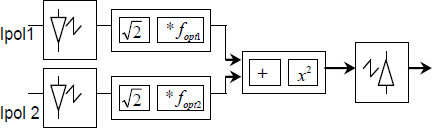
The first stage of this synoptic corresponds to two laser sources. At the input, two currents Ipol1 and Ipol2 bias the transmitting sources. At the output, the current represents the optical power of each luminous signal at two optical wavelengths spaced out by 40 pm. Then optical powers are converted into electric fields. The output signals of the second stage, having parameters homogeneous to currents, represent the electric fields of output optical signals of each of the diodes. A third block initially models the total electric field, which results from the sum of the two electric fields, then the electric field to optical power conversion is performed.
Finally, the last block is the photodetector. The output current is equal to the incident optical power multiplied by the average responsivity of the photodetector and weighted by the frequencies response of the photodetector.
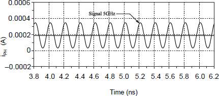
In terms of time, Figure 8.37 illustrates the simulation result of the detected microwave signal [MAN 09].
Figure 8.37. Simulation of the 5 GHz microwave signal generated by optical heterodyning
8.6. Conclusion
In this chapter, optomicrowave link simulations, principally direct modulation and intensity detection, were presented. The feasibility of the step for external modulation links was demonstrated, and optical generation of microwaves. System circuit simulation software enabling system simulation was chosen. The optomicrowave transducer was modeled by electrically equivalent circuit with the optical-microwave gain notion having been previously defined.
The benefit of this software is the ability to simulate microwave optical links in a purely microwave environment with the possibility to take into account complex digital signals as informative signals modulating the optical link, but also to extend the link study with an amplifier, e.g. low-noise amplifiers, which have their own noise and nonlinearity characteristics.
The electrically equivalent circuits of these components are defined from foundry data or MMIC circuit simulation data and provide realistic co-simulation results, which are comparable to the data obtained by measurement.
8.7. Appendix
8.7.1. MB-OOK modulation
The origin of MB-OOK modulation [PAQ 04], developed by Mitsubishi Electric ITE, is a mix of pulse and multiband approaches. It allows the coding of a single pulse with several bits. The principle consists of dividing the UWB spectrum from a pulse whose spectrum is defined in the band (3.1-10.6 GHz) as N narrow sub-bands of 250 or 500 MHz.
Figure 8.38. Transmit/receive channel of MB-OOK modulated UWB signal on the low part of UWB bandwidth
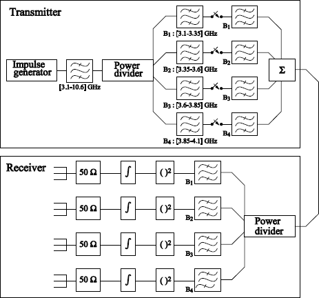
In the case of using a band reduced to (3.1-4.1 GHz), this band is divided into four 250 MHz sub-bands, which corresponds to N = 4 250 MHz band-pass filters. Thus this configuration has the ability to have four channels, each able to simultaneously transport a digital component. Figure 8.38 represents the MB-OOK modulated UWB signal transmit/receive architecture operation scheme over four channels on the low UWB.
More generally, the transmitter comprises a pulse source with a repetition frequency lower than 30 MHz, a N-way power divider, composed of N 250 or 500 MHz band-pass filters, equally distributed over the spectrum (3.1-10.6 GHz) authorized by the FCC, and N switches positioned at the N filters output, allowing the introduction of digital information coding. Each of the sub-bands is used to carry a bit by using OOK modulation. These N ways are connected to a power combiner, followed by a power amplifier then an UWB antenna for a wireless transmission path.
At the receiving part, the pulse is again divided into an identical number of different sub-bands or channels. Then, each channel is connected to a non-coherent energy receiver. For this to occur, the receiver is composed of a power divider with N ways, a 250 or 500 MHz band-pass filter on each of the N ways, a multiplier followed by a time integration of the received signal over time T, then a block allowing the digital treatment of a signal. A low-noise amplifier is positioned at the input of the receiving channel.
Each channel is used to carry a bit and the N value typically varies between 15 and 26. This allows the simultaneous transmission via a single pulse, of a symbol composed of 15 to 26 bits. The information is OOK modulated, in other words to code a “1” bit, the switch is closed and so, at the receiver, there is the presence of a signal and energy detection. However, to code a “0” bit, the switch is open, and at the receiver, there is no energy to detect. This method attains high data rates, in the order of 600 Mb/s, for a distance lower than 3 m, and 150 Mb/s for a distance of 10 m.
8.7.2. OFDM modulation
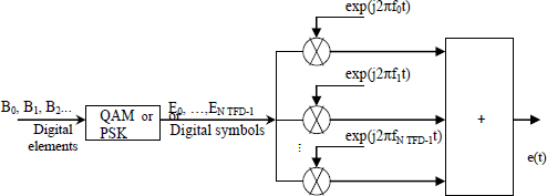
OFDM modulation is a multicarrier modulation. The novel idea of this modulation is the optimization of spectral occupation due to the orthogonality principle between subcarriers. The frequency multiplexing consists of distributing the information transmitted on a large number of sub-bands. Thus the distribution is optimal from a spectral occupation point of view, the spectrums relative to each subcarrier cover each other, providing the central frequencies of each sub-bands and the signal spectral density of the other bands is zero. This condition is called the orthogonality condition. It is important to note this orthogonality constraint between subcarriers is essential to avoid interference. This constraint applies itself in the frequency domain (gap choice between subcarriers) but also in the time domain (choice of the forming function) throughout the frequency-time duality. The most used and easiest to generate forming function is the rectangular function. The OFDM signal spectrum is thus constituted of the sum of each subcarrier spectrum spaced apart by Δf. It is interesting to note that the greater the number of subcarriers, the more the subcarriers sum spectrum tends towards a rectangular signal. Thus, an OFDM signal can be considered as a UWB signal, as the relation of the OFDM signal spectrum width on the central frequency is above 25%. The OFDM modulation operational diagram is presented in Figure 8.39.
Figure 8.39. OFDM modulation operational scheme
The mixing of digital symbols by the subcarriers, then the sum operation, can be realized thanks to the inverse discrete Fourier transform (IDFT), as schematized in Figure 8.40, and is easily implemented with the help of a fast Fourier transform (FFT). It is necessary to perform a series/parallel and parallel/series conversions before and after the IDFT.
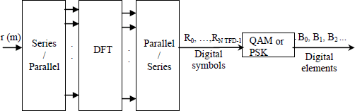
The receiving demodulation is performed by a direct discrete Fourier transform (DFT) of the received sample signal. The OFDM modulation principle has moreover known its expansion thanks to the use of this discrete Fourier transform (DFT). Figure 8.41 illustrates the OFDM demodulation principle.
Figure 8.40. OFDM modulation theoretical principle
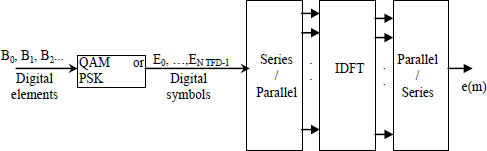
Figure 8.41. OFDM demodulation principle
The problem with perfect reconstruction of the signal arises because the convolution of the rectangular window (infinite spectrum) with a multicarrier signal (the frequency equally distributed Dirac comb spectrum) gives a signal with an infinite spectrum. Actually, the signal band transmitted is limited by a low-pass filter which does not guarantee a perfect reconstruction of the signal. However, if the number of carriers is considerable, the information lost during low-pass filtering is negligible.
The principal advantages of OFDM are the following [TRA 07]:
– the allocated frequency band use is optimal through subcarrier orthogonalization;
– the modulation uses a well known and simple algorithm: the FFT;
– an adapted coding and interweaving allow the quality improvement of data transmission;
– the cyclic prefix allows a simple equalization, particularly effective in the presence of dense multi-path channels.
OFDM nevertheless has disadvantages:
– an OFDM signal can be considered as a sum of sinusoids. The signal envelope follows Gauss’ probability law, and the probability that the signal has a large amplitude dynamic is as important as the number of subcarriers is large. This characteristic must be taken into account as soon as the amplification levels are high. The peak to average power ratio imposes that the “front end radio” unit is linear over a large power range and so its dynamic must be large;
– the subcarrier orthogonality is a key element of OFDM modulation. The phase noise or frequency difference between the local oscillators of the transmitter and the receiver implicates an orthogonality loss between the subcarriers and strong system performance decrease;
– if the OFDM receiver is badly time synchronized, an interference phenomenon between OFDM symbols can intervene, which considerably decreases the overall system performance;
OFDM systems are sensitive to imbalance between paths I and Q of the receiver and transmitter frequency transposition stages.