
Chapter 6
Complement to Microwave Photonic Link Performances
6.1. Microwave signal attenuation during double sideband modulation
6.1.1. Double sideband modulation recall
In a microwave photonic link, if the amplitude modulation occurs in the laser (direct modulation) or in a Mach-Zehnder or electro-absorption modulator (external modulation) biased at Vπ/2, as long as the modulation index is low, this modulation results in two sidebands around the optical carrier. If the optical angular frequency is ωopt and the RF angular frequency is ωRF, the electric field of the modulated wave is expressed:
[6.1] 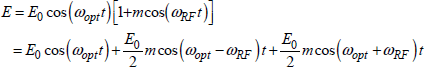
The Fourier transform of such a signal is constituted of three Dirac lines in the frequency space. E is obtained from its complex notation E1 by expression:
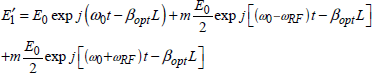
After having developed the functions of [6.1] in exponential sums, expression of E1 is given by expression:
[6.3] ![]()
6.1.2. Recall of single-mode optical fiber propagation characteristics
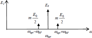
Figure 6.2 illustrates the cross-section of a single-mode fiber where the fiber core refraction index n1 is higher than the cladding refraction index n2. In a single-mode fiber, the propagation mode is the fundamental fiber mode.
Figure 6.2. Cross-section of single-mode optical fiber
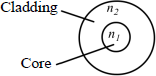
The plot of Figure 6.3 represents the development of the propagation constant β from the fundamental mode of this fiber as a function of optical angular frequency ωopt such as was obtained in section 3.1.7.
On this plot, the domain marked “F” indicates the usual fiber use zone. Point D0 (see definition below) indicates the point where chromatic dispersion of the fiber is zero. It is possible to define a certain number of parameters concerning the fundamental mode.
Figure 6.3. Optical fiber fundamental mode propagation constant
From this plot, phase velocity is given by:
Group velocity is:
The group time per unit length:
Chromatic dispersion:
and as:
![]()
The chromatic dispersion can also be written:
Around angular frequency ωopt, it is possible to write a β limited development by keeping the first three terms:
or by accounting for the fact that ωopt − ω0 = ωRF:
[6.10] 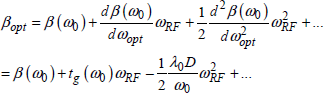
6.1.3. Optical fiber double sideband modulated signal propagation
After a travelling length L in the optical fiber, the signal phase is βoptL and equation [6.3] becomes:
By introducing the βopt limited development given by [6.10], the expression above becomes:
[6.12] 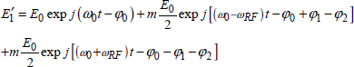
with:
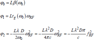
where fRF is the microwave frequency corresponding to angular frequency ωRF.
6.1.4. Double sideband-modulated signal photodetection at the optical fiber output
The passing of E’1 in a photodetector results in the production of a photodetected current:
[6.13] ![]()
where Rpd is the photodiode responsivity.
By introducing [6.12] into [6.13], the photodetected current is:
In this expression, the important term in photodetection (kept by filtering) is the cos(ωRFt) term. Regarding phase, ϕ0 is an optical phase that disappears during detection, ϕ1 is a simple phase (or delay) constant, but term φ2 acts on the photodetected current. The electrical power due to current Iph is thus proportional to cos2 φ2.
This phenomenon only appears with photodetection where optical angular frequencies (ω0 + ωRF) and (ω0 − ωRF) beat or mix separately with angular frequency ω0 to give two microwave signals that combine but are not in phase due to the chromatic dispersion.
In particular, when ![]() , expression cos2 φ2 becomes zero. This appears for a specified value of fiber length:
, expression cos2 φ2 becomes zero. This appears for a specified value of fiber length:
[6.15] ![]()
Figure 6.4 shows the development of cos2 φ2 as a function of the fiber length (in kilometers) for several frequency values (in gigahertz). Figure 8.7 from section 8.2.3 presents the same type of results (in decibels) for different microwave frequencies.
Figure 6.4. Double sideband modulation photodetected signal amplitude as a function of optical fiber length
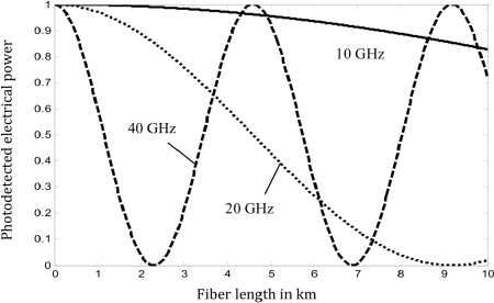
The values taken to calculate φ2 are λ = 1.55 μm, D = 17 ps/nm/km. It can be observed on this plot that the first signal cancellation occurs at 2.29 km for 40 GHz and 9.18 km for 20 GHz (see equation [6.15]).
For a 10 km length at a frequency of 10 GHz, the chromatic dispersion introduces an electrical attenuation a little less than 1 dB, obviously acceptable for the optical attenuation of 0.2 dB/km.
Even for very short links, the evanescence effects are felt. In Figure 8.7 of section 8.2.3 an optical fiber with a chromatic dispersion of 17 ps/nm/km and a millimeter wave spectrum frequency of 60 GHz, the total evanescence intervenes for a 1 km fiber length. This result implies that for a 60 GHz double sideband modulation to have an acceptable attenuation, the fiber must not be over 100 m. This illustrates the benefit of using the techniques discussed in the following sections and allows the use of only two optical lines, e.g. by removing the optical carrier [WEI 08].
6.2. Modulator structures for optical carrier or high and low sideband removal
6.2.1. Optical modulation recall
As recalled at the beginning of Chapter 2, the direct optical wave modulation by the source laser or by an external modulator gives rise to double sideband modulation. It was shown in the previous section that the chromatic dispersion of the fiber can lead to an evanescence of the microwave modulation signal after detection, even in short links with a 60 GHz RF. This evanescence comes from the simultaneous detection of the beating or mixing between the optical carrier and each of the lateral lines in the presence of chromatic dispersion. To avoid this detrimental effect, which is due to the presence of three lines, one of the lines must be eliminated.
One solution consists of high or low single sideband modulation of the optical carrier. In this case, the evanescence of the modulation signal is removed.
Another solution consists of removing the optical carrier, which results in only two sidebands and, therefore, no more evanescence. This time, the detection shows a microwave signal of double frequency. This can be advantageous to overcome modulator frequency limitations.
The final possibility is to remove a sideband and the microwave carrier. This results in the presence of only one sideband line to which a new optical carrier can be added. This type of device now allows a change in microwave signal frequency.
Each of the cases listed above correspond to different modulator configurations, but these different configurations cannot be obtained with direct laser modulation. These configurations must always use external modulator combinations. This aspect limits the feasibility of these solutions if the modulators are discrete components. In the case of an integrated microwave photonic link, the solutions presented below can be possible and will lead to more cost-effective solutions in the future [LAM 06].
6.2.2. Single sideband or carrier suppression optical modulators
When the carrier is a microwave signal, the different amplitude microwave modulator configurations are known so that a low or high single sideband or carrier suppression modulations can be obtained. These configurations are presented in [RUM 04d].
From the same principle, different configurations are possible with an optical carrier. The general diagram possibilities from Mach-Zehnder modulator cells are presented in Figure 6.5.
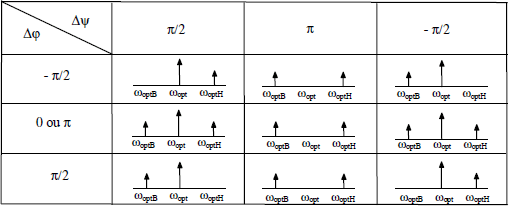
From the general schemes of Figure 6.5, Table 6.1 lists the different possibilities. The optical ψ and electrical φ phases are illustrated in Figure 6.5a. Another possibility is to adopt the configuration of Figure 6.5b. In this case Δψ = Δψ/2 −(−Δψ / 2)and Δφ = Δφ / 2 −(−Δφ / 2). In Table 6.1, ωoptB = ωopt — ωRF and ωoptH = ωopt + ωRF.
For a Mach-Zehnder modulator, the phase difference of 0 on the microwave signal corresponds to a modulator such as that studied in section 2.2. Phase difference Δψ is obtained, for example, by biasing each electrode of a Mach-Zehnder modulator with a continuous voltage, e.g. for Δψ =π/2, the biasing voltages are Vπ/2 for Figure 6.5a and + Vπ/4 and -Vπ/4 for Figure 6.5b.
Figure 6.5. General configuration of a single sideband or carrier suppression modulator with a) a phase difference in one branch or b) balanced phase differences
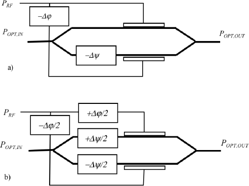
Table 6.1. Δψ (optical) and Δφ (electrical) phase difference effects on the optical carrier and low ωoptL and high ωoptH sidebands
A carrier suppression Mach-Zehnder modulator is presented in [WEI 08]. A Mach-Zehnder modulator biased at Vπ is used to generate at the optical fiber output, a 60 GHz wave from a 30 GHz modulation. The limitations to an acceptable length of 100 m of a 17 ps/nm/km dispersion fiber (see evanescence at 1 km Figure 8.7) can thus be extended to 5 km.
Figure 6.6. Configuration used in [SMI 97] for a high single sideband modulation
Optical carrier suppression modulator configurations are also included in the structures of the following section.
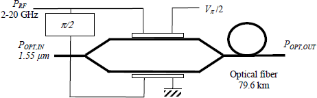
An example of a single sideband modulator is given in [SMI 97]. The scheme in Figure 6.6 summarizes the used configuration. The dual-type Mach-Zehnder modulator schematized in this figure is fed by a 1.55 μm optical wavelength optical signal and a power of -2 dBm (DFB laser).
The modulator is biased and excited to perform a double sideband classical modulation. For this, one of the electrodes is biased at an average potential difference of Vπ/2and the other is earthed. The RF signal is applied in phase on each of the electrodes. The 79.6 km of optical fiber partly induces a normal attenuation of 18 dB (compensated by an optical amplifier), but also evanescence (total signal disappearance) at frequencies of 6.6, 11.8, 15.2, and 17.9 GHz.
If the microwave signal phase difference is π /2 between the two electrodes, the high sideband is selected and the low sideband is eliminated. As a result there is no microwave signal evanescence after detection. Due to the inaccuracies in the phase differences only an attenuation of 1.5 dB remains.
A 50 Mb/s signal transmission demonstration is thus performed on a 12 GHz microwave subcarrier (one of the evanescence frequencies in double band modulation).
6.2.3. Carrier suppression and single sideband optical modulator
Amongst several realizations [IZU 81; SHI 01], a carrier suppression and unique sideband modulator example is presented in Figure 6.7 for “x-cut” modulators [HIG 01]. The modulator representation is diagrammatic. Two carrier suppressed modulators (1 and 2) are connected in parallel. The carrier suppression is obtained by introducing a π optical phase difference between the two tracts (see Figure 6.5). These two modulators are then recombined by an optical connection including a π/2 phase difference (this phase difference can be inserted before or after the second modulator with identical results). These two phase difference types (π and π/2) are obtained with the help of electrodes on which a continuous biasing of Vπ or Vπ/2 is applied. The microwave signal is then applied in phase on the electrodes of a same modulator (1 or 2) but with a π/2 phase difference between them. The optical wavelength is 1.55 μm and the microwave frequency is 10 GHz.
As seen in section 2.2, the modulation of an optical frequency v by a microwave frequency fRF introduced by lines ν, ν + fRF, ν−fRF, ν + 2fRF, ν −2fRF, ν + 3fRF, ν − 3fRF, etc. the relative amplitudes of which are described by Bessel functions marked by terms: J0, J−1, J +1, J−2, J +2, J−3, J +3, indices ±1, ± 2, ± 3 represent ± fRF, ± 2 fRF, ± 3fRF in connection to the optical carrier.
In the example of Figure 6.6, modulators 1 and 2 each eliminate the optical carrier (J0) and the microwave signal harmonic pair (J−2, J +2, J−4, J +4). Then the combination of the two modulators strengthens J +1 and eliminates J−1. A more detailed analysis shown in the configuration of Figure 6.7 also strengthens J−3 and J5 but eliminates J3 and J−5 at the same time.
In order to substantiate these results, the configuration of Figure 6.7 was simulated using COMSIS software [COM 03; LAM 06] with a 1 GHz microwave frequency. The results are presented in Figure 6.8 where it is possible to observe the elimination of the optical carrier and line J−1, the strengthening of J+1 and also J−3. The amplitude ratio between these two lines is greater than 30 dB. The measurements performed on the structure in Figure 6.7 [HIG 01] show that for a 10 GHz modulation and for a practical realization introducing imperfections, the ratio stays greater than 25 dB.
Figure 6.7. Configuration used in [HIG 01] for a carrier suppressed single sideband optical modulation
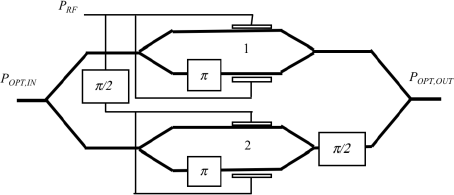
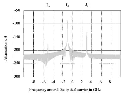
Finally, both the simulations [LAM 06] and the performed measurements in [HIG 01] show that the π/2 optical phase difference of modulator 2 to modulator 1 (after or before this modulator) induces the reversal of results illustrated in Figure 6.8. It can be observed that J0 is always eliminated, but this time J−1 and J3 are strengthened. The 30 dB ratio between J−1 and J3 remains.
After these modulators, there remains only one optical line. It is now possible to introduce an optical carrier with a wavelength different from the one that was eliminated and to produce a change in the microwave frequency.
In the examples given below, the modulators were realized on lithium niobate and the optical phase differences were realized with continuous voltage differences applied on the electrodes. These structures remain costly using current technology. However, as recalled at the beginning of this section, optical phase differences can be realized in micro-photonic structures, possibly with micro electromechanical systems (MEMS) adjustment techniques. This solution may still require extensive development, but it allows the possibility of much less costly structures.
Figure 6.8. Simulation [LAM 06] of a carrier suppressed single sideband optical modulator presented in [HIG 01]
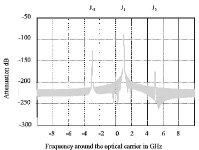
Figure 6.9. Simulation [LAM 06] of a carrier suppressed single sideband optical modulator presented in [HIG 01] by transferring the π/2 optical phase difference from modulator 2 to modulator 1 of Figure 6.7
6.3. Degradation of a microwave signal spectral purity by an optical link
6.3.1. Phenomenon description
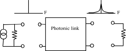
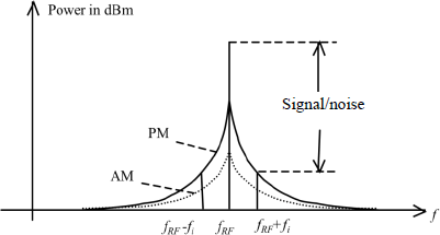
The transmission of a microwave signal over a photonic link can be used to distribute a reference frequency and, in this case, the spectral purity of the transmitted signal is of great importance. However,spectral purity degradation can also affect the transmission of a digital signal by a microwave frequency itself transmitted by an optical link. This transmission is performed by an optical signal intensity modulation followed by direct photodetection of this signal (IM-DD link). Under these conditions, the laser line width producing the optical wave has no effect on the spectral purity of the transmitted microwave. However, if a perfect microwave is transmitted by an optical link, its spectral purity suffers degradation in both amplitude and phase as illustrated in Figure 6.10.
Figure 6.10. Spectral purity deterioration of microwave signal transmitted across an IM-DD photonic link
From the laser presentation (section 2.1.8), it was recalled that laser noise presents a very strong 1/f increase at low frequency. It is the transposition of this RIN in 1/f increase around the microwave signal modulation that induces the appearance of amplitude and phase noise around the microwave frequency at the laser output. This effect was studied in [BIB 98], but before presenting the results of this work, it is useful to recall some definitions concerning the noise around the microwave carrier.
6.3.2. Some definitions concerning the noise around a microwave carrier
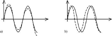
From a sinusoidal microwave signal, Figure 6.11 shows the amplitude (amplitude noise) and phase (phase noise) fluctuations.
Figure 6.11. Microwave signal a) amplitude and b) phase fluctuations
The microwave with both amplitude and phase fluctuations can be written:
The two fluctuations ΔARF (t) and ΔφRF (t) produce a noise spectrum around the microwave carrier. At distance fi from the carrier (angular frequency ωi), the amplitude and phase disruptions can be represented by a Fresnel diagram as in Figure 6.12. There is no reason for the phase and amplitude noises to be identical. This is indicated in this figure.
Figure 6.12. Fresnel diagrams of amplitude and phase of microwave (ωRF) fluctuations at ωRF + ωi and ωRF — ωi frequencies
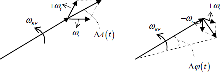
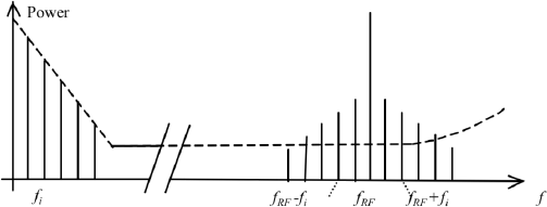
Figure 6.13 illustrates the position of the two frequency lines fi after the Fourier transform in relation to the frequency of the microwave (fRF).
Figure 6.13. Characterization of the deterioration of the signal to noise ratio around a microwave frequency
Using the definitions above, it is possible to evaluate the spectral densities of amplitude and phase fluctuations. The total spectral density of the fluctuations is the sum of the single band spectral densities. As the measurements are made after frequency change, around frequency 0, and in the area of the positive frequencies, the measured values correspond to twice the spectral densities measured in each of the sidebands around ωRF.
The fluctuation spectral densities are measured in a 1 Hz band. The in-phase fluctuation spectral densities are expressed in rad2/Hz and the amplitude spectral densities are expressed in V2/Hz.
The spectral purity is computed by calculating the ratio between the power of the microwave carrier and the total noise fluctuation densities. It is expressed in dBc/Hz. Knowledge of the total power of the noise implies that the amplitude or phase noises are known, except in the case where one of the two fluctuations is predominant.
6.3.3. Amplitude and phase noise in an optical link
If an average current, I0, is applied to a laser, the optical power at the output optical can be detected by a photodetector and gives rise to a current Iph. If a microwave current of amplitude i1 is added to this continuous biasing, the photodetected current amplitude is mIph where m is the modulation index with: m = i1/Iph. However, amplitude and phase fluctuations due to the laser appear at the output (it is assumed that the contribution of photodetector noise is negligible). The laser RIN is equally distributed in amplitude and phase but the low-frequency noise transposition around the ωRF angular frequency of the microwave signal is added. The phase noise contribution to ωRI ± ωi angular frequencies is written 〈ΔΦ1 (ωi)2〉, which represents Φ1 phase fluctuations due to current i1. The amplitude for the same ωRF ± ωi angular frequencies, is written 〈ΔP1 (ωi)2〉. It is possible to deduce the phase and amplitude noise powers using the following equations:
[6.17] ![]()
where kdet is the V/radian detector conversion factor, which transforms phase fluctuations into applied potential difference fluctuations at a resistance R. If the applied signal power is ![]() , it is possible to define the relation between phase L(F) or amplitude M(F) noise power and applied power:
, it is possible to define the relation between phase L(F) or amplitude M(F) noise power and applied power:
where RIN (ωRF, ωi) is the low-frequency laser RIN.
In the following sections, the amplitude and phase microwave signal modulations are computed and the characteristics of these fluctuations are compared with those of the above expressions.
6.3.4. Phase noise computation of a microwave signal transmitted by an optical link
The transposition of the low-frequency increase of laser RIN around microwave signal modulation induces a noise increase of this microwave signal both in amplitude and phase. This is illustrated in Figure 6.14 where it is shown that laser RIN at a frequency fi(LF) is transposed to the fRF + fi and fRF− fi frequencies. In reality, the LF noise is continuous as a function of frequency, and its representation in a series of lines is a trick to better understand the phenomenon but which can also be used to perform simulations.
Figure 6.14. Illustration of the transposition of LF noise of frequency fi to frequencies fRF ± fi
It will be seen in section 8.3.1.1, it is possible to establish a complete nonlinear laser model from physical and phenomenological parameters. It is these parameters that are used to establish expressions giving the low frequency noise conversion of a particular laser to amplitude or phase noises, which degrade the spectral purity of the modulation frequency [BIB 98; BIB 99]. Whereas amplitude noise (following paragraph) results from the beating or mixing between low-frequency noise increases and the microwave signal, phase noise is more an AM/PM conversion of this noise. The corresponding expressions are therefore quite different.
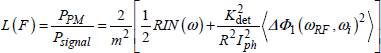
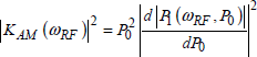
Concerning phase noise, the AM/PM conversion produces noise that is proportional to the average optical power in the laser, but this does not depend on the amplitude of the microwave signal. Expressions have been given in [BIB 99] for the phase fluctuations starting from equation [6.17]:
[6.21] 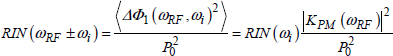
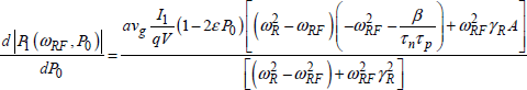
with:
and:
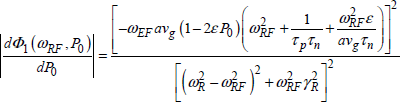
where ωR and γR have different definitions to those given for ΩR and ГR in equation [2.19]:
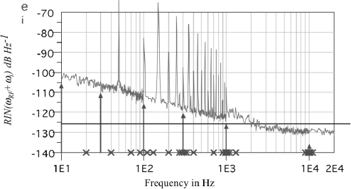
The simulated value of phase noise (see equation [6.21]) is plotted in Figure 6.15 as a discrete series of lines for the same laser simulated as in section 2.1.10.
Figure 6.15, taken from [BDE 06], shows transposition simulations of a LF intensity noise in phase noise around a 4 GHz signal modulation (discrete lines), as well as a RIN noise simulation around this 4 GHz frequency (horizontal line) and for a biased current of 60 mA. This same figure also shows the phase noise measurements.
It should be noted that this noise does not depend on the amplitude of the modulated signal so in this figure it is normalized by the square of the continuous power emitted by the laser.
Figure 6.15. Transposition of laser LF intensity noise into phase noise around the microwave signal for a 60 mA current: simulations and measurements
6.3.5. Amplitude noise computation of a microwave signal transmitted by an optical link
The transposition between the RIN BF increase and microwave signal is performed by a beating or mixing that restores amplitude noise around the microwave signal. Amplitude or intensity noise fluctuations are represented by the following expression [BIB 98]:
with:
and:
where:
This time, as it is the result of a mixing, the expression of noise contains the applied microwave current amplitude. Thus, this noise is proportional to the microwave signal amplitude I1, meaning that it can be very low if the modulation index m is low.