Electro-Optical and Piezoelectric Applications of Zinc Oxide
ZnO is an emerging nanoscale material due to its exciting optoelectronic and piezoelectric properties. In Chapter 7, ZnO is discussed in detail. The growth of nanoscale ZnO films is presented, along with the resulting optoelectronic properties of these materials. The principles of piezoelectricity are introduced, along with ZnO-based generation of electricity through force.
Keywords
ZnO; epitaxial growth; ZnO nanowires; piezoelectricity; ZnO nanogenerator
7.1 Optoelectronic Applications
7.1.1 Optical Properties of Zinc Oxide [1]
Apart from III–V nitrides and II–VIII–VI selenium compounds, the unique nature of zinc oxide (ZnO) makes it a much anticipated material for the next generation of wide band-gap semiconductor laser devices. Although the methods for preparing ZnO of higher quality have yet to be further explored, ZnO has shown great superiority over other materials. Zinc oxide is considered to be an important direct wide band-gap semiconductor material. At room temperature, it can have a band-gap width of 3.37 eV and exciton binding energy of up to 60 meV, with rotation properties from the blue to ultraviolet bands. ZnO has high chemical and thermal stability and is not easily oxidized in the atmosphere. Compared with III–V nitrides and II–VIII–VI selenium compounds, it has unmatched material stability.
Because the ZnO grain size goes down to the nanoscale, significant changes will occur on its surface electronic structure and crystal structure, and thus it will show nanoscale size effect, surface effect, dielectric confinement effect, and quantum size effect that macro-block materials do not have. Meanwhile, it may have characteristics unparalleled in normal ZnO materials. Many of its special features can be applied in a variety of areas, including chemistry, electronics, biology, and medicine.
Zinc oxide-based semiconductor optoelectronic devices, including UV detectors, light-emitting diodes (LEDs), and semiconductor laser diodes (LDs), are widely used in optical communication networks, optical display and storage, conversion, and optical detection. In the field of optoelectronic displays, for example, the technology for flat panel displays is a basic requirement for the terminal display in the information age. Currently, it is available with key technologies, including liquid crystal display, cathode ray tube, plasma display panel, vacuum fluorescent display tube, and LED. The LED for flat panel displays exhibits the advantage of low drive voltage. Combined with IC design, it is secure in use, featuring a multicolor display, long life, and quick response. As an ideal flat panel display device, it has a wide range of potential applications for scientific instruments, portable computers, and aerospace and military fields. Commercialized red and green LED monochrome display devices have been available, yet color displays are not commercialized. The main reason is that the brightness and color purity of blue electroluminescence is lower than required, making it unable to display true colors with three primary colors, whereas white electroluminescent materials are mostly in the broadband radiation, which cannot satisfy the practical requirements because of lower effective radiation intensity of three primary colors from the filter chips. This is known as the blue electroluminescence problem in the field of electroluminescence. The development of the zinc oxide-based LED makes it possible to produce full-color LED displays, launching a blue electroluminescence boom worldwide.
The key technology for ZnO-based optoelectronic devices is the preparation of high-quality p-type ZnO thin films. Intrinsic ZnO is an n-type semiconductor, which must be doped with the acceptor before p-type transformation is achieved. However, there are more donor intrinsic defects in zinc oxide; they may produce a high degree of self-compensation effects on acceptor doping. Also, acceptor impurities in solid solution are very low; it is difficult to achieve p-type transformation, resulting in failure in making the core of semiconductor devices with a zinc oxide p–n junction structure. This greatly limits the development and application of zinc oxide-based optoelectronic devices. At present, p-type ZnO research has become an international focus, and a series of breakthroughs have been made accordingly. A ZnO homogeneous p–n junction with a two-tier structure of p-ZnO/n-ZnO has been created. In addition, some proposals like the donor–acceptor co-doping method that can be used to reduce acceptor ionization energy, resulting in the formation of shallow acceptors in ZnO, have been proven to be feasible [2]. These results have great significance for new attempts at making zinc oxide short-wavelength light-emitting devices, performing in-depth studies, and applying the doped ZnO thin-film crystal growth mechanism to broaden the application areas of zinc oxide thin films.
In recent years, blue–green lasers have become popular in semiconductor laser research. As early as 1991, the US-based 3M Company achieved the first II–VI ZnSe-based quantum-well laser (77 K), which was breaking news in the field of science. After that, the joint study group of Brown at Purdue University in the United States, Philips in the Netherlands, and Sony Corporation in Japan made lasers that could work continuously at room temperature. By 1996, Sony Corporation showed its II–VI blue–green laser, with ZnSe/ZnCdSe as quantum wells and ZnMgSSe as the restriction layer, had a continuous working life at room temperature up to 100 h. However, the development of ZnSe-based lasers has not been as fast as many had expected. A full 5 years were spent improving the laser’s working life from 1 to 100 h, but further enhancements might lead to even greater difficulties. The main reason lies in the fact that ZnSe crystals have strong ionic and weak covalent characteristics. It is very “soft” and easily damaged. Under stimulated emission, it can easily have a large number of defects in proliferation due to an increase in temperature. It generated many doubts among researchers, who wondered if ZnSe, with its inherent shortcomings, is suitable for making a blue–green laser. In particular, after 1996, with the emergence of GaN blue LEDs and LDs, the ZnSe material series was facing bleaker prospects. Since the success of GaN lasers in continuous operation at room temperature, negative views of the blue–green laser in the ZnSe system have prevailed.
Are the II–VI semiconductors in dire straits regarding creating a blue–green laser? Some research groups still continue to improve the quality of ZnSe epitaxial material (such as the use of a ZnSe single crystal as the substrate, reducing the misfit dislocation of the ZnSe/GaAs interface) and increase the concentration of p-type doping and perfection of the ohmic contacts of the electrode. In addition, there are still two ways for new exploration. One is the use of the beryllium compound ZnMgBeSe. However, many people might hold back considering its highly toxic nature. The second way is to use ZnO materials.
Currently, zinc oxide at room temperature can be observed to have stimulated emission by optical pumping. Yet the observation of stimulated emission at low temperatures by using electron beams in ZnO bulk materials has been seen for many years. However, because of the fact that stimulated emission intensity is rapidly reduced with an increase in temperature, ZnO optoelectronic material has long been neglected by researchers. Because the GaN system has provoked more attention in recent years, ZnO material has been used as a buffer layer between the GaN epitaxial layer and the SiC substrate. The reasons are attributed to the following basic properties. First, ZnO shares the same wurtzite-type lattice structure as that of GaN. Its a-axis lattice constant is 0.325 nm, which is less than 2% of the lattice mismatch with GaN, and its c-axis lattice constant is 0.527 nm. Second, ZnO has an n-type doping concentration up to 1019/cm3 and mobility of 260 cm2/Vs, showing excellent electrical properties. Third, according to the common anion rule of electron affinity and energy band offsets, ZnO has a conduction band minimum that is lower by 0.7 and 0.4 eV respectively than those of GaN and SiC. Therefore, its use as a buffer layer between GaN and SiC will not cause a barrier to block electron motion. In the usual GaN/AlN/SiC structure, the buffer layer of AlN has a conduction band offset of 2.1 and 2.4 eV from GaN and SiC respectively, resulting in the buffer layer AlN becoming a potentially high electronic barrier. Finally, compared with the nitride semiconductor, ZnO material is quite soft and has a relatively small shear modulus. Its use as a buffer layer can prevent the dislocation caused by the lattice mismatch extending to the GaN active layer.
7.1.2 Epitaxial Growth of ZnO
Because ZnO bulk material tends to have some flaws, stimulated emission can only be achieved under low-temperature conditions. Therefore, it is not appropriate to use it for making different devices. The use of epitaxial thin films or a low-dimensional quantum structure is thus necessary to improve the crystal quality and the bound exciton energy. So far, high-quality growth of ZnO is accomplished by the use of molecular beam epitaxy (MBE) technology, with (0001) Al2O3 as the substrate. Although ZnO and Al2O3 may have a lattice mismatch of up to 16%, strain release could lead to a three-dimensional growth of ZnO quantum dots. In the process of growing ZnO in MBE, one of the greatest problems is the O2 that may find a way into the growth chamber. The following is a brief overview of two kinds of technologies for MBE growth of ZnO.
7.1.2.1 MBE Technique with Microwave
Because the binding energy of oxygen molecules is as high as 5.16 eV, the traditional methods for material growth, for example MBE and chemical vapor deposition, are unlikely to decompose oxygen molecules into atoms. Here, one of the simplest ways is to decompose oxygen molecules into atoms before they react with Zn and, in this way, the flow of O2 will also be reduced. A research team in Japan at the Tohoku Institute of Metallic Materials made a clever use of microwave methods that allowed oxygen molecules to be ionized into the plasma before passing into the growth chamber, where the microwave source power was 120 W, gas flow was controlled by a drain valve, the selected substrate was (0001) sapphire, and growth temperature was maintained at 500–550°C.
7.1.2.2 L-MBE Growth Technique
Another growth technique is the high-power laser ablation of the ZnO target with a purity of 99.999%, so that ZnO can be sputtered onto (0001) sapphire substrates at a temperature of 500°C. In this growth process, ZnO decomposition is inevitable under high-power laser and high local temperature. To ensure the quality of crystals, the growth chamber requires an oxygen-rich environment. In general, we can use the beam pressure of oxygen to increase the level of oxygen.
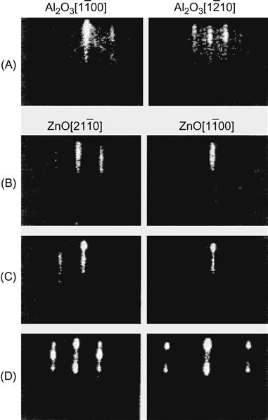
These two methods for epitaxial ZnO on sapphire are executed by using the Stranski–Krastanov growth mode. The whole process is monitored by high-energy electron diffraction. In the initial stage of epitaxial ZnO, the thin stripe-like RHEED pattern shows that the growth is in a two-dimensional layer. As the ZnO thickness increases, strain energy in the epitaxial layer accumulates to a certain degree and will be released by way of dislocation, thus forming a three-dimensional growth nucleus. At this point, some dots in the RHEED pattern will be distributed on the thin line as shown in Figure 7.1. Epitaxial ZnO may have the [![]() ] and [
] and [![]() ] crystal orientations that are, respectively, parallel to the [
] crystal orientations that are, respectively, parallel to the [![]() ] and [
] and [![]() ] of Al2O3. Because ZnO thickness is 55 nm, images under the atomic force microscope show the regularly ordered microcrystalline islets formed in three-dimensional growth with a diameter of approximately 50 nm and fluctuation of 10%. Compared with the bulk material, these two methods can reduce the concentration of impurities and defects so that stimulated emission may occur at room temperature. It should be made clear that in the growth of InAs on GaAs substrates, the lattice constants of both have a difference of 7%. Because the InAs layer thickness is approximately 0.5 nm, the formation of islets starts. The mismatch between the ZnO and Al2O3 may be 16%, whereas the critical thickness of the formed islets is 55 nm. This might be determined by three factors: ZnO surface energy, Al2O3 substrate surface energy, and the interfacial energy between the two.
] of Al2O3. Because ZnO thickness is 55 nm, images under the atomic force microscope show the regularly ordered microcrystalline islets formed in three-dimensional growth with a diameter of approximately 50 nm and fluctuation of 10%. Compared with the bulk material, these two methods can reduce the concentration of impurities and defects so that stimulated emission may occur at room temperature. It should be made clear that in the growth of InAs on GaAs substrates, the lattice constants of both have a difference of 7%. Because the InAs layer thickness is approximately 0.5 nm, the formation of islets starts. The mismatch between the ZnO and Al2O3 may be 16%, whereas the critical thickness of the formed islets is 55 nm. This might be determined by three factors: ZnO surface energy, Al2O3 substrate surface energy, and the interfacial energy between the two.
7.1.3 Optical Properties of ZnO Quantum Dots
With the ZnO band gap of 3.37 eV, stimulated emission may be achieved at low temperatures. Nonetheless, such stimulated emission has never been observed at room temperature, and thus it is of little scientific interest to the research community. By the time ZnO quantum dots were successfully grown, the optically pumped stimulated emission observed at room temperature may achieve an exciton binding energy of 60 meV. Such high energy at low temperatures makes it possible to significantly reduce the lasing threshold. The following is a brief description of optically pumped stimulated emission of ZnO quantum dots.
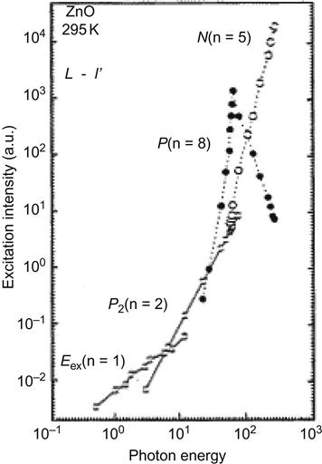
With the cwHe–Cd (355 nm, 15 ps) laser as the excitation light source, a different composite process can be observed at different excitation intensity, as shown in Figure 7.2.
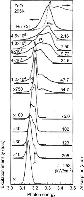
The free exciton peak A in Figure 7.2 corresponds to the stimulated emission peak Eex at low-intensity excitation. In the case of higher excitation intensity, the free exciton peak may be gradually replaced by a new P2 peak of approximately 70 meV, which is lower than Eex. This is a spontaneous emission peak in the collision process of two excitons, the intensity of which presents a linear increase as the optical pump intensity increases. In the collision process of the two excitons, one of the excitons will absorb energy from another exciton and complete the transition to the high-energy state Pn. The exciton will release a photon in the transition from an unstable high-energy state back to the ground state.
(7.1)
Here, ![]() ≈60 meV is the binding energy of the ZnO exciton, k is the Boltzmann constant, and T is the temperature. When the optical pump intensity reaches the threshold
≈60 meV is the binding energy of the ZnO exciton, k is the Boltzmann constant, and T is the temperature. When the optical pump intensity reaches the threshold ![]() , the P2 peak is gradually replaced by the new stimulated emission peak P, with the optical pump intensity increased further to the threshold
, the P2 peak is gradually replaced by the new stimulated emission peak P, with the optical pump intensity increased further to the threshold ![]() , and a new stimulated emission peak N will appear. For the relationship between stimulated emission intensity L and optical pump intensity I, see Figure 7.3. As the excitation intensity exceeds the threshold
, and a new stimulated emission peak N will appear. For the relationship between stimulated emission intensity L and optical pump intensity I, see Figure 7.3. As the excitation intensity exceeds the threshold ![]() , the peak P intensity may decrease with the increase of excitation intensity. This is because the excitation light source is too strong, thus resulting in high concentrations of plasma.
, the peak P intensity may decrease with the increase of excitation intensity. This is because the excitation light source is too strong, thus resulting in high concentrations of plasma.
7.1.4 Controlled Synthesis of the Ordered ZnO Nanowire Arrays
As one of the one-dimensional ZnO nanomaterials, ZnO nanowire plays a key role in the development of devices using ZnO-based nanomaterials. The process of producing ZnO nanowires is a key issue worldwide. To date, scientists have invented many new techniques and new methods for preparing ZnO nanowires. The growth mechanism of ZnO nanowires can be categorized in the following ways: (1) vapor–liquid–solid (VLS) growth method, (2) vapor–solid (VS) growth method, and (3) hydrothermal method. These methods can be classified as follows.
7.1.4.1 VLS Growth
In the 1960s, R. S. Wagner and associates first proposed the VLS growth method in their research on the growth process of silicon whiskers. This is the traditional method for the growth of one-dimensional material. It is based on the catalyst of liquid metal clusters as the active sites of gas-phase reactant. The source material for preparation of the one-dimensional material is heated into vapor form. After the vapor is spread onto the surface of the catalyst to form saturated clusters, one-dimensional nanostructures will grow and take shape on the catalyst surface. The VLS method has been widely used for the preparation of nanowires of various inorganic materials, including ZnO nanowires. In the thermal evaporation VLS growth method for preparation of one-dimensional zinc oxide nanomaterials, catalysts are often made from copper or gold, or nanoparticles or nanofilms prepared with other transition metals.
Based on the catalytic VLS growth mechanism, ZnO nanowires can be synthesized using a simple chemical vapor transport and condensation method. Here, the catalyst plays a vital role in the growth of ZnO nanowires. By controlling the starting position and size of the catalyst, control of the location and diameter, respectively, of ZnO nanowires can be achieved, whereas the density of nanowires can be controlled by the density of catalyst particles. However, using the current catalyst VLS method, we cannot control the size and density distribution; therefore, we cannot control the diameter, location, and density distribution of ZnO nanowires.
7.1.4.2 VS Growth
The VS method includes one or several reactants heated to form vapor at high temperatures. The vapor in an inert gas flow is transported to the low-temperature zone in the reactor or vapor is rapidly cooled to achieve growth in one-dimensional structural materials. In 1997, Yang and colleagues used the improved VS method and successfully prepared an MgO nanorod array with a diameter of 7–40 nm and height of 1–3 μm. The preparation of one-dimensional zinc oxide nanomaterials using the VS growth mechanism is also very common. Lee and colleagues, by controlling the atmosphere, prepared ZnO nanowires by way of thermal evaporation, where zinc oxide powder was used as raw material with no catalysts and thermal evaporation temperature was 1,380°C. Nanowire growth substrate was placed at the export end of an alumina tube at a temperature of approximately 450°C. Xu and associates prepared ZnO nanowires and nanowhiskers with calcined ZnC2O4 nanoparticles and powders. Surface-active agent was used in the calcination process. In a tube-type furnace, the quartz boat had a temperature of 920°C and access to ammonia. The growth of ZnO nanowires is also interpreted as the VS mechanism in this preparation method.
The VS method has the advantage of requiring no catalyst; however, considering the complexity of the equipment for the synthetic process, the higher reaction temperature, very limited choice of substrate, the expense, and difficulty in controlling the size and shape of one-dimensional material, it is greatly limited in applications in the manufacture of devices.
7.1.4.3 The Hydrothermal Method
The hydrothermal method is in the liquid-phase synthesis method category.
The liquid-phase synthesis method, compared with VLS and VS, which require high temperatures (800–1,400°C), is a low-cost, low-temperature synthetic method. The hydrothermal method was first used for synthesis of ZnO nanorods. Zn nitrate solution (Zn(NO3)2•4H2O), mixed with hexamethylene tetramine, is placed inside a hydrothermal reactor at 95°C and heated for 1–10 h. From sediment on the F–SnO2 glass after cleaning and air-drying, a large number of aligned ZnO nanorods can be obtained; however, the size of the product is a bit too large. There are improved methods, such as the two-step hydrothermal method. The two-step hydrothermal method is as follows. First, ZnO grains with a diameter of 5–10 nm are evenly scattered on an Si (100) chip as a crystal seed. When the silicon chip is uniformly covered, ZnO nanorods can be synthesized at 90°C by shaking the chip suspension for 0.5–6 h in an open crystalline plate of zinc-filled nitrate solution. After the chip is removed with salt ions, cleaned, and dried, we can get ZnO nanorods with a diameter of approximately 90 nm. In addition, the hydrothermal synthesis method can also be used to prepare ZnO nanowires. Currently reported array films of single-crystal ZnO nanorods created by a hydrothermal preparation have a highly consistent orientation, with an average diameter of approximately 40 nm. The film of approximately 390 nm emits strong fluorescence. A ZnO nanocolumn array created by hydrothermal synthesis has a nanocolumn length of 230 nm and a diameter of 38 nm. ZnO nanowire created by hydrothermal synthesis has a diameter of 50–80 nm and a length of more than 6 mm.
Compared with the preparation method of ZnO nanowires as described in Sections 7.1.4.1 and 7.1.4.2, the hydrothermal method has the unique advantages of being simple and economical and requiring no special large-scale equipment or high reaction temperature. If the size and location of ZnO grains (precursor of ZnO nanowires) can be controlled, then the ZnO nanowire size, location, and orientation, which are ultimately obtained with the hydrothermal method, can be controlled by the homoepitaxy principle.
7.2 Piezoelectric Applications of Zinc Oxide
7.2.1 Piezoelectric Effect
In physics, a number of dielectric ionic crystals (e.g., quartz, Rochelle salt, barium titanate) will have polarization not only under an electric field but also under mechanical stress.
In a certain direction, as the dielectric experiences a mechanical force to deformation, it will cause the relative transfer of its internal positive and negative charge centers to polarize. As a result, two of its relative surfaces (polarization surfaces) will be found with the bound charge Q with the opposite symbols, and its electric displacement D (the charge density σ in the MKS system of units) is proportional to the external stress tensor T:
(7.2)
In this equation, d is the piezoelectric constant matrix. This process indicates a conversion from mechanical energy to electrical energy, called the positive piezoelectric effect.
If the aforementioned dielectric is applied with an electric field, then the relative displacement of the positive and negative charge centers inside the dielectric will also lead to dielectric deformation, with its strain S being proportional to the external electric field strength E:
(7.3)
Dt is the converse piezoelectric constant matrix.
This phenomenon is known as the converse piezoelectric effect, also known as electrostriction, a process in which electrical energy is converted to mechanical energy. The piezoelectric effect is the effect of a charge polarization caused by the mechanical deformation of materials; it is an important physical process to achieve mechanical and electrical coupling and sensing.
Piezoelectric materials were discovered by the Curie brothers (Pierre Curie and Jacques Curie). They first demonstrated how to generate electricity through movement in 1880, and they constructed the world’s first piezoelectric sensor. In the following year, Jacques Curie discovered the function that converted the electric energy created by movement to another type, called the converse effect. The piezoelectric technology demonstration led to the building of the world’s first ultrasonic submarine detector by French military scientists in 1917. This was the prototype of sonar.
At that time, piezoelectric material had to be extracted from quartz; these quartz bodies may act as a frequency reference and flexibility tester and so on. In acoustic holographic technology, they can be used to detect small structural defects. Today, however, the piezoelectric material can be manufactured in the laboratory and can also be made into various synthetic compounds, which include ceramic converters, microphones, accelerometers, starters to the filter of surface acoustic waves, and others. The synthesized piezoelectric materials also can be used as solid-state devices to replace the solenoid and the static “muscle” in computer motor systems.
The piezoelectric effect is one of the most important physical effects that has been applied to the sensing and control of subjects. When applied with stress, some of the crystals with the special structure can generate a voltage difference. Conversely, under the influence of an external electric field, the crystal can produce elastic deformation. The piezoelectric effect demonstrates an important physical process through which stress is converted to electrical signals.
7.2.2 Piezoelectric Application of Zinc Oxide: Nanogenerators
7.2.2.1 Why Do We Need Nanogenerators?
A nanodevice is small, uses less power, has high sensitivity in reflecting, and has all the unique advantages of macroscale devices. Nanodevices have been at the forefront of research in academia. To make these tiny devices work properly, they must be driven with electricity. However, only self-powered nanodevices can be regarded as a true nanosystem. Because a nanosystem must be very tiny (so it can be implanted into the human body, for example), its power supply system must be miniaturized. Nonetheless, the current study is only focused on the nanoscale device itself, without considering the issues of power-inputting systems.
Energy is needed for generating power. For example, wireless sensors that are planted into organisms require a battery to supply the power directly or indirectly. Many nanodevices are used for health care and, in such circumstances, conventional batteries that contain lithium and cadmium and other toxic substances cannot be candidates for biomedical devices to be implanted in the human body.
Alternatively, people are aware of recycling and reuse. In fact, there is much wasted energy around us, such as the vibration of passing vehicles, electric heat, a variety of acoustic and electromagnetic waves, and so on. If we can develop a technology to recycle that wasted energy, then it will be a truly remarkable contribution to improving energy efficiency.
In fact, people generate energy when walking and breathing. So, can we convert the energy in the human body into the electric power for nanoscale devices? In other words, can the tiny vibrating mechanical energy in the surrounding environment be collected and transformed into electricity to provide energy for nanodevices such as sensors and detectors? The vibration of mechanical energy exists in the natural world and in people’s daily lives, such as the various frequency noises caused by air or water flow, engine rotation, air-conditioning, or the functioning of other machines, as well as energy used to stretch the muscles in people when walking or the compression energy from the feet stepping on the ground. Even in the human body, subtle changes in pressure caused by breathing, the heart beating, or blood flow somewhere in the body can also be used to drive nanogenerators. A tiny device that could transform the body’s bioenergy into electricity for nanodevices so we can achieve the miniaturization of nanodevices and its power supply system would be most ideal.
The concept of the nanogenerator is proposed just in this context. By using the unique nature of zinc oxide nanowires with the vertical structure, nanoscale mechanical energy can be successfully converted into electrical energy. The development of nanogenerators of this kind is based on zinc oxide nanowires with a vertical structure. By using a conductive atomic force microscope probe, the vertical zinc oxide nanowires can be bent and input with mechanical energy, whereas the piezoelectric effect in the zinc oxide nanowires may result in the polarization of charge. Thus, mechanical energy is transformed into electrical energy. Because of the semiconductor features of zinc oxide, the semiconductor metal Schottky barrier can be used for the temporary storage of electrical energy in nanowires. The conductive atomic force microscope probe is applied to access the power for transmission to the outside. Thus, a perfect nanoscale-generating function is made ready. Presently, the power-generating efficiency of nanogenerators can reach 17–30%. The invention of nanogenerators opened a new chapter in nanoscience and technology. Principally and theoretically, it laid the foundation for self-generating nanodevices.
7.2.2.2 Principle of Piezoelectric Nanogenerators [4–6]
The principle of the nanogenerator is based on the piezoelectric effect by the use of one-dimensional nanomaterials (nanowires or nanobelts); that is, a longer (micron level) nanowire is pushed using an electron microscopy (e.g., atomic force microscopy, ATM) probe to produce a charge. Also, as the probe is moved away, the charge is released as current. Thus, mechanical energy is converted into electrical energy to enable the normal operation of a nanogenerator. Here, the piezoelectric effect is a result of the bending of the nanowire, so it can be called the bending-electric effect. Macrobending is quite difficult, and the bending-electric effect is not so significant. But nanoscale one-dimensional bending is relatively easier, so the bending-electric effect is manifested more easily. Of the known one-dimensional materials, ZnO is the most important. The main advantages of ZnO are that it is a semiconductor with a piezoelectric effect, a basic feature that allows it to be used as electrical and mechanical coupling sensors and inverters; in addition, in the current nanostructures that have been invented, ZnO has the most varieties, such as nanowires, nanobelts, nanosections, nanorings, nano-arched structures, and nanohelical structures [3,7,8]. People have gained experience in how to control and grow high-quality ZnO nanostructures. As mentioned, a nanogenerator may find its major application in biological systems, which require relatively higher biosafety and biocompatiblity of the materials involved. ZnO meets these requirements.
It is vital that zinc oxide is featured in semiconductors with a piezoelectric effect. This guarantees that zinc oxide nanowires are able to complete the cost-effective transition from mechanical energy to electrical energy. Conventional piezoelectric materials, such as PZT, are usually insulators. Their bending or compression can also generate electric potential changes. Nevertheless, because they cannot work with metal to form a Schottky barrier with a one-way conductive feature, the transition from charge accumulation to release cannot be achieved. Thus, while there are some studies that tend to use conventional piezoelectric materials as a power source, they require complex external circuitry to achieve the accumulation of charge, making it really difficult to miniaturize the devices. More importantly, conventional piezoelectric materials, due to the higher complexity of their chemical composition and crystal structure, are difficult to synthesize into high-quality nanoscale structures. Therefore, the high output power can only be achieved by increasing the size and external forces, thus making it impossible to achieve small size and high power at the same time. On the contrary, as a new type of semiconductor piezoelectric material, zinc oxide has a relatively simple chemical composition and crystal structure. Nanowire produced from this has a small diameter, usually less than 100 nm, but its length can reach a few microns. This favorable aspect ratio makes it able to be bent and able to produce electrical potential difference with very little force. As long as we can perform this process, for example bend a large number of vertical nanowires continuously, then nanogenerators with high output power are likely to be made.
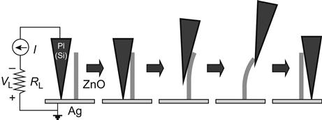
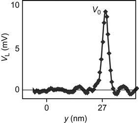
Experimental devices and processes using a conductive AFM tip to bend a piezoelectric nanowire to generate electricity are shown in Figure 7.4. The corresponding voltage signals are shown in Figure 7.5, where y is the bending amplitude of the nanowire from the vertical.