Characterization and Analysis of Nanomaterials
In order to elucidate nanoscale-driven properties, thorough characterization and analysis is required as materials with identical chemical composition can have vastly different properties depending on the size-scale of the material. As such, Chapter 2 is devoted to summarizing many aspects of nanoscale materials characterization and property analysis. Structural and chemical methods will be introduced, along with various microscopy methods. Methods for determining electrical, magnetic, mechanical, thermal, and optical properties will be summarized.
Keywords
Size analysis; structure analysis; nanoscale properties; electron microscopy; atomic force microscopy
Complete characterization and analysis of nanomaterials include particle composition, particle size distributions, morphology/shape, structural analysis, surface characterization, surface area analysis, optical properties, magnetic properties, and others [1].
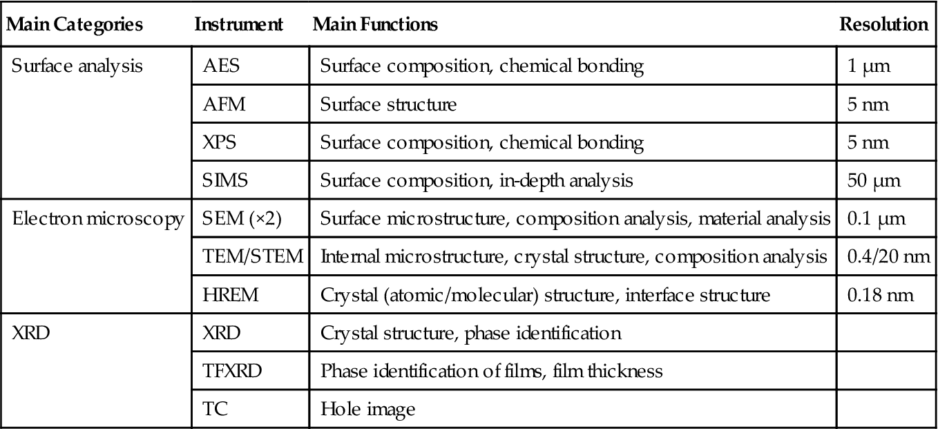
Conventional characterization methods for nanomaterials can vary from system to system but commonly include transmission electron microscopy (TEM), X-ray diffraction (XRD), field-emission scanning electron microscopy (FE-SEM), energy dispersive X-ray spectroscopy (EDS), X-ray photoelectron spectroscopy (XPS), X-ray absorption fine structure (XAFS), inductively coupled plasma mass spectroscopy (ICP-MS), vibrating sample magnetometer (VSM), Auger electron spectroscopy (AES), Mossbauer spectroscopy, and differential scanning calorimetry (DSC), to name a few. For nanoparticles with a size less than 10 nm, different techniques are required, such as high-resolution electron microscopy (HRTEM), Raman spectroscopy, nuclear magnetic resonance (NMR), ultraviolet photoemission spectroscopy (UPS), scanning tunneling electron microscopy (STEM), secondary ion mass spectroscopy, second neutral-atom mass spectroscopy (SNMS), and field-emission scanning transmission electron microscopy (FE-STEM). Table 2.1 highlights characterization techniques used for nanomaterials with the type of information obtained and the resolution of the instruments (TFXRD indicates thin-film XRD and TC indicates texture cradle).
Table 2.1
Comparison of the Performance of Different Testing and Analytical Instruments for Nanomaterials
| Main Categories | Instrument | Main Functions | Resolution |
| Surface analysis | AES | Surface composition, chemical bonding | 1 μm |
| AFM | Surface structure | 5 nm | |
| XPS | Surface composition, chemical bonding | 5 nm | |
| SIMS | Surface composition, in-depth analysis | 50 μm | |
| Electron microscopy | SEM (×2) | Surface microstructure, composition analysis, material analysis | 0.1 μm |
| TEM/STEM | Internal microstructure, crystal structure, composition analysis | 0.4/20 nm | |
| HREM | Crystal (atomic/molecular) structure, interface structure | 0.18 nm | |
| XRD | XRD | Crystal structure, phase identification | |
| TFXRD | Phase identification of films, film thickness | ||
| TC | Hole image |
2.1 Detection and Analysis of Particle Size
First, we need to find a way to define the size of nanomaterials. For spherical nanoparticles, the diameter is defined as the size of the nanoparticle. As for nanomaterials of asymmetric shapes, the following four definitions are usually used: geometric diameter, equivalent diameter, SSA (specific surface area) diameter, and refraction diameter.
Geometric diameter: For particles of any geometric shape, the largest projected area can be converted into a circle of the same size. The diameter of this circle is the geometric diameter of particles.
Equivalent diameter: The size of powder particles can be measured by using the sedimentation method, centrifugal method, mechanical method, or hydraulic method. Homogeneous spherical particles, for example, have the same terminal settling velocity as nanoparticles; their diameter shall have an equivalent diameter of the nanoparticles.
SSA diameter: Using a variety of possible techniques, the SSA of the nanoparticle can be determined. From the surface area, a diameter can be calculated by one of the even spherical particles with the same formula:
Here, ds is the SSA particle size, ![]() is the sample density, V is volume of material tested,
is the sample density, V is volume of material tested, ![]() is the density of the bulk materials, and S is the calculated surface area of the particles.
is the density of the bulk materials, and S is the calculated surface area of the particles.
Refraction diameter: The diameter of the nanoparticle as determined using XRD techniques.
Typically, the calculated diameter will vary depending on the method used, as shown in Table 2.2.
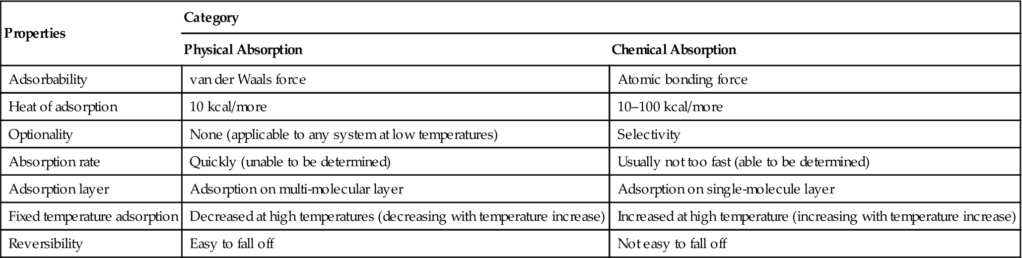
SSA diameter can be measured by using chemical and physical adsorption methods. Physical adsorption and chemical adsorption are compared in Table 2.3.
Table 2.2
Determination of Particle Size
| Size Definition | Determination | Range (μm) | Distribution Benchmark |
| Geometric diameter | Optical microscopy | 500–0.2 | Number distribution |
| Electron microscopy | 10–0.01 | Number distribution | |
| Equivalent diameter | Gravity sedimentation | 50–1 | Mass distribution |
| Centrifugal sedimentation | 10–0.01 | Mass distribution | |
| Gas precipitation | 50–1 | Mass distribution | |
| Proliferation | 0.5–0.001 | Mass distribution | |
| SSA size | Adsorption (gas) | 20–0.001 | Average SSA size |
| Infiltration (gas) | 50–0.2 | Average SSA size | |
| Wetting heat | 12–0.001 | Average SSA size | |
| Refraction diameter | Refraction | 12–0.001 | Volume distribution |
| X-ray line width | 0.05–0.0001 | Volume distribution | |
| X-ray scattering at small-angle | 0.1–0.001 | Volume distribution |
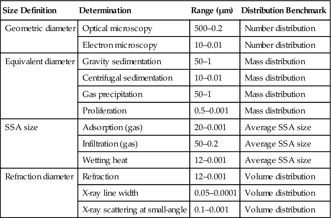
Table 2.3
Comparison of Physical Adsorption and Chemical Adsorption
| Properties | Category | |
| Physical Absorption | Chemical Absorption | |
| Adsorbability | van der Waals force | Atomic bonding force |
| Heat of adsorption | 10 kcal/more | 10–100 kcal/more |
| Optionality | None (applicable to any system at low temperatures) | Selectivity |
| Absorption rate | Quickly (unable to be determined) | Usually not too fast (able to be determined) |
| Adsorption layer | Adsorption on multi-molecular layer | Adsorption on single-molecule layer |
| Fixed temperature adsorption | Decreased at high temperatures (decreasing with temperature increase) | Increased at high temperature (increasing with temperature increase) |
| Reversibility | Easy to fall off | Not easy to fall off |
The BET (Brunauer, Emmett, and Teller) method using multilayer gas adsorption is commonly used for the measurement of SSA materials in the solid phase. It is generally performed using two methods: the volumetric and the gravimetric methods. The volumetric method uses differences in sample volume of a known quantity of gas before and after adsorption to quantify the gas absorbed on the surface. The gravimetric method uses the weight difference of the sample before and after adsorption to determine the amount of adsorbed gas. The gravimetric method is generally considered to be more accurate. Both methods require a high vacuum and rigorous predegassing treatment. The accuracy of the BET method for SSA determination mainly depends on particle shape and defects, such as pores, cracks, and others. These factors may cause a negative deviation of the measured results.
2.2 Detection and Analysis of the Electrical Properties
The electrical properties of nanomaterials can be analyzed by the material’s electric resistance and conductivity, dielectric properties, piezoelectric properties, and surface impedance/volume impedance measurements.
In general, nanomaterials have increased resistance compared to bulk materials; the size scale limits the motion of a large number of electrons through a small crystal size. The more disordered the crystal atoms are arranged, the larger the crystal boundary thickness becomes, thus inhibiting electron mobility. Such an energy barrier on the interface is responsible for the increased resistance. Meanwhile, the relationship between resistance and temperature significantly deviates from those of bulk materials, and some anomalies may even arise, such as in the case of Pd nanomaterials.
Nanomaterials can differ greatly in structure from conventional bulk materials. Their dielectric properties are unique and are mainly represented in the high dependence of the dielectric constant and dielectric loss on particle size. In addition, the electric field frequency may have a strong influence on dielectric behavior. In the materials, the electric displacement and the applied electric field strength E are proportional by a constant known as the dielectric constant ε, with the following relationship: ![]() .
.
Because of the existence of the external electric field, the polarization process may result in electric energy being transferred into heat. Such energy loss is called dielectric loss. Dielectric loss is usually expressed as loss tangent or loss factor tan δ, which is defined as:
Here, ![]() and
and ![]() are the respective real and imaginary parts of the complex dielectric constant
are the respective real and imaginary parts of the complex dielectric constant ![]() .
.
Some materials can separate charge under mechanical action (stress or strain). Such a phenomenon is called the piezoelectric effect. The prefix piezo- comes from Greek, meaning “pressure.” Regarding the mechanism of the piezoelectric effect, Voigt pointed out as early as 1894 that this effect can only be found in crystals formed by the noncentrosymmetric lattice. So far, research of micro-theory on the piezoelectric effect still faces many problems, mainly with inconsistencies with experimental results. Yet researchers have made it clear that the piezoelectric effect is essentially caused by the polarization of crystal medium. Piezoelectric material has electrical response to mechanical stress. Conversely, if this operation can be reversed, that is, by applying a voltage across the material, a mechanism stress of strain occurs. Objects with a piezoelectric effect are known as piezoelectric materials.
Detection and analysis of electrical properties of nanomaterials can be performed by using the following instruments:
1. Digital multimeter (with three functions), which tests AC and DC voltage and current, resistance, and diode.
2. High impedance meter, which tests the nature of electrical insulation.
3. Four-point probe, which tests the material surface resistance.
4. Metal insulator semiconductor component, which measures dielectric constant, threshold voltage, carrier concentration, the thickness of the insulating layer, insulating layer capacitors, and others.
In addition, scanning probe microscopy (SPM) can also be used. At present, SPM has developed into a major technique for the measurement of electrical properties of nanomaterials.
2.3 Detection and Analysis of Magnetic Properties
Magnetic properties of materials are related to the composition, structure, and status of the specific material. Some magnetic properties such as magnetization and susceptibility are closely related to the material’s crystal size, shape, distribution, and defects. Other magnetic properties such as saturation magnetization and Curie temperature are related to the crystal phase and number of materials.
Nanomaterials differ greatly from conventional bulk materials in properties, especially in their magnetic properties. A majority of magnetic properties are different in nanomaterials when compared to the bulk nanoparticles, namely magnetic transformation and superparamagnetism, coercive force, Curie temperature, and susceptibility (see Chapter 5). Here, only a brief introduction is provided.
Néel temperature represents the characteristic temperature (critical temperature) of magnetic properties of certain metals, alloys, and salts. Below this temperature, the material has a spontaneous nonparallel magnetic ordering and displays anti-ferromagnetism; however, above this temperature, the material becomes paramagnetic. Néel temperature Tn is determined by the nearest coordination number of atoms, atomic spacing, as well as the types of nearest neighbor atoms.
Magnetic susceptibility is the ratio of the material magnetization and magnetic field strength. When the two physical quantities are not in the same direction, this ratio is a tensor; when they are in the same direction, the ratio is a simple scalar.
Materials tend to be magnetized under an external magnetic field. To reduce its intensity of magnetization to zero, the reverse magnetic field strength to be applied is called the coercive force. If the size of nanoparticles is larger than the critical size in the superparamagnetic state, then the coercive force will actually increase along with a reduction of the size. There are two interpretations of this phenomenon. One is that the small size makes each particle basically a single magnetic domain, in which nanoparticles behave like a permanent magnet. To reverse the magnetic moment formed by a combination of particle contributions, the reverse magnetic field required will naturally be great. Another interpretation states that due to the magnetostatic effects, spherical nanoparticles may form chains, resulting in an increased coercivity.
The Curie temperature indicates the characteristic temperature (critical temperature) at which a material loses strong magnetism or ferrimagnetism. Above this temperature, the material is paramagnetic. Curie temperature (TC) is one of the major magnetic parameters of materials, and it is related to the atomic structure of a material and its spacing. These phenomena are also the main metrics in assessing magnetic properties of nanomaterials.
Magnetic properties of nanomaterials can be detected by using methods such as magnetic force microscopy (MFM) and NMR.
The MFM is a surface detection technology that involves using magnetic interactions between silicon probes coated with magnetic thin film and using the sample to obtain the surface magnetic structure. In 1987, two scientists, Martin and Wickramasinghe, developed the MFM technology [2]. Initially, only a magnetic image was obtained, whereas the appearance of the structure of materials was not available. At present, MFM is executed through two-step scanning in which intermittent contact scanning is first used to obtain the surface shape of a sample, and then the probe is raised to a certain height for scanning to capture magnetic images. The principle is the same as in noncontact atomic force microscopy (AFM). It has higher resolution (~50 nm) and is easy to use and applicable in various environments. MFM technology has gradually become an important detection technique in magnetic materials research and can be applied to magnetic film, magnetic memory devices, magnetic recording results, and others. Rugar and colleagues designed a magnetic force microscope that used a small bias voltage (1–10 V) that was applied between the probe and the sample to increase the attraction between the tip to improve the stability.
In a strong magnetic field, some nuclei may have split spin energy levels that will be able to absorb electromagnetic waves (i.e., electromagnetic radiation) to produce a resonance phenomenon, called NMR. NMR can be generated under the following conditions: (1) when the nuclear magnetic moment is not zero; (2) when there is a strong and uniform external magnetic field; (3) when there is a specific frequency of electromagnetic waves to be applied to create nuclear resonance.
The NMR method uses nondestructive detection and can be applied to analyze the physical and chemical properties of materials. Compared with the same nondestructive inspection as X-ray detection and infrared detection, NMR has the following advantages: (1) quick detection rate; (2) a specific functional group that can be locked to detect whether there are precursors or byproducts through incomplete reaction, which facilitates the control of the purity of products and finds ways to enable purification and separation; and (3) detection is based on the electromagnetic wave, so it is not subject to the impact of the size, appearance, and color of material samples.
2.4 Detection and Analysis of the Mechanical Properties
Yield strength is defined as the stress at which a material irreversibly deforms. After the stress exceeds this elastic limit, deformation increases rapidly, including elastic and plastic deformation. When the stress reaches a particular value, plastic strain increases dramatically and a small region of fluctuation may occur on the stress–strain curve. This phenomenon is known as yielding. The maximum and minimum stress values at this stage are known as the upper and lower yield points respectively. Because the lower yield point value tends to be more stable, it is defined as the yield point or yield strength. Yield strength is the upper strength limit of a material at which point it can still be safely used. According to the empirical formula by Hall Petch, the yield strength of materials can be expressed as:
Here, ![]() is friction stress, d is the average size of crystals, and
is friction stress, d is the average size of crystals, and ![]() is an empirical constant.
is an empirical constant.
TEM and AFM research has shown that carbon nanotubes have excellent mechanical properties, such as high elastic modulus, high elastic strain, and high rupture strain, which all match those in computational experimentation. Compared with the conventional bulk materials, nanostructured materials commonly double in strength and hardness. Furthermore, nanocomposites have shown dramatic improvements in strength, toughness, abrasion resistance, aging resistance, pressure resistance, compactness, and waterproof properties. Nanoceramic materials pressed from nanoparticles exhibit good toughness and ductility.
2.5 Detection and Analysis of Thermal Properties
Regarding the thermal properties of nanomaterials, physical quantities that require characterization include the thermal conductivity coefficient, specific heat, thermal expansion, thermal stability, and melting point.
As the thin film layer of material reaches a certain thickness, the grain boundary effect will have an increasingly significant impact on the thermal conductivity. Furthermore, the thermal conduction coefficient perpendicular to the film tends to decrease as the film thickness decreases.
Theoretical predictions and experimental results confirmed that nanostructured materials have specific heat values much higher than those of conventional bulk materials. Nanomaterials have a comparatively chaotic distribution of atoms on the structure, which has a higher volume as compared with bulk counterparts. Thus, entropic contributions due to this noncrystalline surface contribute much more to specific heat than the average coarse crystalline materials, leading to increased specific heat.
Nanocrystals are almost twice as large as the average crystals in the thermal expansion coefficient, with the increased t mainly contributed by the composition of the crystalline boundaries. The main instrument for measuring the thermal expansion coefficient of materials is known as a thermal expansion analyzer, but it is also known as a thermal dilatometer analyzer or a thermomechanical analyzer. The analysis of the thermal expansion coefficient of materials can provide an understanding of molecular motion, structural changes, and thermal expansion behavior. To solve problems such as heat bonding of different materials in the manufacture of semiconductor devices, a thermal expansion analyzer is the best tool for the analysis.
Melting point is the temperature at which a material is transferred from solid into liquid. For crystalline objects, there is a clear melting point; however, noncrystalline objects have an ill-defined melting point. The temperature may increase to a value at which a small number of atoms in an overall structure begin to move simultaneously with a liquid-like behavior. This temperature is known as the glass transition temperature (Tg). At temperatures below Tg, the glass material is in a solid state; at temperatures higher than Tg, it is a supercooled liquid. Expressed in mechanical terms, if the temperature is below Tg, then elastic deformation will occur; if the temperature is higher than the Tg, then viscosity (liquid type) deformation begins.
Thermal decomposition temperature is a value at which the material bonds can be heated to a broken state and dissociated into other substances.
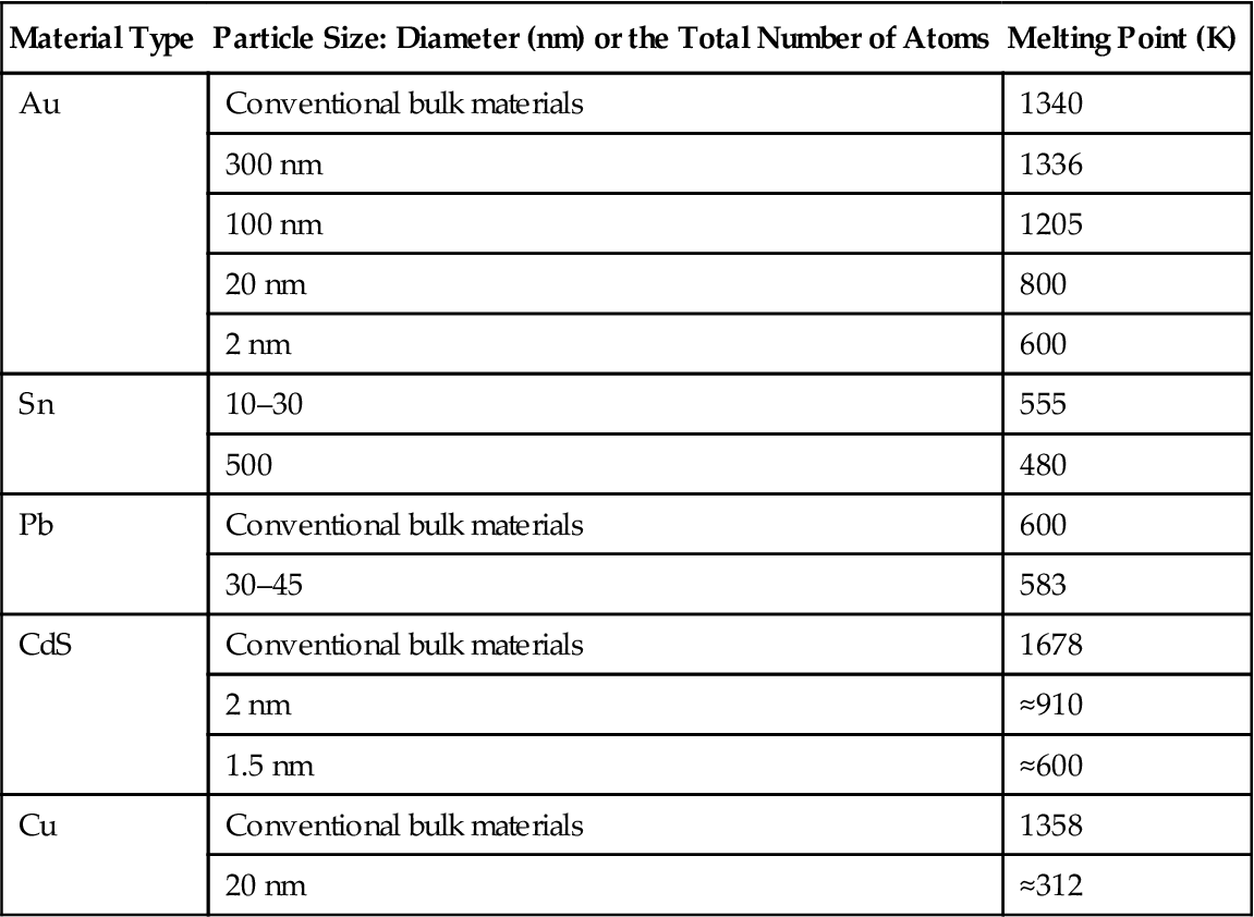
For noncrystalline or amorphous nanomaterials that are plasticized, glass transition temperature and thermal dissociation temperature other than the melting point are also very critical thermal properties. Table 2.4 shows the melting point of several kinds of material at different scales.
Table 2.4
Melting Point of Several Materials at Different Scales
| Material Type | Particle Size: Diameter (nm) or the Total Number of Atoms | Melting Point (K) |
| Au | Conventional bulk materials | 1340 |
| 300 nm | 1336 | |
| 100 nm | 1205 | |
| 20 nm | 800 | |
| 2 nm | 600 | |
| Sn | 10–30 | 555 |
| 500 | 480 | |
| Pb | Conventional bulk materials | 600 |
| 30–45 | 583 | |
| CdS | Conventional bulk materials | 1678 |
| 2 nm | ≈910 | |
| 1.5 nm | ≈600 | |
| Cu | Conventional bulk materials | 1358 |
| 20 nm | ≈312 |
Thermal properties of nanomaterials are usually detected and analyzed by use of thermogravity analysis (TGA) and derivative thermogravimetry (DTG).
TGA can provide continuous measurement based on weight changes of materials in the process of heating during the measurement. Specifically, changes in mass are monitored as a function of temperature at a predetermined temperature rate and can be correlated to mass losses and thermal transitions in the material. Differential treatment can be completed at the same time. Namely, the recording of quality changes constitutes the DTG measurement technique.
By means of TGA (or DTG), a number of thermal properties of materials can be found, for example the aging temperature during pyrolysis and aging dynamics, aging behavior at different temperatures and in different gas environments, IC packaging materials used in the manufacturing process of executable semiconductor devices, flexible printed circuit boards, and glass substrates, ceramic substrates, and other components of analysis.
In the colloidal system, the related thermal properties of particles also include Brownian motion, diffusion and sedimentation balance, among others.
In Brownian motion, the average particle displacement ![]() can be expressed as:
can be expressed as:
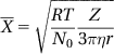
where R is the ideal gas constant, T is the absolute temperature, N0 is the Avogadro constant, Z is the interval of observation time, ![]() is the viscosity of the dispersion medium, and r is the particle radius.
is the viscosity of the dispersion medium, and r is the particle radius.
Brownian motion has significant implications in the nature of colloidal particles. Brownian motion is an important factor that may affect the stability of a dispersion system of colloidal particles. Due to Brownian motion, the sedimentation of colloidal particles occurs not because of gravimetric forces but because of colloidal aggregation caused by interparticle collisions, resulting in sedimentation.
The phenomenon of diffusion is related to mass transfer, which arises from the Brownian motion of particles (Brownian motion) when there is a concentration gradient. The larger the particles and the smaller the thermal velocity, the less apparent the diffusion becomes. In general, the diffusion coefficient is used for measuring the diffusion velocity. It is a physical quantity of a material that indicates the diffusion capacity.
In the colloidal system, the diffusion coefficient D can be expressed as:
Here, R is the ideal gas constant, T is the absolute temperature, N0 is the Avogadro constant, ![]() is the viscosity of the dispersion medium, and r is the particle radius.
is the viscosity of the dispersion medium, and r is the particle radius.
Because diffusion coefficient is correlated with the average displacement, the derived diffusion coefficient D can also be expressed as:
Here, Z is a specific interval of observation time and ![]() is the average particle displacement in Brownian motion. Table 2.5 shows the diffusion coefficient of sol resulting from gold nanoparticles at 291 K.
is the average particle displacement in Brownian motion. Table 2.5 shows the diffusion coefficient of sol resulting from gold nanoparticles at 291 K.
Table 2.5
Diffusion Coefficient of Sol Resulting from Nano-Au Particles at 291 K
| Size of Nano-Au Particles (nm) | Diffusion Coefficient (109 m2/s) |
| 1 | 0.213 |
| 10 | 0.0213 |
| 100 | 0.00213 |
When the particles suspended in fluid show a settling velocity equal to the diffusion speed, the system reaches a state of equilibrium, namely the sedimentation equilibrium. At the sedimentation equilibrium, the concentration of colloidal particles is subject to the Gaussian distribution law.
The Gaussian distribution law for colloidal particles can be expressed as:
Here, n1 and n2 are the concentration of particles at the cross-section at the height of x1 and x2 respectively, R is the ideal gas constant, T is absolute temperature, A is Avogadro’s constant, r is the particle radius, ![]() is the density of colloidal particles,
is the density of colloidal particles, ![]() is the density of the dispersion medium, and g is the acceleration of gravity.
is the density of the dispersion medium, and g is the acceleration of gravity.
2.6 Detection and Analysis of Optical Properties
The main differences in optical properties between nanomaterials and conventional bulk materials can be explained by the following: (1) strong broadband optical absorption of nanoparticles; (2) band shift of optical absorption; (3) the quantum confinement effect; (4) luminescence of nanoparticles; and (5) optical properties of the dispersion system.
1. Strong broadband absorption characteristics of nanoparticles
Nanoparticles have an enhanced absorption of light at various wavelengths within the visible frequency range, whereas the reflectivity is decreased. Nanoparticles of silicon nitride (Si3N4), silicon carbide (SiC), alumina (Al2O3), and other powders have a strong broadband absorption spectrum range of infrared light. Zinc oxide (ZnO), iron oxide (Fe2O3), and titanium dioxide (TiO2) have strong absorption of ultraviolet (UV) light.
2. Frequency shift of optical absorption band
A frequency shift of the optical absorption band of nanoparticles is manifested both on the blue shift and the red shift of absorption spectra, depending on intra- and interparticle environments.
After chemical modification of the surface of semiconductor nanoparticles, their absorption spectra will have a red shift. Quantum size effects or surface effects may be attributed to the blue shift of the absorption band whereas an increased overlap of electron wave functions will lead to a red shift of the absorption band.
3. Quantum confinement effect
When the size of semiconductor nanoparticles is smaller than the Bohr radius aB of an exciton, overlap of the wave functions of the electron and the hole will occur, resulting in an exciton absorption band. The overlapped electron and hole wave functions will increase with the reduction of the size of nanoparticles by ![]() . Exciton absorption is enhanced and shows a blue shift.
. Exciton absorption is enhanced and shows a blue shift.
4. Luminescence of nanoparticles
Silicon with a particle size of less than 6 nm can emit visible light at room temperature. As the particle size decreases, the intensity of the emission band will increase and exhibit a blue shift. Tabagi holds that the luminescence of silicon nanoparticles is a result of the quantum confinement effect of the carriers. Brus believes that because silicon nanoparticles are smaller than 6 nm, the translational symmetry that can only be found in conventional bulk structures will disappear, and therefore the luminous phenomenon occurs.
5. Optical properties of dispersion system
The Tyndal effect of nanoparticles will appear in dispersed systems [3] and is associated with the size of the dispersed particles and the wavelength of light projection.
For characterization of the optical properties of nanomaterials, the commonly used methods include infrared spectroscopy (IR), UV–visible spectroscopy, and scanning near-field optical microscope (SNOM) analysis.
Strictly speaking, in terms of size distribution, IR maps the electronic wave function as a function of depth penetration. Traditional infrared spectrophotometry is classified as the dispersive type and Fourier-transformed infrared spectroscopy (FTIR) is the nondispersive type. FTIR features a larger energy output, very high accuracy and precision in frequency (or wave number) measurement, as well as the feature of multiplicity.
UV–visible spectroscopy is based on the principle of electronic transitions in molecules. Molecular energy includes the electronic state of energy, vibrational energy, and rotation. The unique nature of nanomaterials with different optical absorption properties differentiates them from their bulk counterparts.
SNOM analysis is a combination of SPM and a fiber-optic probe, with the optical measurements and observations available in high spatial resolution beyond the diffraction limit. SNOM combines advantages of optical microscopy and electron microscopy.
SNOM analysis can provide clear optical images of the surface of nanomaterials for spectral analysis and can probe molecular aggregation. Combined with time-resolved fluorescence microscopy, SNOM can also be used to analyze optical phenomena at the nanoscale. At present, near-field optical microscopy has been applied in the fields of biology and medical research, and in research using semiconductor optoelectronic high-density optical media. The resolution of such a technique is ~50 nm.
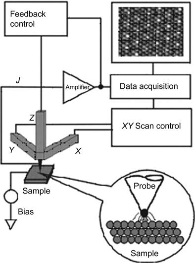
2.7 Scanning Probe Microscopy [4–6]
SPM is extremely advantageous in the study of nanomaterials because atomic-scale resolution of nanomaterial surfaces can be examined. Various surface properties can be explored, including mechanical, magnetic, electrical, thermal, and optical properties. Many researchers have widely applied SPM in their nanotechnology research. The major advantages of SPM include lack of sample preparation and the ability to be used in various environments. Disadvantages are obvious and include low scanning speed, poor data reproduction, and the lack of elemental analysis capabilities. In scanning tunneling microscopy (STM), a small voltage is applied between the metal probe and the conductive samples at a distance between a few and tens of angstroms. Atoms at the probe tip and the sample surface can thus be maintained at a fixed value of tunneling current to measure the shape of the surface structure with atomic resolution. The STM technique can achieve the highest resolution of all known microscopy methods but cannot be used with insulating materials.
2.7.1 Working Principles of Scanning Tunneling Microscopy
The STM uses metal tips to scan the sample surface, which produces a quantum tunneling current under standard operating conditions. Because the tunneling current occurs more strongly on the tip of the atom, STM has atomic-scale lateral resolution. Using tunneling current as measurement signals, the image of the sample surface can be obtained. Therefore, both the sample and probe must be conductive, and the sample surface must be atomically planar for accurate measurements. Such requirements limit the use of STM (Figure 2.1).
2.7.2 Operating Mode of STM
In STM, as the tip scans the surface of the sample, the movement trajectory is recorded. The calculated density distribution from the surface morphology of the sample yields the atomic-scale image of the surface. This method can be used to observe the surface morphology of the sample, with many fluctuations. Meanwhile, the voltage applied in the z-drive is applied to calculate the height value of the surface fluctuations. However, for sample surfaces with little fluctuation, tip height can be controlled to perform a conservation scanning, and the changes in tunneling current are also recorded to obtain the distribution of surface morphology. This scanning mode is highlighted by high speed and the ability to reduce noise and thermal drift on the measurement; however, it is generally not able to be used to observe samples with surface fluctuations larger than 1 nm (Figure 2.2).
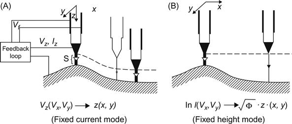
A. Fixed current imaging: The tunneling current (about 1 nA) is set as feedback signals. As the spacing between probe and sample surface is very sensitive to tunneling current, setting the value of the tunneling current means locking the spacing between probe and sample surface. While scanning over the surface of the sample, the probe must adjust its height (i.e., z values) according to the fluctuations of the surface. Therefore, the height variation of the probe can be presented so as to reflect the morphology of the sample surface.
B. Fixed height imaging: Tunneling current values are directly used to present the image. While scanning the sample surface at a fixed height, surface fluctuations will lead to changes in spacing between probe and sample surface, and tunneling current values will also change accordingly (Table 2.6).
Table 2.6
Advantages and Disadvantages of the STM Scanning Modes
| Mode | Principle | Advantages and Disadvantages |
| Fixed current mode | Probe is maintained at a fixed current value height and adjusted with the morphology of the sample surface. The probe height variation is used to present the image of the sample surface. | Advantages: Larger depth of field. Disadvantages: Scan speed is slower and vulnerable to low-frequency noise. |
| Fixed height mode | With the probe being set at a fixed height, tunneling current values are directly used to present changes of surface morphology. | Advantages: Quick scanning rate, which can potentially observe surface dynamics. Disadvantages: Probe damage is possible if large fluctuations in the sample height are present. |
| Current density mode | Combination of the two above-mentioned materials, wherein bias modulation is used to gather images. | Disadvantages: Larger data sets; time consuming. |
2.7.3 STM Application: Atomic Manipulation
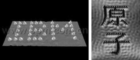
Thirty years ago, a dream of many scientists was the ability to see individual atoms directly and to spatially manipulate individual atoms as desired. Thirty years later, this is no longer a dream, as many laboratories around the world have the knowledge and instrumentation to perform these activities that were once thought to be impossible. In 1990, IBM scientists Eigler and associates performed the first successful manipulation of atoms using an STM scanning needle to move Xe atoms at will on nickel surfaces. To demonstrate their capabilities, they arranged Xe atoms to spell the name of their company, IBM (Figure 2.3). The next year, Hosoki and colleagues, scientists for Japan’s Hitachi Ltd., successfully used small single-atom vacancies to write the word PEACE’91HCRL on the surface of molybdenum disulfide (MoS2). Later, other scientists manipulated nearly 100 iron atoms and formed two Chinese characters “![]() ” (Figure 2.3). These results captured the imagination of the scientific community and were commonly advertised throughout scientific media and conferences at that time.
” (Figure 2.3). These results captured the imagination of the scientific community and were commonly advertised throughout scientific media and conferences at that time.
In fact, there are three ways to manipulate individual atoms on surfaces. The first method is to use the interaction force between atoms on the STM tip and the surface atoms of the sample. Atoms on the surface can be moved from their original location to a specified new location, as demonstrated by Eigler. The second method is to use an electric field to evaporate the surface atom field onto the scan tip, or to manipulate the atoms on the tip and onto the sample surface. This method was used by Hosoki. The third method is to move the atoms with an electric field gradient. This method is currently undergoing thorough investigation and is viewed optimistically by many researchers in the field. The use of STM for atomic surface modification and single-atom manipulation shows wide application possibilities. Currently, it has significant applications in areas such as molecular and quantum devices, information storage, life sciences, and materials sciences. Single-atom manipulation mainly includes three basic steps, namely movement, extraction, and placement. These technologies are also essential for the future application of single-atom manipulation and the surface processing of structures for atomic-scale devices.
The main application of the atomic manipulation technique is in creating nano- or atomic-level structures. One such application is in high-density information storage. IBM scientists have demonstrated the ability in the aforementioned movement of xenon atoms, which can be directly used in the production of atomic-scale high-density memory. If each location without an atom on the surface represents 1 and the location with atoms represents 0, then this surface can be used as binary memory. Such storage density is unprecedented, far exceeding the memory density that is achievable in modern semiconductors and magnetic disks. Furthermore, STM can easily achieve the images of these atoms, which can be thought of as the equivalent to reading bits of data at an atomic level.
2.7.4 Advantages of STM
The scanning tunneling microscope apparatus itself has many advantages that make it a highly effective experimental tool for studying the surface structure of materials and biological samples of microelectronics-related surfaces. For example, STM instruments can be used by biologists in the study of individual protein molecules or DNA molecules, defects in crystals, and structure/morphology studies of microelectronic devices with nanoscale components. Before the invention of STM, the scale could only be potentially observed using destructive methods. STM is a nondestructive method, preserving the sample surface. In addition, STM is not limited to the diffraction limit of optical microscopy, which results in the incapability of imaging objects at half the size of the optical wavelength.
2.8 Atomic Force Microscopy [6,7]
Atomic force microscopy is mainly used in the measurement of atomic van der Waals forces to obtain images of the surface atoms. Because the AFM can observe any material regardless of electrical properties, it has advantages over STM. AFM technology was jointly developed in 1985 by Binnig from IBM and Quate from Stanford University [8] to scan nonconductor materials. The AFM probe, if coupled with a layer of magnetic material, can be used to detect the nanoscale magnetic force as well, known as MFM. If an AFM probe is coupled with a layer of metal, then it is possible to detect electric properties, which is known as static electricity microscopy. Similar approaches can be used to modify the probe for a wide variety of measurements such as near-field optical microscopy and scanning capacitance microscopy. The development of this series is referred to as SPM. Among the series, the atomic force microscope is the most widely used.
2.8.1 Working Principle of AFM
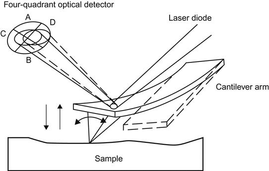
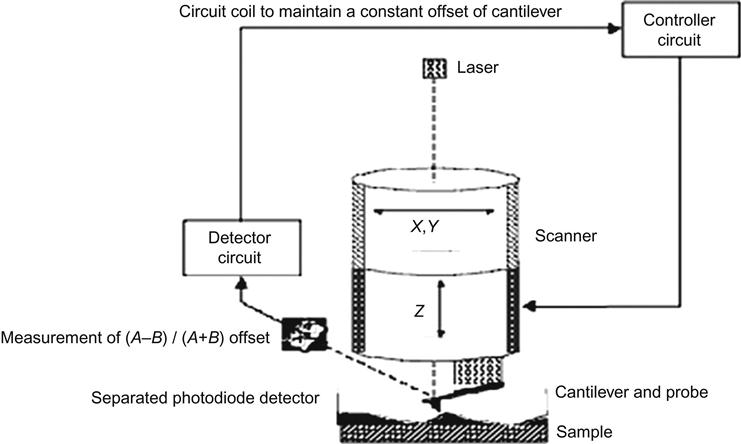
AFM works mainly on the principles of force between the probe and surface atoms, which are recorded by an optical offset to derive images and calculate various parameters. The key component of AFM is a microcantilever, the head of which is designed with a thin, pointed probe used to scan the sample surface. This cantilever is usually made from silicon or silicon nitride, with the curvature of its probe in the nanoscale. Because the probe is placed near the surface of the sample, the bending of the cantilever will comply with Hooke’s law and have an offset as a result of the probe and the interaction with the surface. Typically, the offset can be observed by measuring the reflected laser beam that shoots onto the microcantilever with a light-sensitive diode array. When the probe scans over the sample surface, the laser reflection angle will change, along with the current of the light-sensitive diode. By measuring the current change, the bending or deflection of the cantilever can be calculated. The data will then be analyzed to produce three-dimensional images of the sample surface (Figures 2.4 and 2.5).
2.8.2 Comparison of the AFM Scanning Modes
There are three modes of AFM scanning, namely contact, noncontact, and tapping mode. They are compared in Table 2.7.
Table 2.7
Comparison of the AFM Scanning Modes
| Scanning Mode | Basic Principle | Advantages and Disadvantages |
| Contact (2–3 nm) | In the image scanning, the tip has a gentle contact with the sample surface. A very weak repulsion arises between atoms to produce the probe offset. Feedback is used to control a fixed value. The probe position change is obtained corresponding to all the scanning points, which renders the topographic images of the sample surface. | The contact area is small, but access force may damage the sample, especially for soft materials. However, the larger force can usually get better resolution. Therefore, an appropriate level of force is needed. As the repulsion is very sensitive to the distance, atomic resolution is easier to obtain. |
| Noncontact (<20 nm) | Detection is executed by using the long-range attraction between atoms—van der Waals forces. However, this attraction has a very small rate of change in the distance. Modulation techniques are required to increase the signal to noise ratio. | In the absence of contact between probe and sample, damage is avoided. But under the effects of the water film on the surface of the sample in air, the resolution in general is only 50 nm, while there is the availability of atomic-scale resolution in ultra-high vacuum. |
| Tapping (5 nm) | The probe repeatedly taps on the surface of the sample. As the probe is oscillated to a trough, there is a micro-contact with the sample. Due to the uneven surface of the samples, the atomic force may change the amplitude of the probe in beating. The use of feedback control will be able to obtain a high degree of image. | In the absence of contact between probe and sample, there is no need to worry that the sample may be damaged. But under the effects of the water film on the surface of the sample in air, the resolution in general is only 50 nm, while there is the availability of atomic-scale resolution in ultra-high vacuum. |
2.8.3 Application Examples of AFM
There are a wide range of AFM applications. One such example is in life sciences [9]. Because the AFM works in a very wide scope, direct imaging of biomedical samples can be made in the natural state (air or liquid) with high resolution. Thus, AFM has become a vital tool for studying biomedical samples and biological macromolecules. Applications of AFM in biology include three aspects: morphological observations on biological cell surfaces; observation and study of the structure of biological macromolecules and other properties; and power spectrum curves observed between biological molecules.
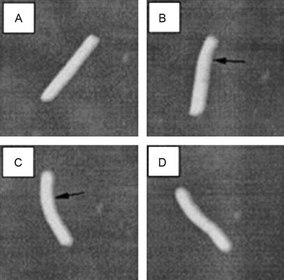
Images here show experiments in which the AFM tip was used in the bending and rotational movement of virus particles (Figure 2.6).