
Basic Properties of Nanomaterials
Nanotechnology, the study of materials and phenomena at the sub-100-nm scale, is an established multidisciplinary field of science with emerging real-world impacts. Applications of nanotechnology are plentiful, including (but not limited to) drug delivery, energy storage, energy harvesting, optics, electronics, optoelectronics, catalysis, tissue engineering, structural materials, and sensing. Chapter 1 provides a brief history and overview of the field of nanotechnology, while also summarizing important property changes observed in nanoscale materials as compared to their bulk counterparts.
Keywords
Nanoscale properties; physical principles of nanomaterials; quantum effects
In 1959, US physicist Richard Feynman, the famous Nobel Prize winner, first proposed the concept of “nanomaterials.” Since then, Feynman’s prediction has gradually become a reality in the development of nanoscience and nanotechnology. Peculiar physical properties of nanomaterials have a significant impact on people’s lives and social development. Nanomaterials began to exhibit an increasing number of applications in sectors such as medicine, home appliances, computers and electronics, environmental protection, textile industry, machinery industry, and others.
1.1 The Nanometer and Its Brief History, Nanoscience, and Nanotechnology
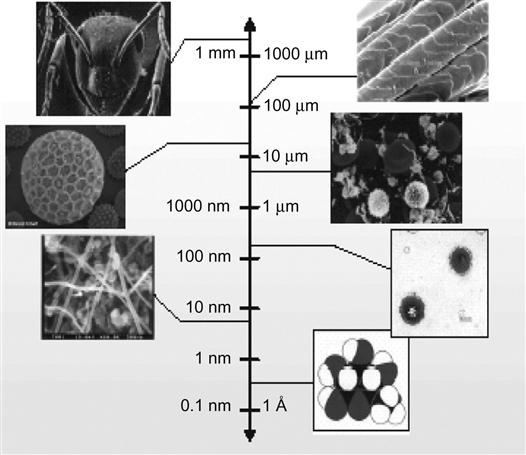
Nano is the metric unit of the nanometer (nm) via transliteration. Like the millimeter and micron, the nanometer is defined as a scale of length, having no special physical meaning. Specifically, it is equivalent to one billionth of one meter (i.e., 1 nm=10−9 m). One nanometer introduces a length of approximately two to three metal atoms being arranged together, or a “width” of 10 hydrogen atoms being arranged alone. A typical virus has a diameter of approximately 60–250 nm, a red blood cell has a diameter of approximately 2,000 nm, and the diameter of a hair is 30,000–50,000 nm (Figure 1.1).
Materials prefixed with “nano” can be traced back to the 1980s; it was used to define particles within a range of 1–100 nm. In July 1990, the first session of the International Symposium on Nanoscience and Nanotechnology was held in Baltimore, MD, and formally announced to the world the science of nanomaterials as a novel branch of materials science. Subsequently, a large number of scientific and technological personnel became engaged in the field of nanotechnology research, and this soon led to a “nano boom” worldwide.
In 1962, Kubo developed the quantum confinement theory on ultrafine particles, which promoted the exploration of nanoparticles in experimental physics. In 1984, the German Professor H. Gleiter and colleagues synthesized nanocrystals such as Pd, Fe, and others. In 1987, Dr. Siegel in the US-based Argonne National Laboratory prepared the nano-TiO2 polycrystalline ceramics, which show good toughness, without any bending fracture under temperature conditions of 100°C or higher. This breakthrough brought about the first worldwide boom in nanotechnology, officially making it a branch of materials science.
As one of the most common elements in nature, the unique bonding orbital of carbon forms an abundant carbon family. People used to believe there were only three carbon allotropes in nature: diamond, graphite, and amorphous carbon. In 1985, Kroto and colleagues found the cage-like C60 molecules with a magic number of 60, in which 60 carbon atoms are respectively located at the top of football-shaped polyhedrons composed of 20 hexagons and 15 pentagons. By using the arc discharge of graphite electrodes, Kratschmer obtained a macro-amount of synthetic C60 for the very first time, triggering another wave of nanotechnology research. The later findings were a large family of spherical and spheroidal carbon allotropes.
In 1991, Professor Iljima from Japan’s NEC Corporation found a hollow tube in the cathode rod with deposition of carbon black as a result of DC arc discharge in an Ar atmosphere. Under the transmission electron microscope, he found that this hollow tube had a diameter of one nanometer to tens of nanometers, and a length of tens of nanometers to one millimeter. Dozens of these tubes are structured together coaxially, leaving a radial spacing of approximately 0.34 nm between the adjacent hollow tubes, for example the plane spacing of graphite (002). This is what is now referred to as the carbon nanotube. Its unique molecular structure of a one-dimensional tube has opened a novel field in the study of one-dimensional nanomaterials. The discovery of carbon nanotubes led to another peak of nanotechnology study.
At present, nanoresearch involves three main areas: nanodevices, nanomaterials, and nanotechnology detection and characterization. The scientific significance of the research on nanostructure and nanomaterials is that it has opened a novel level of people’s understanding of nature, and the subject itself has turned out to be a golden source of knowledge innovation. Nanoscale structural units (1–100 nm) are equivalent to many of the featured lengths in the substances, such as the de Broglie wavelength of electrons, the superconducting coherence length, the thickness of tunneling barriers, and the critical size of magnetic iron, thus making nanomaterials and nanostructures not only different from the microscopic atoms and molecules but also different from the macro-objects in terms of their physical and chemical properties. People’s scope of exploring the nature and creating knowledge has been extended to a middle area between the macro- and micro-objects. In the field of nanotechnology, discovering novel phenomena, understanding novel laws, and developing novel concepts and theories, such activities will lay a foundation for building a scientific framework for nanomaterials. Furthermore, this also will greatly enrich the connotation of the study of nanophysics, nanochemistry, and other novel areas.
Nanotechnology renders human a mode of production and work on the nanometer scale, as well as novel tools and skills distinctively different from those in the traditional sense. For example, if we want to build robots that can enter the blood vessels, then we need to make them very small, so tools used by such robots must be made with nanomaterials. Recently, scientists have invented nanoshovels and nanospoons, which can be used by a vascular robot for operations in blood vessels. This is a typical example of nanotools.
Nanotechnology covers a wide range of contents, such as the following: the manufacturing technology of nanomaterials; the technologies of nanomaterials applied to various fields (including but not limited to high-tech fields); any device that is built in a nanoscope for double-cutting and operation of atoms and molecules; the understanding of new laws of the material transfer and energy transfer within the nanoscope; and others. So, we should not think that nanotechnology merely refers to nanomaterials, or that nanomaterials merely refer to nanopowder. Nanomaterials actually include nanofilaments, nanotubes, nanowires, nanocables, nanothin film, the three-dimensional nanoblock, composite materials, and other materials besides nanopowder. In addition, nanomaterials can be either solid or liquid. For example, there is such a thing called nanowater, which contains smaller clusters of water molecules after being processed by high-frequency ultrasound.
1.2 Characteristics of Nanomaterials
1.2.1 Perfect Law of Nanomaterials
In 1959, Feynman assumed the following: “Imagine that if one day, atoms and molecules could be arranged as what people want them to be, how different the world might be! There is no doubt that if we could control things on the very tiny scale, the scope of physical properties we can get can be greatly expanded.” Now it is known that, in fact, people cannot organize atoms and molecules truly at will to form nanostructured materials, because their formation requires some special laws to be satisfied, such as the so-called perfect law of nanomaterials.
Atomic and electronic structures are commonly used to describe the structure of materials. The main parameters for atomic structure are the lattice constant, bond length, and bond angle, whereas the electronic structure has the energy band, quantum state, and distribution function as its main parameters. These parameters are constants determined for the macrosystem we are familiar with. But for the nanosystem, the majority of parameters may change as the atomic number changes. This is a typical characteristic found in materials and devices in nanotechnology that determines the diversity of nanomaterials. For the nanosystem there is an important law, and we call it the perfect law of nanomaterials. This can be expressed in simple language: “Existence is perfect, and only the perfect can be existent.” It includes a magic number rule of nanocrystals; that is, atom clusters with the atomic numbers of 13, 55, 147, and others are considered to be stable. For example, carbon 60 and carbon 70 have the largest probability of existence in the fullerene structure, whereas structural systems such as carbon 59 or carbon 71 do not exist. That is why Smalley and colleagues [1] discovered that carbon 60 and carbon 70 exist in a number of fullerene structures and thus won the Nobel Prize. For one-dimensional nanostructures, including nanotubes and nanowires, similar rules also apply. The one-dimensional structure can be regarded as constituted by the shells, and each of the shells contains a more sophisticated structure known as a unit, and each unit is an atomic chain. The structure with the center containing one unit and the parcel layer containing seven units is expressed as the 7-1 structure. If the structure also has a shell layer packaged with 11 units beyond it, then it is expressed as the 11-7-1 structure, and so on. The 7-1 and 11-7-1 were only regarded as the most stable structures; this is called the magic number rule for the one-dimensional structure. A two-dimensional membrane is found to obey the defects melting rule; that is, it does not allow the existence of many defects. Once the defects reach a critical number, more defects will arise spontaneously and will completely destroy the two-dimensional crystalline structure. Such characteristics of low-dimensional structures are the specific interpretation of the Perfect Law.
1.2.2 Nano-Effect [2–4]
As materials are reduced to the nanometer scale—within the range of approximately 1–100 nm—the properties of the material may change abruptly so that the material may have some exceptional properties. Materials with such special properties that differ from both the original atomic or molecular components and the macroscopic material are called nanomaterials. Note that if the scale of the materials is within the nanometer range but they do not present special properties, then such materials cannot be called nanomaterials. People used to pay attention only to the microscopic objects like atoms or molecules, or to the macroscopic objects like the universe, and often overlooked this middle scope in between. Actually, a lot of materials exist within this scope in nature, except that we have never noticed the properties of physical objects of this scale before. It was Japanese scientists who took the initiative to gain a true reorganization of the performance of objects within this scale and introduced the concept of nanotechnology. In the 1970s, they successfully prepared advanced micro-ions by using the evaporation method and studied their performance. They found that metals such as copper and silver with electrical and thermal conductivities, after being reduced to the nanoscale, will lose their original nature and become nonconductive and nonthermal.
The same is true for magnetic materials, for example iron–cobalt alloy. When this alloy is prepared with a size of approximately 20–30 nm, the magnetic domain is changed to a single magnetic domain, exhibiting a coercivity 1,000 times higher than the original. In terms of magnetic susceptibility, nanomagnetic metal is 20 times more effective than that of ordinary metals. Its saturation magnetic moment is half that of ordinary metal. When a layer in multilayer film gets its thickness to nanosize, a giant magneto-resistive effect may occur.
Typically, PbTiO3, BaTiO3, and SrTiO3 are ferroelectrics and can become paraelectrics when their size is reduced to nanoscale. Nanosilicon nitride ceramics are characterized by not having a typical covalent bond and being partially polarized on the interface bond with a small AC resistance. Nanoparticles prepared using inert platinum metals (platinum black) can become catalysts with excellent activity.
Changes in body surface area make the sensitivity of nanomaterials much higher than that of volume materials. Nano-optical material has unusual absorptive capacity, and nanometal presents a significantly decreased light reflection capacity: all these features are attributable to the small size and surface effects that give nanoparticles an extremely strong ability to absorb light.
Self-diffusion of Cu nanocrystals is 1016- to 1019-fold that of traditional crystals and is 103 times more than the spread of the crystal boundary. The specific heat of nano-Cu is twice that of traditional copper. The Pd thermal expansion rate of a nanosolid is double that of a normal solid. As a heat exchanger of dilution refrigeration fluid, Ag nanocrystals can be 30% more efficient than those of traditional materials.
When crystals are reduced to nanosize, the dislocation slip is limited to the border and shows hardness that is much higher than that of volume materials. As nanocrystals, copper may have five times stronger hardness than that of the micron-scale. The fracture strength of nano-Fe crystals (6 nm) can be increased 12 times more than polycrystalline Fe.
The following is a more detailed description of nanomaterials in regard to their special nature in the optical, thermal, magnetic, mechanical, and electrical aspects.
1.2.2.1 Exceptional Optical Properties
It has long been known that scale changes of materials come with changes in color. For example, the CaSe powder in larger particles presents a red color, whereas smaller particles of CaSe powder are yellow (Figure 1.2).

When gold was differentiated down to a size less than that of light wavelengths, it would lose its original rich luster and present a black color. In fact, all the metals in the state of being ultrafine particles are shown as black. The smaller the size, the darker the color. Silver–white platinum changes into a platinum black; the metal chrome changes into a chrome black.
Ultrafine particles of metal have a very low rate of light reflection, usually less than l%. At a thickness of approximately a few microns, light can be completely eliminated. This feature can be used for highly efficient transformation of solar energy for heat and electricity and may also be used in infrared-sensitive devices or infrared stealth technology. The Gulf War happened in the spring of 1991, and the coated materials used on the US F-117A stealth fighter contained a variety of nano-ultrafine particles, which have a strong ability to absorb electromagnetic waves of different bands. It can deceive radar to cloak the planes. The United States successfully used these fighter jets in striking important military targets in Iraq.
1.2.2.2 Exceptional Thermal Properties
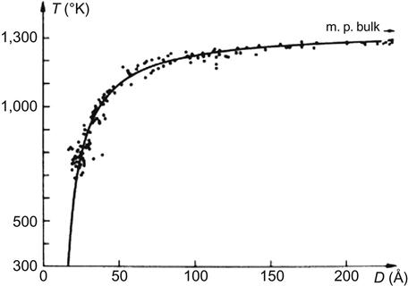
A solid substance has a fixed melting point at its patterns in larger sizes, whereas this point would be significantly reduced in ultrafine forms. When particles are less than 10 nano-orders of magnitude, such decreases are particularly significant.
For example, the conventional melting point of gold is 1,064°C. When its particle size is reduced to 10 nm, the melting point will be 27°C; when the size is reduced to 2 nm, the melting point is only approximately 327°C. The conventional melting point of silver is 670°C, but that of its ultrafine particles can be less than 100°C (Figure 1.3). Therefore, the conductive paste prepared from ultrafine silver powder can be sintered at low temperatures. At this temperature level, the device substrate does not have to be high-temperature ceramic materials; instead, we can use more common materials or even plastic.
Atoms on the surface of metal nanoparticles are quite active. Powder of nanoparticles can be used as solid rocket fuel or catalyst. For example, adding l% of aluminum or nickel ultrafine particles in rocket fuel (weight ratio) can double the combustion heat.
1.2.2.3 Exceptional Magnetic Properties
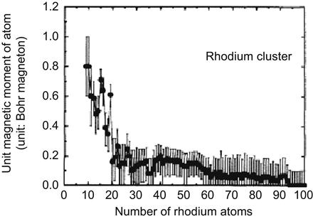
When some materials are changed from bulk to nanoscale, great changes may take place regarding their magnetic properties. Rhodium is a typical example in this respect. We can verify this by increasing the number of rhodium atoms in Rh clusters (Figure 1.4).
When the particle size is reduced to ![]() μm, its coercivity shows a 1,000-fold increase. However, if its size is further reduced to less than approximately
μm, its coercivity shows a 1,000-fold increase. However, if its size is further reduced to less than approximately ![]() μm, the coercive force will conversely reduce to zero, presenting a surplus paramagnetic nature.
μm, the coercive force will conversely reduce to zero, presenting a surplus paramagnetic nature.
Magnetic properties of ultrafine particles with high coercivity can be used for the production of recording magnetic powder with high-density storage, which is currently used in the manufacture of tapes, disks, and magnetic cards in considerable volume. Based on the superparamagnetic feature, ultrafine magnetic particles can be used to prepare magnetic fluids that can be used for a wide range of purposes.
1.2.2.4 Exceptional Mechanical Properties
Nanomaterial particles have a very small size and have a good surface effect. One gram of nanomaterial can form a surface area of up to several hundred square meters. Products prepared using nanotechnology have superior strength, flexibility, and scalability. We can understand this by looking at a caterpillar with thousands of pairs of feet. When it is adsorbed on a smooth glass surface, its large contact area can even resist a level 12 typhoon.
Ceramic materials are usually very brittle, and a ceramic pot can be easily broken when something is thrown at it. However, nanoceramic material prepared by nano-ultrafine particles can have the same good tenacity as a spring.
Studies have shown that high intensity of people’s teeth is due to their structure made of nanomaterials, such as calcium phosphate and others. Metal nanocrystals are as hard as three to five times that of the traditional metals of coarse grains. As for composite nanomaterials (such as metal–ceramic), their application is very broad.
1.2.2.5 Exceptional Electrical Properties
In the scope of nanomaterials, the electronic movement is restricted inside nanoparticles; as a result, quantization of electron energy occurs. Thus, we can prepare special metal particles that can be conductive under a certain voltage and nonconductive under other voltages. Metals used as conductors such as copper will lose their conductivity as their size is reduced to a few nanometers, whereas insulation materials like silicon dioxide will lose their insulating properties and become conductive.
There is also a strange phenomenon in that when a metal nanoparticle acquires an additional electron from the external circuit, it shows negative electricity. The Coulomb force of the electron is strong enough to exclude the next electron from having access to the metal particle from the external circuit, thus cutting off the continuity of current. This is the so-called Coulomb blocking effect. The Coulomb blocking effect inspires people to think about whether we can develop a master electronic device that is controlled by a single electron—the so-called single-electron device. Single-electron devices can be small enough to be integrated to make computer chips with capacity and computing speed many times that of the currently used chips.
1.2.3 Natural Nano-Effect
Nanomaterials are usually man-made synthetic materials, but there are many nanomaterials in nature that also demonstrate some peculiar properties. For example, note that some plant leaves, despite dirt in their environment, can remain clean. Over the years, people have found that such a feature involves hydrophobic materials on the rough surface and the outermost lower waxy surface arranged by nano-order (100–200 nm) rules. The nanorough surface is the primary factor in the mechanism that protects the leaves from dirt. Even when the leaves are covered by pollutants, their surface can be easily washed clean with water. We call this the self-cleaning effect, or lotus effect.
Nanometer-sized cilia exist on the surface of lotus leaves. Under an electron microscope, we can see that cilia form bulges on the surface of its leaves. This prevents the leaves from becoming easily adhesive to water and sludge particles, and that is why lotus leaves show an obvious effect of self-cleaning. Technically speaking, the surface of a lotus leaf is structured with villi that can strengthen its hydrophobic ability. The so-called hydrophobic effect refers to the fact that the surface of an object has a weak force with water molecules and it is difficult for it to absorb water molecules.
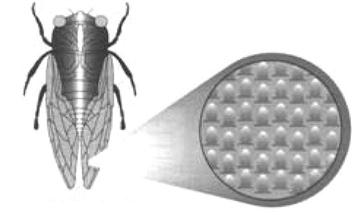
The self-cleaning effect of insects is similar to this. Insects need to maintain a balance of their bodies when they are flying. If their wings carry some dirt, then the weight can cause imbalances and incur flight problems. So, insects have to clean their wings from time to time. Insects with large-scale wings cannot clean their wings with legs, but because the surface of the wings of most insects has a nanostructure, they can be self-cleaning (Figures 1.5–1.7).
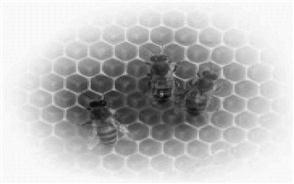
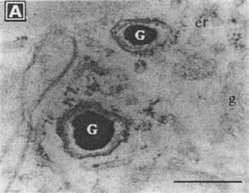
It was found that pigeons, dolphins, butterflies, bees, water magnetotactic bacteria, and other organisms have magnetic ultrafine particles within their bodies that enable this type of organism to navigate under a geomagnetic field. Magnetic ultrafine particles in the bodies of bees (G in Figure 1.8) are essentially a biological magnetic compass that can accurately position the geomagnetic field and determine the magnetic declination and magnetic inclination; it is the flight navigation system of bees. Studies through electron microscopy have shown that magnetotactic bacteria living in water usually contain magnetic oxide particles with a diameter of approximately ![]() μm. By virtue of these particles, magnetotactic bacteria can swim down to the nutrient-rich underwater world.
μm. By virtue of these particles, magnetotactic bacteria can swim down to the nutrient-rich underwater world.
1.3 Physical Principles of the Nano-Effect
As mentioned, nanomaterials are different from the macro-objects in physical and chemical properties, as well as from the microscopic atoms and molecules. When material components reach nanoscale, nanomaterials will show a nature very different from that of volume materials. Nanomaterials can have unique characteristics that are brought about when the scale of a phase on a dimension in the composition of a material is reduced to nanoscale. At the nanometer scale, atomic and molecular interactions may strongly influence macroscopic properties of materials, resulting in changes in mechanical, electrical, and optical properties. Basically, the characteristics of nanomaterials are small size effect, surface interface effect, quantum size effect, quantum tunneling effect, and others [5–8]. These basic features can be explained qualitatively using the theory of Kubo and colleagues.
1.3.1 Discontinuity of Electron Levels
The band theory suggests that a single atom has discrete energy levels. With an increase in the number of atoms in solids (conduction electron number N), atomic levels may change into a discrete band (Figure 1.9). Macroscopic objects contain an unlimited number of atoms; that is, for the number of electrons N conductivity tends to infinity, and large particles or macroscopic objects may have a gap between the macrolevels that come close to zero. Therefore, at high temperature or with overall size, electrons near the Fermi level of metals are generally at a continuous level.
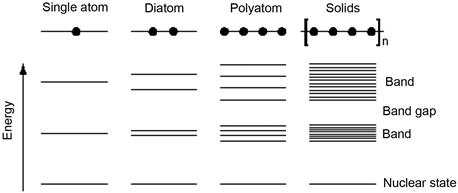
Regarding the nanoparticles containing a limited number of atoms, the value of N is quite small. This leads to a finite energy gap value, which means the energy levels are discrete at low temperatures. As a result of the energy level spacing being greater than thermal energy, magnetic energy, static magnetic energy, electrostatic energy, photon energy, or the concentration energy in the superconducting state, the nanoparticles will significantly vary with respect to their magnetic, optical, sound, heat, electricity, superconductivity, and macrocharacteristics.
1.3.2 Kubo Theory
Nanoparticle size is very small and contains very few atoms, thus its mass is minimal. Many phenomena cannot be explained with the nature of bulk matter that usually contains an unlimited number of atoms. This special phenomenon is usually referred to as a volume effect. One of the well-known theories is the Kubo theory, which is a typical example of the volume effect.
The Kubo theory refers to the state distribution of electron energy levels near the Fermi surface of metallic ultrafine particles. When particles enter the nanosize, the quantum size effect would trigger the quasi-discrete phenomena on continuous energy levels of the original bulk metal. At the beginning, electronic energy levels around the Fermi surface of a single small particle at low temperatures were regarded as the energy levels of the same spacing. A Fermi surface here refers to the equal energy surface with energy as εF in the space k at the temperature of absolute zero. The Fermi surface functions as a separator between the electronic orbits that are filled and not filled.
The specific heat of a single ultrafine particle can be expressed as the following equation:
![]() is level spacing,
is level spacing, ![]() is the Boltzmann constant, and T is absolute temperature.
is the Boltzmann constant, and T is absolute temperature.
At high temperatures, ![]() ,
, ![]() ; that is, the specific heat is independent of temperature, which is consistent with that of the bulk metals. However, at low temperatures (
; that is, the specific heat is independent of temperature, which is consistent with that of the bulk metals. However, at low temperatures (![]() ),
), ![]() ,
, ![]() , which is totally different from bulk metals, because the specific heat and temperature are in a relationship as
, which is totally different from bulk metals, because the specific heat and temperature are in a relationship as ![]() .
.
Although the approximate model for the equal energy level is used to derive the specific heat formula of a single ultrafine particle at low temperatures, this practically cannot be confirmed by experiments because we can perform experiments only on a collection of ultrafine particles. Kubo made an outstanding contribution regarding the use of a novel theory with ultrafine particles to find a solution to the difficulties in consistency between theory and experiment. Kubo made two key assumptions of the electronic states of large aggregates of small particles.
1.3.2.1 Hypothesis Regarding Degenerate Fermi Liquid
Kubo took the electronic state of ultrafine particles near the Fermi surface as degenerate electronic gas under size restrictions and further assumed their energy levels as discrete energy levels of the quasi-particle state, while the interaction between quasi-particles can be neglected. As ![]() (
(![]() indicates the average energy level spacing between the two adjacent levels), the distribution of electronic energy levels in such a system near the Fermi surface follows a Poisson distribution.
indicates the average energy level spacing between the two adjacent levels), the distribution of electronic energy levels in such a system near the Fermi surface follows a Poisson distribution.
Here, ![]() is the spacing between two levels,
is the spacing between two levels, ![]() is the probability density of the corresponding
is the probability density of the corresponding ![]() , and n is the number of energy levels between these two energy states. If
, and n is the number of energy levels between these two energy states. If ![]() is the spacing between adjacent energy levels, then n=0. Kubo and colleagues pointed out that the probability
is the spacing between adjacent energy levels, then n=0. Kubo and colleagues pointed out that the probability ![]() of finding two energy states with a spacing of
of finding two energy states with a spacing of ![]() is relevant to the nature of Hamiltonian transformation. For example, under the conditions of weak interaction of spinning and the orbital (note that the spinning–orbital interaction will enable the energy levels of all atoms with a valence electron to be split into two levels) and a small external magnetic field, the electronic Hamiltonian occurs with the space–time inversion invariance. In the case of
is relevant to the nature of Hamiltonian transformation. For example, under the conditions of weak interaction of spinning and the orbital (note that the spinning–orbital interaction will enable the energy levels of all atoms with a valence electron to be split into two levels) and a small external magnetic field, the electronic Hamiltonian occurs with the space–time inversion invariance. In the case of ![]() being relatively small,
being relatively small, ![]() decreases as
decreases as ![]() decreases. Obviously, Kubo’s model is superior to that of equal energy level spacing, because it reasonably explains physical characteristics of ultrafine particles at low temperatures.
decreases. Obviously, Kubo’s model is superior to that of equal energy level spacing, because it reasonably explains physical characteristics of ultrafine particles at low temperatures.
1.3.2.2 Electrically Neutral Assumption of Ultrafine Particles
Kubo believed that it was rather difficult for an electron to be removed or placed in an ultrafine particle. He proposed the following well-known formula:
In this equation, W is the power made to overcome the Coulomb force for an electron removed from or placed in an ultrafine particle, d is the diameter of the ultrafine particle, and e is the electronic charge. This formula shows that, with the decrease of d values, W increases. Therefore, thermal changes at low temperatures make it very difficult to change the electron-neutrality of ultrafine particles. It is estimated that at temperatures that are low enough, a particle size of 1 nm might have W two orders of magnitude smaller than ![]() . According to Eq. (1.2), we know that
. According to Eq. (1.2), we know that ![]() . Small particles of 1 nm showed a highly obvious quantum size at low temperatures.
. Small particles of 1 nm showed a highly obvious quantum size at low temperatures.
Kubo and colleagues proposed the relationship of the spacing between adjacent electronic levels and the particle diameter with the following well-known formula:
Here, N is the total number of conductive electrons in an ultrafine particle, V is the volume of the ultrafine particle, and EF is Fermi level. It can be expressed as follows:
Here, n1 represents the electron density and m represents equality. In Eq. (1.3), it can be seen that when the particle is spherical, if the particle diameter is expressed by d, then
that is, with the decrease of the particle size, the energy level spacing increases. Clearly, when the particles change into bulk pieces, the volume tends to infinity, and then ![]() , in conformity with band theory.
, in conformity with band theory.
1.3.3 Quantum Size Effect
Material is inversely proportional in level spacing to the atomic number N. Therefore, when the particle size is reduced to a certain extent, with the particle containing a finite number of atoms N, the electronic energy levels near the Fermi level of nanometal will change from the quasi-continuous state into a discrete state. For semiconductor nanoparticles, there are noncontinuous molecular orbitals that are occupied at the highest level and unoccupied at the lowest level, along with a widened energy gap. When the energy gap spacing is greater than material properties such as thermal energy, magnetic energy, electrostatic energy, photon energy, and others, it may lead to distinctively different properties than those of macromaterials. This phenomenon of a widened energy gap is known as the quantum size effect.
Nanoparticles contain a finite number of atoms, and the total number of electronic conductivity (N) has a very small value. This leads to a certain value of δ, which means a split-level space. When the energy level spacing is greater than thermal energy, magnetic energy, static energy, photon energy, or the pool of the superconducting state, the quantum size effect should be taken into consideration.
At 1 K, for example, different particle sizes may cause Ag to be either a conductor or an insulator. We can calculate the critical size for such a change as follows.
From ![]() and
and ![]() , we get
, we get
When T=1 K, the minimum level spacing is ![]() , which when incorporated into the aforementioned formula gives
, which when incorporated into the aforementioned formula gives ![]() . According to the Kubo theory, only when
. According to the Kubo theory, only when ![]() will the split level occur, thus giving rise to the quantum size effect; that is,
will the split level occur, thus giving rise to the quantum size effect; that is,
We can see that as the particle diameter ![]() , Ag of nanoparticles turns into a nonmetallic insulator. If the temperature is higher than 1 K, then the requirement
, Ag of nanoparticles turns into a nonmetallic insulator. If the temperature is higher than 1 K, then the requirement ![]() must be satisfied to be able to become an insulator. It should be noted here that in the actual situation, the metal insulator change requires meeting the conditions of both
must be satisfied to be able to become an insulator. It should be noted here that in the actual situation, the metal insulator change requires meeting the conditions of both ![]() and e-life
and e-life ![]() . Experiments found that nano-Ag does have very high resistance, similar to that of an insulator, which means that nano-Ag meets the preceding two conditions.
. Experiments found that nano-Ag does have very high resistance, similar to that of an insulator, which means that nano-Ag meets the preceding two conditions.
The problem of materials from the ultraviolet to the visible light range has always been a hot topic. The light emission we are referring to is approximately associated with the microprocess of radiative electron transition. Nanostructured materials have very small particles and that small size will lead to the quantum confinement effect. With the disorder of interfacial structure, it is easy to form excitons, particularly surface excitons. The interface may occupy a larger size, with the existence of many defects in the interface, such as hanging bonds, unsaturated bonds, and impurities. This may have many additional energy gaps in the energy gap. Because of the shifting cycle being damaged in nanostructured materials, rules for choice of electronic transitions in the conventional materials of momentum space are not likely to apply to nanomaterials. These will lead to nanostructured materials being different from conventional materials regarding light emission and having their own characteristics instead.
1.3.4 Small Size Effect
When the ultrafine particle size is smaller than the wavelength of light, the length of magnetic exchange, the width of magnetic domain wall, the de Broglie wavelength of conduction electrons as well as the correlation length or the perspective depth of the superconducting state and other physical characteristics or even less periodic boundary conditions of crystals will be destroyed. At the same time, near the particle surface layer of amorphous nanoparticles, the atomic density reduces and physical properties also show a novel effect, such as changes from magnetic order to magnetic disorder, changes in magnetic coercivity, and decrease in metal melting point. This has led to a novel small size effect that can be found in sound, light, electricity, magnetic, mechanical, and other characteristics, such as a significant increase in light absorption accompanying the plasmon resonance absorption peaks, changing from an ordered magnetic state to the disordered state, superconducting phase changing to the normal phase, changes in phonon spectrum, and so on.
Nanoparticles with small size effect have opened some novel areas of technology application. For example, strong magnetic particles in nanoscale (Fe–Co alloy, iron oxide, and others) can be used in the manufacture of magnetic cards, magnetic keys, magnetic tickets, and magnetic fluids. Among these, magnetic fluid has important applications in electro-acoustic devices, damping devices, rotary seals, and lubrication. Nanoparticles can have melting points well below those of bulk metals and can provide novel technology for the powder metallurgy industry. The nature of plasmon resonance frequency changing with the size can be used in combination with controlled displacement of the absorption edge for the manufacture of nanomaterials of microwave absorption of a certain bandwidth.
The optical properties of a material depend on its reflective properties or the performance of absorbing sunlight. For example, if a leaf is green, then it means that it absorbs other wavelengths of light while reflecting the wave of the green. Red pigment indicates that it absorbs other wavelengths of light while reflecting the red wave. Nanoparticle size can be as small as several nanometers or dozens of nanometers, showing a peculiar small size effect and surface interface effect. Thus, its optical properties are also different from those of the conventional block and coarse materials. Nanometal powders have a special role in the absorption of electromagnetic waves and can be used as high-performance military stealth materials in millimeter-wave infrared stealth materials and structural stealth materials, as well as radiation shielding materials for mobile phones. For example, glass is an insulator, and it cannot release the electromagnetic wave that it absorbs. However, heavy metals can be vaporized to generate nanomaterials with highly conductive properties. Therefore, the absorption of static electricity can be derived through the ground wire connected to the shield to eliminate static electricity that might cause harm to the human body. In addition, computer screens emit electromagnetic waves at nonuniform frequencies. Therefore, the glass surface is not evenly coated in nanomaterials. Instead, based on the changes of radiofrequency, the coating can offset the frequency changes of electromagnetic waves. Screens processed in this way can protect the eyes from being injured by the flashing lights and make the screen look clearer.
As nanoparticles are coupled with the surface effect and quantum size effect, the diameter of nanoparticles is equivalent to the superconducting coherence wavelength, Bohr radius, and the de Broglie wavelength of electrons. At the same time, atoms and electrons on the surface of a particle present a greater difference than those inside the particle. This feature has a significant impact on the optical properties of nanoparticles. For example, bulk metals have a luster of different colors, indicating that they are different regarding the reflection and absorption of various wavelengths in the visible range. When reduced to nanometer size, nanoparticles of almost all metals would turn to black, indicating that they have very low reflectance of visible light.
Nanoparticles have a stealth role against infrared and electromagnetic waves because of the following. First, nanoparticle size is much smaller than the infrared and radar wavelengths, with the transmission of such waves being much higher than that of conventional materials. This can greatly reduce wave reflectivity, so the infrared detectors and radar can receive very weak signals and thus achieve a stealth effect. Second, the surface area ratio of nanoparticle materials is much greater than that of conventional materials, making the reflection signal strength received by infrared detectors and radar greatly reduced. At present, the stealth coating has become useful in modern military confrontation. In developing the fourth generation of supersonic fighter aircraft, its body structure is made of composite materials, wing–body integration, and radio-absorbing coatings. Electromagnetic wave-absorbing coatings and shielding paint have started to be placed on the stealth aircraft. Because of the excellent absorption characteristics of nanomaterials, coupled with features such as broadband, compatibility, small quality, and slight thickness, the United States, Russia, France, Germany, Japan, and other countries have used nanomaterials as a new generation of stealth materials in their research. For metals, metal oxides, and some nonmetallic materials, an increasing number of atoms might deposit onto the surface of the nanoscale ultrafine powder during the refining process, thus increasing the activity of nanomaterials. Under the radiation in the microwave field, the atomic and electronic movements are intensified to promote magnetization. Electronic energy is transferred into heat energy, thereby increasing the absorption of waves. For example, it has been reported that there is nanometal automotive paint. It is a new generation of high-level automotive coating material that uses a variety of nanometal powder material combined with advanced foreign technology in the production of nanometal automotive paint. The product has extraordinary adhesion and high resistance against chemicals such as acids, alkalis, and antioxidants. The automotive paint also features a flip-flop effect and provides excellent protection against physical impact such as wear, scratches, and collisions. In addition, it can also absorb harmful radiation to protect the human body and extend the life of the paint.
1.3.5 Surface Effect
The surface effect of nanomaterials refers to the ratio of surface atoms and the total atomic number of nanoparticles, which has a sharp increase, resulting in a change of nature as the particle size becomes smaller. Nanoparticles feature a small size and high surface energy, with atoms at the surface accounting for a large proportion (Table 1.1).
Table 1.1
Relationship between the Size of Nanoparticles and the Number of Surface Atoms
| Size of Nanoparticle, d (nm) | Number of Surface Atoms | Proportion of Surface Atoms (%) |
| 10 | 20 | |
| 4 | 40 | |
| 2 | 80 | |
| 1 | 30 | 90 |
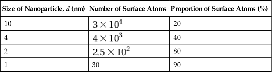
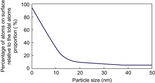
As can be seen from Figure 1.10, the percentage of surface atoms will rapidly increase because particle size is less than 10 nm. As the particle size reduces to 1 nm, the surface atomic percentage will be approximately 90%, and the atoms are almost concentrated on the surface of nanoparticles. As the particle size becomes smaller, the number of atoms at the surface will comprise a larger proportion compared with the number of internal atoms. An increase in the number of surface atoms, the smaller atomic coordination, and the high surface energy combine to present high surface activity. Meanwhile, these atoms will become extremely unstable and easily combine with other atoms. For example, nanoparticles of metal can burn in the air. In addition, they will adsorb gases and react with them. Another example is copper. For copper particles of 100 nm in diameter, the surface area ratio is 6.6 m2/g, and 10-nm particles have a surface area ratio of 66 m2/g. When the particle size is as small as 1 nm, the surface area ratio will increase to 660 m2/g.
Activity of surface atoms can induce atomic transport and surface nanostructure changes, and also can lead to conformational changes of spin and electron spectroscopy. An extreme case is the carbon nanotube, which contains only surface atoms, without any internal ones.
1.3.6 Dielectric Confinement Effect
Materials essentially have dielectric properties in addition to the dielectric loss, which constitute the most important physical characteristics of dielectric materials. Polarization of conventional materials is associated with the orderly structure; however, in the structure there is a significant difference between nanomaterials and conventional coarse-grained materials. Nanomaterials have their own unique dielectric behavior (dielectric constant, dielectric loss) that is mainly found in the dielectric constant and dielectric loss, which are strongly dependent on particle size. Frequency of the electric field may have a strong effect on dielectric behavior.
When nanoparticles are dispersed in heterogeneous dielectric materials, the interface can produce dielectric enhancement of the system. This phenomenon is called the dielectric confinement effect [9]. It mainly comes from the surface of particles and the local area inside.
When there is a significant difference in the refractive index between medium and particles, a border of the refractive index will appear. This leads to a marked increase of field strength at the particle surface and inside, rather than of the incident field strength. This enhancement of the local area is known as dielectric confinement.
Dielectric confinement effects of nanoparticles are important for light absorption and photochemical and nonlinear optical properties. The effect on the absorption of light reflected in the absorption spectrum is shown with a clear red shift. It is easy to understand this phenomenon. Because of the fact that the size of nanoparticles is smaller than the free range of the carrier, the photovoltaic composite carrier can be lowered. As the particle size decreases, the nature of particles will be strongly influenced by the surface state. When materials with a smaller dielectric constant are modified at the surface of the semiconductor ultrafine particles, larger changes take place in their optical properties compared to those of bare ultrafine particles. This is because, in relation to the surrounding medium of the exposed particles, the power line of the charge carrier surrounded in ultrafine particles can easily pass through this layer of film. Therefore, the shielding effect is weakened while the Coulomb force between charged particles is enhanced, resulting in enhancement of excitons in binding energy and oscillator strength. In the absorption spectrum, this is reflected by a clear red shift.
In the Brus formula, we can give a quantitative or qualitative analysis [10] of dielectric confinement effects of optical absorption band edge shift (blue shift, red shift). The Brus formula indicates that:
Here, ![]() is the nanoparticle band gap in absorption,
is the nanoparticle band gap in absorption, ![]() is the bulk band gap, r is the particle radius, and
is the bulk band gap, r is the particle radius, and ![]() is the equivalent quality of the particle, where
is the equivalent quality of the particle, where ![]() and
and ![]() are the effective mass of the electron and the hole respectively. The second item is the quantum confinement item (blue shift). The fourth item is the effective Rydberg energy. The third item is dielectric confinement, and it is defined as negative. Therefore, it causes a red shift of the absorption spectrum.
are the effective mass of the electron and the hole respectively. The second item is the quantum confinement item (blue shift). The fourth item is the effective Rydberg energy. The third item is dielectric confinement, and it is defined as negative. Therefore, it causes a red shift of the absorption spectrum.
Transition metal oxides, such as Fe2O3, Co2O3, Cr2O3, and Mn2O3, and other nanoparticles, while dispersed in sodium dodecylbenzenesulfonate, will present enhanced third-order nonlinear optical effects. Measurements of Fe2O3 nanoparticles found that the third-order nonlinear coefficient ![]() can be as high as
can be as high as ![]() , which is higher by two orders of magnitude in the water. This third-order nonlinear enhancement is also attributed to the phenomenon of the dielectric confinement effect.
, which is higher by two orders of magnitude in the water. This third-order nonlinear enhancement is also attributed to the phenomenon of the dielectric confinement effect.