
Superconducting Nanomaterials
Superconductivity is an important physical property of materials that occur at the nanoscale. As one can imagine, the applications of achievable superconductivity are significant, potentially changing the electronics world we know today. In this chapter, the physical principles of superconductivity are discussed, and how researchers are now using principles of nanotechnology to increase the superconductivity temperature of many materials.
Keywords
Superconductivity; BCS theory; Cooper electron pairs; quantum computers
8.1 Superconductivity [1]
Superconductivity is defined as electrical flow through a material with zero electrical resistance. In metals it occurs at very low temperatures, but higher temperature superconductivity occurs in some ceramic materials. Materials with superconductivity are called superconducting materials. In 1911, Heike Kamerlingh Onnes, a physicist at Leiden University, first discovered the phenomenon that at superconductivity of 4.2 K (i.e., −268.8°C, known as the transition temperature or critical temperature, Tc), the electrical resistance of mercury suddenly disappears. In 1933, Meissner found that when a substance in the superconducting state was applied with a magnetic field, magnetic field lines could not penetrate the sample while maintaining the magnetic flux inside the superconductor as zero. This feature is called the Meissner effect and is the second characteristic of superconducting materials. The third characteristic is the Josephson effect. Superconducting electrons may be in the formation of Cooper pairs. Cooper pairs can come through the barrier at a certain probability, known as the tunneling effect of Cooper pairs. In other words, the Josephson effect is a phenomenon whereby current comes through the two kinds of superconducting materials separated by a thin insulating layer in between. It was theoretically predicted by Josephson in 1962. Josephson was awarded the Nobel Prize for this work in 1973.
Superconducting materials have significant applications as low-loss current conductors, creating ultrahigh magnetic fields, and in microwave applications. Because of its enormous economic potential, it has been given increasing attention. There have been important research results and discoveries over the years, perhaps most noted by Nobel Prize awards to scientists in superconductivity research in 1913, 1972, 1973, 1987, and 2003.
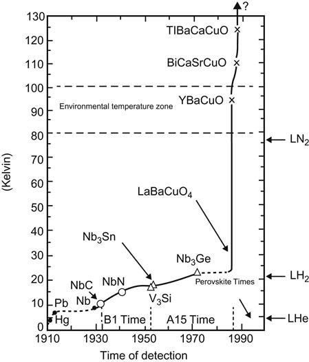
Considerable progress has been made in superconducting materials research. Nonetheless, the current Tc of superconducting materials remains very low. The highest transition temperature (Tc~130 K) is obtained by the use of copper oxide high-temperature superconducting materials. This temperature is higher than the boiling point of liquid nitrogen, so it can be used in many applications. At present, all the world’s applications of superconducting devices cannot operate without liquid nitrogen or liquid helium cooling equipment, which is expensive and inconvenient. It goes without saying that if superconductivity can be achieved at room temperature, then modern science and technology will certainly undergo profound changes (Figure 8.1).
Over the past 20 years, the exploration and discovery of new types of superconductors have changed our understanding of superconductivity. Researchers used to think that superconductivity was a rare phenomenon that would appear only at ultralow temperatures. Now, we have realized that superconductivity is a basic state of many materials, even those compounds that have little metallic character.
8.2 The Physical Principles of Superconductivity [1]
Ever since the phenomenon of superconductivity was discovered, researchers have been eager to reveal the mystery of its physical mechanism. After years of studies, Bardeen, Cooper, and Schrieffer believed that superconductivity originated in the electron and lattice interactions. This theory is known as the BCS theory. As shown in Figure 8.2, when an electron A comes through the crystal lattice, due to the mutual attraction of the charges with different signs, positive charges in the positive ion dot-matrix of a crystal lattice will be close to electron A, resulting in a partial density increase of the positive charges. This may lead to a local excess of positive charges. This disturbance of the partial positive charge may spread in the form of a crystalline lattice wave, which will, in turn, affect the second electron, namely electron A may further attract the other electron B in an indirect way. Of course, there is Coulomb repulsion between the electrons. However, as long as the interaction of the electron and lattice is strong enough, the indirect effect of attraction between the electrons is likely to exceed the Coulomb repulsion, so that the electron pairs may have a net amount of interattraction. The result is that a bound state can be formed between them. This bound state is an electronic pair formed by two pairs of electrons, called Cooper pairs. From the momentum space, the two electrons are set with a total momentum of K. Cooper’s work showed that when K=0, the binding energy reaches its maximum, and electron pairing has the lowest energy. From the momentum space, the two electrons in Cooper pairs may involve a quantum state with a momentum that is equal in size and opposite in direction, and also include those with an opposite spin. In this case, the Cooper pairs have an energy that is less than that of the two electrons in “their own action” and thus are more stable.
In the Cooper electron pairs, momentum (speed) of a single electron can be different. However, the total momentum of each Cooper pair is constant. Metallic resistance in the normal state is caused by the electrons under the scattering of crystal lattice waves. However, in the superconducting state, the electrons form Cooper pairs, conducting continuous scattering. During this process, the total momentum is conserved, and thus the current also remains unchanged. This is the reason why superconducting current is unfettered. Positive ions in the crystal lattice have thermal vibration that makes these “lone warriors” in difficulties, resulting in energy consumption during the electronic movement. This explains the resistance existing in normal metals.
8.3 The Classification of Superconductors [2]
8.3.1 Low-Temperature Superconductors
Superconductors with the critical temperature below the liquid helium temperature are known as low-temperature superconductors. After discovering properties of mercury, researchers discovered superconducting characteristics in tin, lead, and many other metallic elements and alloys, as well as compounds, but their critical temperatures have remained very low (below the temperature of liquid helium). Through years of efforts, researchers now have discovered most metallic elements exhibit superconductivity. By the introduction of special techniques (such as high-pressure technology, technology in precipitation into a thin film at low temperature, and very rapid cooling), those metals that were once believed to be unable to turn into superconductors have achieved the state of superconductivity under certain circumstances.
8.3.2 High-Temperature Superconductors
Low-temperature superconductors below the liquid helium temperature have limited industrial applications. For this reason, the practical application of superconductors had been stagnant for quite some time before the discovery of high-temperature superconductors (HTSs). Finally, in 1987, superconducting technology achieved a decisive breakthrough. Based on iridium, barium, and copper oxide, American scholars Mow-Kuen Wu and Paul Chu made HTSs (YIBa2Cu3O7) with Tc in the range of 90–100 K. These temperatures are above the boiling point of nitrogen (77 K). We call such materials HTSs. The discovery of cuprate HTSs has had a great impact on science and technology. This finding is a significant indicator of the development of superconducting materials over the past 10 years, not only because of their many applications already known but also because they revolutionized the basis of condensed matter physics. The reconstruction of a new theoretical framework still continues but is controversial. Many researchers believed that “understanding of the high-temperature superconducting mechanism” is an open issue that is considered to be the most critical issue in condensed matter physics. The discovery of cuprate HTSs illustrates some of the facts. Superconductivity is no longer regarded as a phenomenon that occurs at low temperatures only. Room-temperature superconductivity is now considered possible.
Almost all of the HTSs that have been discovered since 1987 are copper-containing ceramics. Although the critical temperature has been greatly improved, the HTSs have not yet attained the necessary stability. Also, the carrying capacity has also slightly decreased. All materials with the highest critical temperature are complexes with low-dimensional structure, and each of them contains light elements in the chemical formula. The high phonon density of states and high energy are very attractive. However, before a widely accepted theory of HTSs is established, the real key factor must be determined. The application of superconductors seems to have a long way to go.
8.3.3 Other Novel Superconductors
The newly discovered superconductors are found widely throughout the periodic table, from lighter elements boron and lithium to the transition metal uranium series, and many complexes of transfer salts. Here, C60 may have a greater potential for development because of its greater elasticity, making it easier to be molded than the oxide ceramic, which has a hard and crisp texture. Moreover, it has a larger critical current, critical magnetic field, and coherence length. These characteristics make C60 superconductors more likely to be put into practical use. C60 is hailed as a “star” of new materials in the twenty-first century, for it has demonstrated a wide range of novel features and application prospects in machinery, light, electricity, magnetism, and chemistry. Some researchers predicted that the giant C240 and C540, once synthesized successfully, are likely to become superconductors at room temperature.
Some superconductors have a higher Tc, for example the alkali metal “bucky ball” AxC60 has a critical temperature at 33 K, and RNi2B2C and YPd2B2C have a critical temperature of 23 K. Some superconductors are very unusual, such as the heavy fermion superconductors CeMIn5 (M=Co, Rh, Ir), CePt3Si, and PuCoGa5, which have a critical temperature of 18 K. Sr2RuO4 has its parameters in p-wave symmetry. Ruthenium copper oxide is not limited to HTSs in its antiferromagnetic order, even if they are only at a distance of a few angstroms. Magnesium diboride (MgB2) has dual-band superconductivity and a superconducting transition temperature of 39 K. Discovery of magnesium diboride provided new ways to study the new class of HTSs with simple compositions and structures. Magnesium diboride can be easily synthesized for processing and can be easily made into films or wires. It can be used in power transmission, supercomputer devices, as well as CT scan imaging instruments. Its discovery brought excitement to the world of condensed matter physics. Superconducting boron-doped diamond is an interesting research topic in the field of electronics. NaXCoO2·H2O is associated with another very interesting new material system. In the case of high pressure, researchers have also found that many elements may have a higher Tc. Some elements, under a pressure of 1 million pascals, may have a Tc of more than 10 K, such as Li and S (Tc=17 K), Ca (Tc=15 K), and B (Tc=11 K). The recently discovered CaC6 superconductor has Tc of 11.5 K, which is twice the value of the critical temperature of graphite electrode compounds.
8.4 Nanosuperconductors [3]
8.4.1 Research Progress
Researchers are interested in the superconductivity of nanometer-sized materials for the following reasons. First, nanomaterials can be used to make ultrasmall superconducting devices such as quantum bits (to be introduced later). Second, when some or all of the material sizes of a system are equal to or smaller than the feature sizes of length, such as the penetration depth, coherence length, grain size, and cell size, new quantum effects will be seen. Superconductivity may occur in the state of ultrathin film, wires, and quantum dots, which correspond to two-dimensional, one-dimensional, and zero-dimensional (2D, 1D, 0D) systems, including human-made structures such as knots, mesh, or multilayer heterostructures. Two-dimensional superconductors have an ultrathin film nanostructure. In the superconducting state, properties of the material largely depend on the spatial dimensions. Three-dimensional materials have the strongest superconductivity. In superconducting wire and superconducting thin films, thermal fluctuations and quantum fluctuations play an important role and are able to change the transport properties of electrons through the weak link. When the superconductors become small or thin, they often lose their superconducting properties. Superconducting properties have not been found to exist in ultrathin films, but the study results from one-dimensional superconducting coil are encouraging. As mentioned, in the superconductor, the current is hosted by the electrons in a configuration of Cooper pairs. Typically, the pairing of electrons has opposite spin and momentum; at any one time, an electron spins up and shifts to the left, then the other electron spins down and moves to the right. The force applied by the magnetic field will try to undermine the balance of the electron movement while keeping the spin directions of both of the two electrons arranged toward the magnetic field. Of course, due to the need for enough energy to undermine the Cooper pair, superconductors can withstand a certain intensity of magnetic field before being converted into the state of a normal conductor. This field is called the critical magnetic field. It may limit the application of superconducting coils and disable the superconducting coil to transfer high current, because the magnetic field generated by currents could weaken or destroy the coil superconductivity.
Phil Adams and his colleagues at Louisiana State University produced superconducting thin beryllium with a thickness of 2–30 nm in glass substrates [4], on which a 0.5-nm thin film of gold was precipitated. They found that when the magnetic field was applied in the direction parallel to the film, this gold–beryllium membrane could withstand a magnetic field much higher than that of pure beryllium film. In the thinnest films of 2 nm, the critical magnetic field was increased 10-fold. Adams and his collaborators believed that, in their case, the most critical factor was the interaction between the electron spin and the large positive charge in gold nuclei. Because of the relative movement between the electrons and nuclei, the action of a charge on another charge is equivalent to the occurrence of current, and the current would produce a magnetic field. The magnetic field produced by gold nuclei is much larger than that generated by the beryllium nuclei, so this magnetic field that comes from gold nuclei would cause each pair of Cooper electrons to be arranged in slightly the opposite direction. These distorted electrons are more easily adaptable to an external magnetic field because their spin in the rearranged direction is closer to the direction of the magnetic field. However, if the magnetic field is not parallel to the film, then the magnetic field would destroy superconductivity by interfering with the balance of the electronic movement rather than the spin. Although practical applications are still some way off, Adams saw the potential in the form of multilayer (sandwich) structures in the design of ultra-wires. These ultra-wire coils are likely to produce a stronger magnetic field than the presently used magnet, which is normally used in nuclear magnetic resonance instruments and physics research fields. Singular effects, demonstrated by Adams and his colleagues, provided the potential to help researchers in their study of Cooper pairs in HTSs, whose superconductivity is still not fully understood.
We know that superconductivity comes from “Cooper pairs” formed by spin-pairing electrons. When a superconductor is placed in a strong magnetic field, the electronic Cooper pairs will be destroyed. Meanwhile, the spin of electrons will also be affected, and the superconductivity will be weakened or completely disappear. But when the size of superconductors is reduced, the destructive effects of the magnetic field will also be weaker; when the superconductors become the size of the nanometer scale, the magnetic field will be unable to undermine the Cooper pairs. Bezlia Kim, a professor of physics at the University of Illinois, and associates confirmed this in their experiments. They placed a single layer of carbon nanotubes on the silicon wafer and these were etched with a “ditch” approximately 100 nm wide; the surface of carbon nanotubes was coated with a layer of Mo–Ge superconducting material. The temperature decreased below the critical temperature and the response of the nanoscale superconducting material in a strong magnetic field was observed. It was found that the impact of the strong magnetic field was significantly weakened on the nanoscale superconducting materials. Bezlia Kim and associates hypothesized that because of the very small ultra-wire diameter, only approximately 10 nm, interaction between the electronic Cooper pairs offsets the effects of the magnetic field on superconductivity.
This feature of nanoscale materials will broaden the application prospects for superconductivity. For example, in the past, superconducting coils could not transport high current because the magnetic field generated by currents could weaken or destroy the superconductivity of the coil. However, if the general nanoscale superconducting coil is mixed with the superconducting filaments, then transmission of strong current can be easily accomplished. In addition, the nanoscale superconducting material can also be used for magnetic resonance imaging and in other applications.
Certainly, the size of nanoscale superconducting materials cannot be infinitely reduced; if that were possible, then the mutual interference between the electronic Cooper pairs would undermine the superconductivity. In addition, the nanoscale superconducting materials cannot reach zero resistance consistently. This is similar to large superconducting materials.
In the past 20 years, researchers have made considerable progress in the preparation and characterization of nanostructured superconductors, including nanoparticles, quantum dots, nanowires, ultrathin film, and single-layer superlattice materials. In the field of high-temperature superconducting materials, many have lengths of only nanometers (e.g., single-crystal domain size, coherence length, etc.). Therefore, the experimental study of the nanometer-sized structures has considerable significance in helping researchers understand the mechanisms of the microworld.
Many experiments have been performed with regard to the zero-dimensional tunnel junction, such as the experiments with the so-called completely confined system. The capacity in preparation of low capacitance and small tunnel junction promoted research on the transition between the similar Josephson and charge performances in various Josephson junctions and junction arrays. The latter is the phase model of a physical instance of the shift from superconductivity to insulator, whereas the former shows the dissipation that reduced quantum fluctuations, thereby changing superconducting behavior. Therefore, through dissipation that reduces the quantum fluctuations, we can control the transition from superconducting to insulating. Technology in ultrasmall tunnel junction structures is essential to the study of the quantum bit (qubit). The qubit is one of the basic elements for building a quantum computer. Studies of the double tunneling junction have revealed the characteristics of the Coulomb blockade and odd–even effect that may be found in superconductivity.
Some features of one-dimensional nanowires have already been mentioned in the preceding chapters. The development of e-beam lithography makes it possible to perform structural design at an order of magnitude close to the superconducting coherence length. This has stimulated enthusiasm in physics research of superconducting nanowires, which are prepared by using growth approaches such as lithography and electrochemical templates with carbon nanotubes as template. A recent study reported the inverse proximity effect in superconducting wire: when the electrodes in contact with superconducting wire also show superconductivity, the superconductivity of the wire is then curbed. Perhaps this is an example of dissipation control of superconductivity. Another study showed that after the chaotic nature of the superconducting wire reaches a certain level, superconductivity completely disappears (the wire shifts from superconductor to insulator). This quantum shift is observed in the nanowire template constructed. The critical point can occur in the form of the critical resistance or the critical diameter, where the critical resistance is close to the quantum resistance (h/4e2), whereas the experiment showed a critical diameter of approximately 6 nm.
The emergence of two-dimensional ultrathin superconducting films provided a research platform for the topological phase transitions. The Kosterlitz–Thouless–Berezinskii transition [5] is a typical case of contemporary condensed matter physics.
For disordered films, a further decrease of thickness leads to the superconductor–insulator transition (rather than the superconducting metal transition). This transition can be adjusted by changing the degree of disorder, magnetic field, or electrostatic charge. This phenomenon, as an example of a quantum phase transition, recently created great interest. However, the basic principle of this phenomenon is unclear.
Heterostructures and superlattices are layered structures that contain an interface between different materials. Their nature is strikingly different from that of those composing materials. Sandwich junctions have been used to study superconductivity and other competing order parameters with respect to the interactions between them. Particular attention has been given to the interface between superconductor (S) and ferromagnetic (F) or antiferromagnetic (AF) materials. In an FSF three-tier structure, the transport process that came through the iron magnetosphere led to the emergence of a π-junction. Many superlattice materials composed of nano-size thin layers have been synthesized and studied. Recently, research attention has shifted to SFSFS-type superlattice material. Superconducting thin films have been found to have considerable unconventional quantum phenomena, such as the oscillation of critical temperatures and critical current density acting as a function of the thickness of magnetic iron, which were predicted earlier and have now been observed.
8.4.2 The Main Difficulties
For copper salts with high critical temperature and Sr2RuO4 or heavy fermion superconductors, the fundamental knowledge needed to discover this type of unconventional novel superconductor in low-dimensional geometry is currently lacking.
8.4.2.1 Incredible Magnetic Nanoclusters
Recent theory proposed that globular clusters with a specific number of superconducting electrons will show superconductivity at relatively high temperatures. This theory may be established for some simple metal clusters such as aluminum, gallium, zinc, and cadmium. For example, Ga56 was predicted with a critical temperature of approximately 150 K (−123°C). Mesh material composed of such clusters can be formed on the surface and can carry the superconductor current at higher temperatures. In 1984, W. Knight discovered the existence of the so-called shell structure, which is the basis of this phenomenon. At that time, this event did not arouse the attention of the superconductivity research community. Rather, it was largely ignored because of research on the cuprate HTS discovered in 1986, a hot topic at the time. At present, research on nanoclusters is steadily developing. It is quite possible that superconductivity will be observed in these clusters. Experiments in this area require artificially measuring the selected cluster concerning its excitation spectrum at low temperatures (above the critical temperature). Superconducting pairing mechanisms will lead to significant differences in the excitation spectrum at temperatures such as the critical temperature. Relevant technologies have been developed in this respect, including mass spectrometry, generation of an energy beam at different temperatures, as well as photoelectron spectroscopy. Another noteworthy achievement is the growth of isolated clusters in the matrix and molecular crystals, which can form an orderly three-dimensional lattice.
8.4.2.2 Quantum Fluctuations and Strong Correlation in Nanowires
Researchers have not yet come to any conclusion regarding the exact role that quantum fluctuations play in superconducting nanowires. The issue has aroused the interest of the scientific community in low-temperature superconducting electronics technology, because it may limit the length of the nanowire dimensions.
With the one-dimensional limit, the traditional Fermi liquid theory is no longer applicable; it is replaced by the Tomonaga–Luttinger liquid theory [6]. In the latter theory, there is no quasiparticle, and the excitation system is based on completely decoupled and separately excitable spin and charge degrees of freedom. This has been observed in filaments based on GaAs heterostructures. The relationship between the superconductivity and Luttinger liquid and the possibility of the Luttinger liquid itself being a superconductor is an interesting open issue.
8.4.2.3 Ultrathin Film
The open issues in this area include the following: the existence of an intermediate metallic regime in two-dimensional systems with Cooper pairs like ultrathin films rather than the nonelectronic type of quasi-particles such as the charge carrier; whether the insulating state is a new state of matter of the Bose insulator; and whether there are similarities between ultrathin films of superconducting behavior and the pseudo-gap regime of underdoped cuprate superconductor.
8.4.2.4 Proximity Effect
In the synthesis of nanomaterials, boundaries, crystal defects, chemical defects, and inhomogeneous strain may frequently cause the system to have various forms of “disorder,” thus affecting the properties of the materials. Physicists knew that when the superconducting material got close to nonsuperconducting materials such as excess oxides, pollution, impurities, and the substrates, a “proximity effect” might occur. This is because the Cooper pairs could get inside the normal material to a certain extent, whereas the normal atoms would have an impact on the superconductors. As a material gets smaller in physical size, its electronic wave functions, electromagnetic fields, and other properties will also make a difference. Therefore, in addition to the inherent nature of the material, we need to understand its nature in proximity to other materials, as well as the features it exhibits when reduced to nanoscale. As a result of the superconducting proximity effect, when a normal metal (N) touches superconducting materials, superconductivity will penetrate into the normal metal. The production of the proximity effect can be attributed to the coherence in electron transport passing through the metal/superconductor interface, a process called Andreev reflection. Regarding the proximity effect, we know it is a local effect. In copper salts, however, we have observed a long-range proximity effect, and there has been no explanation for this.
8.4.2.5 Nanosuperconductors and Hybrid Structures
In this regard, research directions include the fluctuation in nanosuperconductors, Josephson array, shot noise and dynamics, Andreev state and related phenomena, small Josephson circuit and the vortex dynamics in the Josephson array, nonstationary effect in meso-scale superconductors, and ferromagnetic/superconducting heterogeneous structures. By using the method of atomic layer molecular beam epitaxy (MBE), multilayer types have been greatly expanded. This method can also be used in the design of novel functional heterogeneous structures, including spin effects. This heterogeneous structure would also provide the conditions for basic research into the interaction between the magnetic order and the superconducting regions.
8.4.2.6 Links Between Superconductors and Nanostructure
The proximity effect and nanotechnology together can upgrade the traditional transmission and magnetic properties of superconductors. This effect had been predicted and then observed a long time ago, but it was only in recent years that, because of continuous improvement of the advanced technology in preparation of nanostructured materials, its different parameters and scope of applicability were substantially broadened. For example, in the interaction between the nanostructured magnetic particle arrays and superconducting thin films, simultaneous interaction with the vortex lattice may lead to a pinning effect. Arrays of magnetic particles can be prepared with the help of a variety of electron beam lithography or self-assembly, combined with sputtering or MBE and other thin film deposition technologies. Due to the geometry of the pinning arrays, resistivity of magnetic particle arrays, their magnetization, and other physical properties will show cyclical changes. Asymmetric magnetic nanostructures will produce a ratchet effect. The interactions between vortex and nanostructured arrays are considered in a certain frequency range to enhance a similar Josephson effect so the frequency range can be adjusted by an external magnetic field.
Based on the proximity effects of the two materials, boundary conditions and geometry of the nanointerface connecting with the superconductors will lead to the emergence of a novel electronic structure. For example, the common electronic reflection on the superconducting interface may become one that contains Andrew reflections, resulting in novel standing-wave states in small samples.
8.5 Application of Nanosuperconductors
Nanometer-sized materials can be used to make ultrasmall superconducting devices, such as quantum computing devices. Currently, use of the nanosuperconducting Josephson junction as a qubit is an ideal candidate among a number of quantum bits.
8.5.1 Quantum Computers
The quantum computer is a class of physical devices that can perform high-speed mathematical and logical operations and that can store and process quantum information following the laws of quantum mechanics. When a device’s processing and calculation are based on quantum information and run with quantum algorithms, it is a quantum computer. The concept of the quantum computer stems from research on reversible computers. The purpose is to address the issues regarding energy consumption of computers.
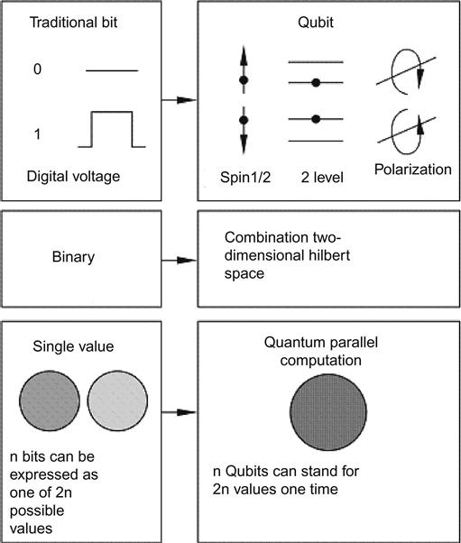
In the 1960s and 1970s, researchers discovered that energy consumption would lead to overheating of computer chips, which greatly affected the integration scale, thus limiting the ultimate speed of computers. Studies found that energy consumption comes from the irreversible operations in calculations. So, must calculation involve irreversible operations to complete? The answer is, for all the classic computers there is the possibility of a corresponding reversible computer with unchanged computing power. Because every step of the operation can be converted into a reversible operation, in quantum mechanics it can be expressed as a unitary transformation. The early quantum computer was a classical computer described by quantum mechanics languages and did not involve the use of the essential features of quantum mechanics, such as quantum superposition and coherence. In a classical computer, the basic information unit is a bit; the computing object is various bit sequences. Similarly, in a quantum computer, the basic information unit is the quantum bit, with operation targeting qubit sequences. The difference is that the quantum bit sequences not only are located at all orthogonal superposition states but also can be at the entangled state. In addition to the possibility of quantum parallel computing, these particular quantum states also brought about many wonderful features. In contrast to classical computers, quantum computers can perform arbitrary unitary transformation. Obtaining the output state, measurement can lead to the computing results. Thus, quantum computing generated a tremendous expansion of classical calculations. In the form of mathematics, classical computing can be seen as a special class of quantum computation. Quantum computers may transform a stack of each component; all of these transformations are completed at the same time and would stack at a certain rate of probability to give the results. This calculation is called quantum parallel computation. In addition to parallel computing, quantum computers have another important use, that is, to simulate quantum systems. This is a task beyond the competency of classical computers (Figure 8.3).
Whether using quantum parallel computing or quantum simulation computing, both are required to make use of quantum coherence. Unfortunately, it is difficult to maintain quantum coherence in a practical system. In quantum computers, quantum bits are not an isolated system. Rather, they will interact with the external environment, leading to the attenuation of quantum coherence, namely decoherence. So, the core issue in designing a quantum computer is to overcome decoherence. The discovery of quantum coding is by far the most effective way to overcome decoherence. The major quantum coding schemes include quantum error-correcting code, quantum error-avoiding code, and quantum error-prevention code. Quantum error-correcting code is the classic analog error-correcting code, which is a class of codes that attracted the most attention from researchers. Its merit lies in its wide application, but its drawback is its lower efficiency.
So far, there are still no quantum computers in the real sense in the world. However, many laboratories around the world are pursuing this goal with great enthusiasm. Many methods have been proposed regarding how to realize quantum computing. The problem lies in the fact that achieving the experimental manipulation of the micro-quantum state is very difficult. The currently available programs are mainly based on the interaction of atoms and cavity, as well as cold trap bound ions, electron or nuclear spin resonance, quantum dot manipulation, and superconducting quantum interference. It is difficult to say which option is more promising. From the perspective of integration and miniaturization, the quantum point program and superconducting Josephson junction program combined may be most appropriate. In the future, perhaps a novel design will emerge and make all the existing proposals obsolete; the new method might be based on some kind of novel material. Quantum computers are not intended to replace existing classical computers. The concept of quantum computers provides a new perspective for computation and is different from other new concepts of computers, such as optical computers and biocomputers. The role of quantum computers is far more than to solve some intractable problems that are possibly found in classical computers.
8.5.2 Nanosuperconductor Quantum Bits [7–10]
The production and control of the stable qubits system is a key issue in the practical use of current quantum information and the physical implementation of quantum computing. For nonsolid qubit systems, researchers have successfully demonstrated the operation of quantum logic gates and simple quantum algorithms. Nevertheless, practical quantum computing needs to overcome many known and unknown difficulties and to transcend some barriers of principles and nonprinciples.
To achieve practical use of the quantum computer in physics, we need to organically integrate universal quantum logic gates, to keep quantum entanglement between qubits, and to be able to manipulate them. With the increase in the number N of integration of qubits, the loss of quantum coherence (or quantum decoherence) will increase exponentially at the power of e. Recent studies have shown that the loss of quantum coherence of a single particle may decay at the index of e. But with the use of quantum entanglement with the characterization of complicated entanglement (concurrence), it will be almost lost in a limited period of time. These results suggest that a multi-qubit being simply integrated would have more vulnerable quantum coherence. Basically, this is a challenge to current theoretical and experimental subjects.
Microscopic quantum systems, such as atoms, spin, and photons, are easy to separate from the environment, thereby reducing decoherence, which is the advantage of the microscopic quantum system. However, the microscopic quantum system does not facilitate the integration to create the actual quantum computing devices. From this point of consideration, the macrosystem appears to be more flexible in the use of standard integrated circuit technologies. Macroscopic quantum bits currently proposed are based on nanostructured electronic circuits, or on the composition from the quantum dots, or by the superconducting Josephson junction. Josephson junction quantum bits are divided into three categories: charge qubits, flux qubits, and the corresponding hybrid qubits.
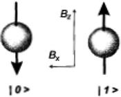
In fact, any physical system can be used as qubits, as long as it can be clearly defined with the two-level state. For example, the spin 1/2 particle in a magnetic field, with the spin only taken as +1/2 or −1/2 along the magnetic field direction, can constitute a two-level system (Figure 8.4).
A long time ago, researchers discovered that superconductors could exhibit the phenomenon of macroscopic quantum transport. Because of the superconductor coherence of Cooper electron pairs, all the microelectron pairs can be regarded as a single macrowave function. The tunneling nature shown by the macroscopic quantum wave function can be observed in the superconducting Josephson junction system. At present, the superconducting Josephson effect can be used to produce quantum devices that have advantages such as easy operation, longer coherence time, and ability to integrate for production as one of the potential quantum bit systems. Some superconducting quantum devices have been developed in the past, including quantum interference devices (SQUID) (flux qubit) and the single-electron device (charge qubit); all have been confirmed preliminarily to be excellent quantum bits. Here, we introduce their principles and characteristics.
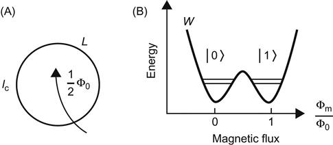
The flux qubit is as shown in Figure 8.5A. The SQUID quantum interference device is a superconducting ring, on which there are one or several Josephson junctions. The SQUID level constitutes a two-level system (Figure 8.5B). Here, the role of the Josephson junction covers two aspects: one is to separate the superconducting phases on the right and left sides and the second is to allow superconducting Cooper pairs to come through in the form of electron tunneling. Superconducting current coming through the Josephson junction is determined by the superconducting phase difference between the left and right sides ![]() . When the phase difference is zero or an integer multiple of 2π, the current is zero and the system has the lowest energy. Generally, the Josephson junction energy is expressed as
. When the phase difference is zero or an integer multiple of 2π, the current is zero and the system has the lowest energy. Generally, the Josephson junction energy is expressed as ![]() . Interestingly, as an external magnetic field is applied perpendicular to it, the magnetic field will cause an increase of one phase in superconducting quantum wave functions along the direction of the ring. Mathematically, this increased phase is expressed as the line integral of vector spaces, equivalent to the magnetic flux coming through the superconducting rings. Due to the single-valued nature of the superconducting wave function, the phase added to an external magnetic field must be compensated by the phase difference between both sides of the Josephson junction. If the phase difference is not zero, and if the superconducting ring is to produce a superconducting current around it, similar to shielding current, also known as persistent current, then, in fact, this persistent current can produce a magnetic flux
. Interestingly, as an external magnetic field is applied perpendicular to it, the magnetic field will cause an increase of one phase in superconducting quantum wave functions along the direction of the ring. Mathematically, this increased phase is expressed as the line integral of vector spaces, equivalent to the magnetic flux coming through the superconducting rings. Due to the single-valued nature of the superconducting wave function, the phase added to an external magnetic field must be compensated by the phase difference between both sides of the Josephson junction. If the phase difference is not zero, and if the superconducting ring is to produce a superconducting current around it, similar to shielding current, also known as persistent current, then, in fact, this persistent current can produce a magnetic flux ![]() . Here, L is the self-inductance of superconducting rings. The Josephson junction has a superconducting phase difference that satisfies the equation:
. Here, L is the self-inductance of superconducting rings. The Josephson junction has a superconducting phase difference that satisfies the equation:
(8.1)
 , and the horizontal level is representative of a mixed-energy state.
Here, ![]() is the magnetic flux contained in the ring, including the applied external field
is the magnetic flux contained in the ring, including the applied external field ![]() and the combined effect of continuous current.
and the combined effect of continuous current. ![]() is a constant and
is a constant and ![]() is magnetic flux in the magnetic field that causes an increase in phase of
is magnetic flux in the magnetic field that causes an increase in phase of ![]() .
.
Another type of superconducting quantum bits are charge qubits. We can use the phase conjugate physical quantities, that is, electric charge, as the two basic states of quantum bits. The principle of charge qubits is similar to that of single-electron devices. Figure 8.6A shows a typical superconducting single-electron device.
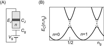
In addition, the smaller Josephson junction area of connected devices plus the lower volume of the central superconducting region (also known as the island, or box) may then reduce the equivalent capacitance of the central island. This creates Cooper pairs with a charging energy E for access to the central island greater than the disturbance of heat energy. Therefore, at low temperatures, we can see that the Cooper pairs are hindered in their access, with the whole line rendering a breaking circuit phenomenon, which is called the charge effect. Interestingly, when we use the gate voltage to change the potential energy of the central island, the electron energy for the access of a Cooper pair can be changed to zero. At this point, the line turns into an access but the charge transfer can only come through a central island one-by-one. When the charge effect arises, the amount of charge on the island becomes an important physical quantity. In general, we can write the following Hamiltonian to describe it:
(8.2)
Here, n represents the charge amount on the island described in the number of Cooper electron pairs. ![]() is the superconducting phase of the central island. ng is the equivalent amount of charge caused by the gate voltage. Because
is the superconducting phase of the central island. ng is the equivalent amount of charge caused by the gate voltage. Because ![]() and n are conjugates, and because the contribution that can be obtained from Josephson energy is actually +1 or −1 in the number of Cooper electron pairs on the island:
and n are conjugates, and because the contribution that can be obtained from Josephson energy is actually +1 or −1 in the number of Cooper electron pairs on the island:
(8.3)
As ng changes between 0 and 1, the lowest two energy states are n=0 and n=1. If we consider only two states, n=0 and n=1, then it can be viewed as a two-level state. Described in a spin 1/2 model, 4EC(1−2ng) is the magnetic field in the z direction, whereas EJ is that in the x direction. An ideal superconducting charge qubit can be the connection between the left and right sides to form a Josephson junction with two superconducting rings, similar to a quantum interference device, and may be called the controlled SQUID. The benefit is that as we change the magnetic flux coming through the superconducting rings, the equivalent of the Josephson coupling can be adjusted as ![]() , the principle described previously. Therefore, we can regulate the size and direction of the equivalent magnetic field by changing the gate voltage and magnetic flux. Devices of this kind are not in a simple two-level state. To simplify the infinite charge states into two, we must widen the energy gap for each energy state. To achieve this, we require EC
, the principle described previously. Therefore, we can regulate the size and direction of the equivalent magnetic field by changing the gate voltage and magnetic flux. Devices of this kind are not in a simple two-level state. To simplify the infinite charge states into two, we must widen the energy gap for each energy state. To achieve this, we require EC![]() EJ.
EJ.
In fact, more and more types of superconducting devices can be used as quantum bits. A suitable two-level state that can be found is not necessarily required to be the magnetic flux or charge. For example, a single Josephson junction can be used as qubits. In the Josephson junction system, there is a natural formation of energy levels with equal intervals of ![]() . A current coming through the Josephson junction tilts the wave-like potential energy wells equivalent to the Josephson effect. Under certain conditions, two more stable phase states can be acquired while the other higher energy states would decay quickly. The remaining two stable states become quantum bit systems that we need. Further manipulation of the quantum bits can be performed by changing the current size and the Josephson coupling energy. But its impact is less straightforward, as for the magnetic flux and charge qubits described previously.
. A current coming through the Josephson junction tilts the wave-like potential energy wells equivalent to the Josephson effect. Under certain conditions, two more stable phase states can be acquired while the other higher energy states would decay quickly. The remaining two stable states become quantum bit systems that we need. Further manipulation of the quantum bits can be performed by changing the current size and the Josephson coupling energy. But its impact is less straightforward, as for the magnetic flux and charge qubits described previously.
Another possible improvement is the use of a Josephson ![]() junction to supersede the current 0 junction. General Josephson junction has a current of zero if the phase difference is zero. The
junction to supersede the current 0 junction. General Josephson junction has a current of zero if the phase difference is zero. The ![]() junction has a current of zero if the phase difference is
junction has a current of zero if the phase difference is ![]() . This is equivalent to the potential energy curves of the 0 junction being translated for a distance of
. This is equivalent to the potential energy curves of the 0 junction being translated for a distance of ![]() . This makes the superconducting rings using a
. This makes the superconducting rings using a ![]() junction in the absence of the applied field able to automatically achieve the two magnetic flux states from energy degeneracy. At present, there are three types of experimentally feasible
junction in the absence of the applied field able to automatically achieve the two magnetic flux states from energy degeneracy. At present, there are three types of experimentally feasible ![]() junctions. The first is the use of d-wave properties of HTSs, in which the superconductor crystal plane is rotated by 90° to complete the bonding. The second includes a magnetic metal layer being added to the middle of the superconductor junction. Magnetic material flipping its electron spin is used to change the phase of Cooper electron pairs in tunneling. The third involves a metal layer being added to the middle of the superconductor junction, which is injected with high-energy electrons. Inside the metal layers, the electronic distribution of a nonthermal equilibrium state may result in changes in the relationship between superconducting current and phase. Because the third type of junction is located in a high-energy excited state, one can imagine that its systems may have a very short coherence time. For this reason, research on quantum bits is more prone to obstacles. They can be fine-tuned from the 0 junction to the
junctions. The first is the use of d-wave properties of HTSs, in which the superconductor crystal plane is rotated by 90° to complete the bonding. The second includes a magnetic metal layer being added to the middle of the superconductor junction. Magnetic material flipping its electron spin is used to change the phase of Cooper electron pairs in tunneling. The third involves a metal layer being added to the middle of the superconductor junction, which is injected with high-energy electrons. Inside the metal layers, the electronic distribution of a nonthermal equilibrium state may result in changes in the relationship between superconducting current and phase. Because the third type of junction is located in a high-energy excited state, one can imagine that its systems may have a very short coherence time. For this reason, research on quantum bits is more prone to obstacles. They can be fine-tuned from the 0 junction to the ![]() junction for a single device. Theoretically, another particular Josephson junction was proposed, which is formed by the combination s-wave–d-wave–s-wave, with the received energy of the Josephson junction being −EJ cos(2γ). Linked with the general Josephson junction in the parallel state, it can also be a quantum bit device.
junction for a single device. Theoretically, another particular Josephson junction was proposed, which is formed by the combination s-wave–d-wave–s-wave, with the received energy of the Josephson junction being −EJ cos(2γ). Linked with the general Josephson junction in the parallel state, it can also be a quantum bit device.