
Semiconductor Quantum Dots
One of the more exciting classes of nanomaterials is semiconductor quantum dots. Due to quantum confinement effects associated with their nanoscale size and structure, amazing optical properties are obtainable for materials absorbing and emitting light from the UV to the NIR. In Chapter 4, quantum dots are discussed. A physical basis of the quantum confinement effect is described, which is then used to explain the unique optical properties these materials exhibit. Applications of quantum dots are also described in detail.
Keywords
Quantum dots; quantum confinement; quantum excition; quantum dot emission; quantum dot lasers
In the middle of the past century, the advent of silicon-based semiconductors and transistors combined with the successful development of silicon-based integrated circuits triggered the electronics industry revolution. In the early 1970s, quartz fiber-optic materials and GaAs lasers were invented to promote the rapid development of fiber-optic communications technology, effectively catalyzing the start of the information age. In 1970, L. Esaki and R. Tsu (both working for IBM) proposed the concept of superlattices [1] and contributed to the quick development of low-dimensional semiconductor materials. This completely changed the design concepts of optoelectronic devices, such that the thought process for design and manufacture of semiconductor devices went from “impurity management” to the area of “band engineering.” The development and application of nanoscience and technology will enable the capability to control, manipulate, and manufacture powerful novel devices and circuits at the atom, molecule, and/or nanoscale, potentially changing our current standards of life as we know it.
Beginning in the 1970s, research on low-dimensional semiconductor quantum structures has had a rich 30-year history. Currently, the electronic or optoelectronic devices in a III–V quantum well structure have been commercialized. These materials helped achieve high-speed electronic devices and high-performance luminescence detectors. Quantum dots (QDs) are a class of zero-dimensional material, sometimes referred to as artificial atoms. Research on QDs has led to applications in light-emitting devices and detectors.
In addition to its application in electronic or optoelectronic devices, QDs can be used to manufacture qubits. For example, the charge of a QD can be used in the definition of quantum bits: one extra electron stands for “1” and none stands for “0.” Some have suggested that the electron spin states (spin up or spin down) can be considered as “0” and “1.” Recent research is more focused on the use of the exciton state in QDs; when the QDs absorbed the energy that is precisely from the photon excitation, a self-excited electron will enter the conduction band while leaving a hole in the valence band. Electrons and holes are paired to reduce energy by Coulomb attraction, resulting in the formation of excitons. Excitons have fairly long lifetimes, with relatively sharp radiation lines, and are easy to excite and detect with optical characterization methods.
There is a great deal of optimism surrounding the potential of QDs in quantum computing. However, despite all the excitement surrounding QD-based computing along with the various theoretical work put forward by researchers, no one has been able to test the quantum-bit logic operations. Experimental techniques are still lacking regarding the control and measurement of the QD process.
4.1 The Physical Basis of Semiconductor QDs [2]
4.1.1 Quantum Confinement Effect
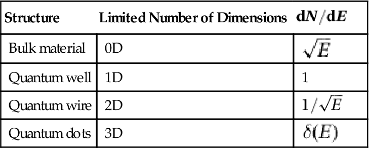
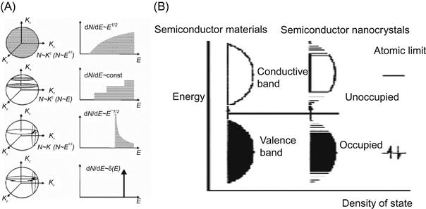
Because electrons are limited in movement along certain directions, the electron energy in that direction would have been quantized. This is because in this direction, the bound electrons would lead to the formation of standing waves. According to the number of binding dimensions, we can classify materials into bulk material (0 binding dimension, 0D), quantum well (one binding dimension, 1D), quantum wire (two binding dimensions, 2D), and QD (3 binding dimensions, 3D). Energy quantization may have a great impact on materials in terms of the electronic density of states (DoS), which is defined as
DoS=dNdE=dNdkdkdE
For example, for the 3D case, N(k)=k![]() space volume/volume of each state, then
space volume/volume of each state, then
N(k)=4/3πk3(2π)3/V
The carrier density difference in the structure with different dimensions is as shown in Table 4.1 and Figure 4.1.
Table 4.1
Expressions of Carrier DoS in the Structure with Different Dimensions
| Structure | Limited Number of Dimensions | dN/dE |
| Bulk material | 0D | √E |
| Quantum well | 1D | 1 |
| Quantum wire | 2D | 1/√E |
| Quantum dots | 3D | δ(E) |
Discrete states are caused by quantum confinement and are obtained with the energy-level solution of the Schrödinger equation:
−ℏ22m∇2Ψ+V(r)Ψ=EΨ
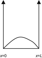
For example, in the case of the one-dimensional infinite square potential well, its solution is
Ψ(x)~sin(nπxL)
where n is an integer. Here, the ground-state wave function is as shown in Figure 4.2. If the restrictions apply only in one direction (e.g., x), then the other two directions of energy are still continuous. The total energy is
n2h28mL2+p2y2m+p2z2m
For the 3D infinitely deep square potential well (quantum box),
Ψ(x,y,z)~sin(nπxLx)sin(mπyLy)sin(qπzLz)
Here, n, m, and q are integers. Energy level is
En,m,q=n2h28mLx2+m2h28mLy2+q2h28mLz2
This is the simplest case. Rather than an infinite depth of the box, the actual potential barrier can also be spherical, restricted, or exhibit harmonic oscillator potential limitations. Note that we considered only one electron in this case. In the actual situation, it is often required to deal with multiple particles and electron–hole pairs. Particle mass also requires consideration, along with potential mismatch at boundaries of particles.
The size of QDs is in the range of approximately 10–100 nm, which is equivalent to the de Broglie wavelength of electrons in semiconductors. Thus, the electron or hole would be subject to three-dimensional quantum confinement effects and have quantized energy levels, forming the so-called zero-dimensional electronic system. As mentioned, QDs are often referred to as artificial atoms. The main reason is that QDs have an electronic configuration that is very similar to that of atoms, so energy levels of QDs are often introduced with symbols such as s, p, and d, which are referred to as the ground states of QDs and the excited-state levels.
Take the InAs QDs, for example. Their geometric shape is similar to a flat convex lens; therefore, the potential energy in the r direction can be approximated with a two-dimensional paraboloid. This approximation tells us that the ground state and the excited state have a number of degeneracy, respectively, 2, 4, 6, and so on (including spin degeneracy). In other words, QDs can be filled with two electrons, p energy levels can be filled with four electrons, and so on. Clearly, the QDs are not the same in electronic configurations with the atoms. In the orbit as s, p, d, the atomic energy levels can be filled with the numbers 2, 6, 10, and so on. This difference is mainly rooted in the QDs with essentially different forms of potential energy from the atoms. The atomic potential energy is mainly formed in the Coulomb interaction, with three-dimensional symmetry. However, the potential energy form of QDs is directly related to the geometric shape. Because its shape is similar to a convex lens, its height is much smaller than the diameter. Therefore, electrons in QDs have only two-dimensional (plane) symmetry, with the degeneracy form of energy levels unlike that of atoms.
4.1.2 Excitons and Luminescence [3]
4.1.2.1 The Concept of Excitons
Due to Coulomb forces, excited electrons and holes can be tied together to form bound electron–hole pairs, for example the excitons. In a semiconductor, the electron and hole are of attracting potential, where the hole has an effective mass greater than the electron effective mass, leading to the formation of a hydrogen-like atomic system. Exciton binding energy is determined by the Bohr theory:
En=−e22εa0n2;a0=εh24π2μe2here,μisthereducedmass.
In the QDs, excitons may arise from within the QDs and are subject to them, with the restriction extent decided by their size. An exciton also has discrete energy levels, so an absorption peak similar to the δ![]() function is presented in the exciton absorption spectrum.
function is presented in the exciton absorption spectrum.
4.1.2.2 Energy Band Structure of Excitons
At zero temperature, the semiconductor band is structured with a filled valence band and an empty conduction band. Between the top of the valence band and the bottom of the conduction band, there is a gap with no electrons, called the band gap. In terms of the symmetry of the cubic lattice, the top of the valence band is the state equivalent to angular momentum l=1![]() . Due to the interaction of spin and orbital, a fourfold degeneracy of state is formed as
. Due to the interaction of spin and orbital, a fourfold degeneracy of state is formed as
(j=l⊕s=3/2,mj=±1/2,±3/2)
commonly known as heavy hole,
|32,±32⟩
and light hole,
|32,±12⟩
The light and heavy holes are classified according to the size of the effective mass in the vertical interface. Taking into account the role of limitations in the vertical direction, usually the side width of QDs is much larger than that in the vertical direction, exhibiting strong limitations in the vertical direction. The light-hole band is held down because of a small effective mass. So, the absorption of light close to the energy gap comes from a major contribution of the heavy holes.
An electron, when excited from the valence band into the conduction band, will leave a similar positively charged hole. Driven by Coulomb attraction between the hole and electronics, the electrons are combined into an exciton state. Binding energy released in the formation of the exciton is only 6 meV in bulk materials. Regarding two-dimensional quantum wells, the effects of the limitations can increase the binding energy of the exciton by 15 meV (simply interpreted as the positive and negative electron distance being compressed, thus resulting in the increase of the Coulomb force). In the QD structure, exciton binding energy will be further released by approximately 20 meV. Exciton band energy is equal to semiconductor band gap Eg![]() , coupled with the binding energy of electron and hole from limited effects Ee
, coupled with the binding energy of electron and hole from limited effects Ee![]() , Eh
, Eh![]() and minus the binding energy to form excitons Eb
and minus the binding energy to form excitons Eb![]() :
:
Eex=Eg+Ee+Eh−Eb (4.1)
Specifically, Figure 4.3 shows exciton e 1s and h 1s
E1s1sex=Eg+E1se+E1sh−E1s1sb
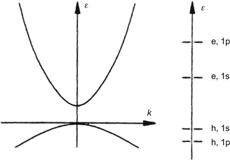
Figure 4.4 shows exciton e 1p and h 1p
E1p1pex=Eg+E1pe+E1ph−E1p1pb
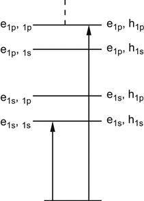
When the electron and hole in the excitons recombine, a photon is emitted that is equal to the energy difference between valence and conduction states. The exciton lifetime can be as long as a nanosecond (10−9 s) and, as such, is readily observable with various experimental techniques, allowing the possibility to study the quantum evolution of the excitons.
When the excitation light to generate the electron–hole increases, we need to consider the multi-exciton states. Because there are a number of electrons and holes, two separate excitons may be close to each other to form coupled pairs of exciton states, which have energy of 1 meV, which is lower than that of the independent pairs of exciton states. Now laser can have a frequency stabilized to 4 neV (4×10⁻⁹ eV). Thus, it is not difficult to distinguish between these two states in experiments. Figure 4.5 shows an energy band diagram of multiple excitons in typical GaAs QDs: g is all electronic valence bands in the vacuum state and ε+![]() is an exciton state excited by the D-light:
is an exciton state excited by the D-light:
hole|32,−32⟩andelectron|12,−12⟩
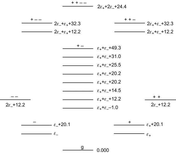
ε−![]() is an exciton state excited by the L-light:
is an exciton state excited by the L-light:
hole|32,+32⟩andelectron|12,+12⟩
Here, ε++ε−−1.0![]() for the combination state of a D-exciton and an L-exciton, with energy less by 1.0 meV compared with that of the two separate excitons.
for the combination state of a D-exciton and an L-exciton, with energy less by 1.0 meV compared with that of the two separate excitons.
4.1.3 Calculations of the Exciton Binding Energy [5]
For spherical QDs, without considering the case of Coulomb interaction, the Schrödinger equation of an electron or hole can be written as
−ℏ22mi∇2ςi(r)=εiςi(r) (4.2)
Here, i![]() is electron or hole. Under the ideal quantum constraints, the boundary condition is
is electron or hole. Under the ideal quantum constraints, the boundary condition is
ςi(r)=0forr=R (4.3)
With the boundary conditions for Eq. (4.3), the Schrödinger equation (4.2) is solved as
ςi(r)=√14πR3jl(αnlr/R)jl+1(αnl)Yml(θ,ϕ) (4.4)
Here, jl![]() is l-order spherical Bessel function. αnl
is l-order spherical Bessel function. αnl![]() is the n th root of l-order spherical Bessel function. With the spherical Bessel function, boundary conditions for Eq. (4.3) can be written as
is the n th root of l-order spherical Bessel function. With the spherical Bessel function, boundary conditions for Eq. (4.3) can be written as
jl(αnlrR)|r=R=0 (4.5)
that is
jl(αnl)=0 (4.6)
We substitute Eq. (4.4) into Eq. (4.2) to get a discrete eigenvalue
εi=ℏ22mi(αnlR)2 (4.7)
Using the band zero point at the valence band maximum, with Eq. (4.7) type, the energy levels of electrons and holes are
εe=Eg+ℏ22me(αneleR)2 (4.8)
εh=−ℏ22mh(αnhlhR)2 (4.9)
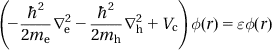
As mentioned, the single-particle spectrum is not in line with the optical absorption spectrum, because it does not take into account the Coulomb interaction between electrons and holes. The Schrödinger equation to describe electron–hole pairs is
(−ℏ22me∇2e−ℏ22mh∇2h+Vc)ϕ(r)=εϕ(r) (4.10)
 (4.10)
Applied here are the usual spherical coordinates with the boundary conditions ϕ(r=R)=0![]() , and Vc
, and Vc![]() is Coulomb potential. If the impact of Coulomb potential is not included, then Eq. (4.10) can be resolved to get the energy of electron–hole pairs using
is Coulomb potential. If the impact of Coulomb potential is not included, then Eq. (4.10) can be resolved to get the energy of electron–hole pairs using
ε=εe+εh=Eg+ℏ22me(αneleR)2+ℏ22mh(αnhlhR)2 (4.11)
and the wave function
ϕ(re,rh)=ς(re)ς(rh) (4.12)
where
ς(r)=√14πR3jl(αnlr/R)jl+1(αnl)Yml(θ,ϕ) (4.13)
When considering the Coulomb potential, Eq. (4.10) cannot yield an exact numerical solution. The variation method is commonly used [6].
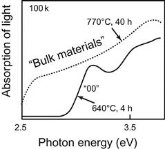
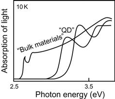
Figures 4.6 and 4.7 show the linear absorption spectra of CdS crystals and QD in glass at room temperature and 10 K. Clearly, for QD, the spectrum line is more acute and easy to distinguish.
4.2 Preparation of Semiconductor QDs [7,8]
Semiconductor QDs have a heterogeneous structure in the nanoscale, which is coated by a lower energy gap of the semiconductor nanostructures in another material with higher energy gap. At present, methods for QD synthesis are mainly divided into the following.
1. Chemical colloidal method: By way of chemical synthesis of sol, this method can be used to produce multilayered QDs. This is a simple process that can be used in mass production.
2. Self-assembly method: Molecular beam epitaxy (MBE) or a chemical vapor deposition process is used. The principle of lattice mismatch is used so that the growth of QDs can undergo self-polymerization in a particular substrate. This method is applicable for mass production of QDs that are regularly arranged.
3. Lithography and etching: A beam or electron beam is applied directly on the substrate, which can be etched to produce the pattern. This process is time consuming and not applicable for mass production.
4. Split-gate approach: An external voltage is applied to generate a two-dimensional confinement to the two-dimensional plane of the quantum well. The gate is controllable regarding changing the shape and size of QDs and is suitable for academic research rather than for mass production.
Preparation of QD technology is established on the basis of a thin film growth process. Current literature often cites three kinds of classic models for thin film growth:
1. Layered growth (Frank–van der Merwe (F-M)) mode
The F-M model is based on single start, and then there is growth of a second layer; that is, layer-by-layer growth. The growth of crystalline thin films is basically decided by the crystalline direction of the first layer. In the case of heteroepitaxy, more or less lattice mismatch may exist between the growth film and substrate, resulting in thin film stress.
2. Island growth (Volmer–Weber (V-W)) mode
In V-W mode, the atoms are first deposited on the exposed surface of the substrate and will gradually form a small island, which may also increase at the same time, or decompose into single atoms. Meanwhile, prior to the formation of thin film, rearrangement over a wide range is possible, causing the so-called coarsening. The crystalline direction of the growth film cannot be quickly determined in the growth process.
3. Mixed growth (Stranski–Krastanov (S-K)) mode
The S-K model is a mixture of layered growth and island growth. This model generally starts from layered growth. After that, island growth takes over on one or a number of growth layers.
Because self-organized growth can produce QDs with superior optical properties and is compatible with conventional device technology, it has been highlighted in recent years. Self-organized growth can be obtained via MBE or the metal organic chemical vapor deposition (MOCVD) method. Three-dimensional island substances can be naturally formed between the two kinds of materials with mismatched lattices in a specific growth pattern.
The following is an example of the sample growth method for indium arsenide QDs. It illustrates the preparation technology of semiconductor QDs.
By use of the MBE technology and S-K growth mode, the growth of indium arsenide QDs is as follows. Normally, the n-doped 100 surface of GaAs is used as substrate. Hydrogen-ion plasma is first used to remove the surface oxide at approximately 610°C, and then growth of a buffer layer with thickness of approximately several hundred nanometers occurs. The temperature is adjusted down to 500°C (usually between 450°C and 550°C) for the growth of the epitaxial layer of indium arsenide, and its thickness increases along with the generation rate and time. Before obtaining 1.8 monolayers (ML), obvious QDs will not appear. However, when the thickness exceeds 1.8 ML, that is, when it exceeds the threshold thickness, an indium arsenide layer will form the pattern of self-assembled QDs (SAQDs). The quality of QDs, such as the dot size, density, uniformity, morphology (shape), and so on, is greatly relevant to the growth methods, conditions, and parameter settings. High-quality growth technology of QDs can be state of the art. The QD covered with a layer of gallium arsenide may lead to the formation of a QD device with a sandwich structure. This part is the active layer in laser diodes. Also, to effectively confine the carriers in small spaces (carriers confinement) and for optical confinement where resonant cavities can be generated to induce luminescence, both sides of the active layer can, respectively, experience growth of a barrier layer of the part with the different n (or p) concentration of arsenic aluminum gallium alloy composition, enabling the generation of effective carriers that can reach the active layer to allow the occurrence of compound-emitting radiation. The outermost p+ (or n+) highly doped layer is mainly for the formation of ohmic contacts with electrodes.
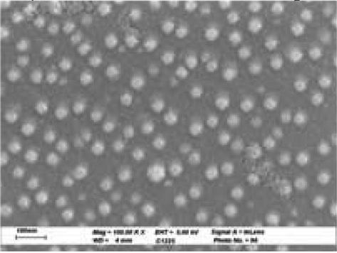
After the growth of a QD sample, a field-emission scanning electron microscope (FE-SEM) can be used to observe their geometric morphology and measure the surface density (QD/cm2) of QDs. The growth quality of QDs is essential for the performance of QD lasers and is quite sensitive to the growth methods and conditions. Take gas-phase MBE growth as an example. The crystalline dimension of the gallium arsenide substrate (100 or 111), doped composition, growth temperature, the vapor pressure of arsenic, element ratio of III/V, growth rate, the interruption mode and time, composition and thickness of overgrowth layer or cap layer, and the growth pattern of the sub-monolayer of indium and gallium may affect the quality of the growth of QDs. Figure 4.8 shows a two-dimensional image captured by FE-SEM on InAs/GaAs QDs.
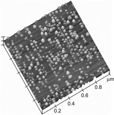
Apart from using FE-SEM to measure the density of QDs, high-resolution transmission electron microscopy can accurately measure the size of the QD (height×base area). Atomic force microscopy (AFM), scanning tunneling microscopy, or scanning probe microscopy can also be used for observing geometry and measuring QDs. Figure 4.9 shows a two-dimensional image obtained by atomic force microscopy on InAs/GaAs QDs. QD density is generally between 1×10⁹![]() and 1×10¹¹
and 1×10¹¹![]() cm−2. The bottom diameter is approximately tens of nanometers, and the height is approximately a few nanometers. The QD size, density, and the growth conditions and the parameter correlation are described in detail here. If you are interested in this subject, please refer to the recent literature of nanotechnology.
cm−2. The bottom diameter is approximately tens of nanometers, and the height is approximately a few nanometers. The QD size, density, and the growth conditions and the parameter correlation are described in detail here. If you are interested in this subject, please refer to the recent literature of nanotechnology.
4.3 Laser Devices Based on QDs [7]
Semiconductor QDs have many important applications. Here, we use an example to introduce the current status of their application in the field of laser devices.
Since the inception of quantum well structures [1], researchers around the world have carried out much theoretical work, expecting to apply quantum mechanism in semiconductor laser technology, and then their interests shifted to quantum wires and QDs of lower dimensions. In 1982, Arakawa and Sakaki at the University of Tokyo performed theoretical calculations and indicated that QDs have three-dimensional electronic limitations and the energy DoS in the form of a δ function. Meanwhile, they theoretically predicted the performance qualities of the QD laser, which include low threshold current, high temperature characteristics, and high glow efficiency. Compared with conventional semiconductor lasers, QD lasers show great improvements in thermal stability. In 1986, Asada predicted through calculation of theoretical means that the threshold current density with the QD structure will be significantly lower compared with that with a one-dimensional quantum well structure, which indicates a new direction for solving the problem of having a threshold current density that is too high, which is a problem encountered with semiconductor lasers. At that time, however, the production of QDs was based on lithographic technology, which made it difficult to get high-quality, nanoscale QDs. Although the quantum size effect with experimental results has confirmed the theoretical predictions one-by-one, the production of high-performance QD lasers has always failed.
In the mid 1980s, with the development of semiconductor epitaxy techniques (e.g., MOCVD and MBE), it was possible to control the growth of semiconductor thin film materials precisely and to access high-quality two-dimensional restricted quantum well and superlattice materials. Made from these two-dimensional materials with confinement heterostructure, the performance of optoelectronic devices, such as lasers and detectors, has seen rapid improvement. Their products quickly entered the market and acquired a wide use. Tremendous success in two-dimensional quantum well materials encouraged researchers to continue to try to restrict electron movement in more dimensions and launched experimental studies of quantum wires and QDs.
In 1994, the research team of Marzin used stress (geometric deformation) resulting from the lattice mismatch between the arsenide and indium gallium arsenide heterostructure layers to form SAQDs [9]. In the same year, N. Kirstaedter and N. N. Ledentsov reported the world’s first self-organized QD lasers on edge emission [10]. They inserted a gradient refractive rate into self-organized QDs with single-layer index InGaAS/GaAs, which were used for a separate confinement of heterostructure and the quantum well laser structure. The original quantum well served as an active medium, thus achieving a low current density threshold (120 A/cm2) at low temperature (77 K). After that, SAQDs have been receiving great attention. Extensive studies have covered topics from the basic physical properties of quantum devices to fabrication studies that helped obtain rewarding results. From 1994 onward, the field of QD lasers underwent rapid development. Low threshold current density, excellent thermal stability, and a variety of other fascinating properties have attracted much attention in a growing number of laboratories.
The years 1996 and 1997 witnessed a rapid development of QD lasers. A large number of international research teams have joined the ranks to fuel intense research into QD lasers. To achieve the ground state of QD lasers, optimizing conditions for the growth process have to be provided as the foundation for significant improvement in QD size and shape uniformity.
With in-depth studies performed in recent years, the actual produced QD lasers could have a current density threshold much lower than those of conventional and quantum well lasers. In 1996, N. N. Ledentsov used 10 layers of In0.5Ga0.5As/A10.15Ga0.85As in a QD superlattice structure as the active region for QD lasers so that at room temperature, the threshold current density decreased to 90 A/cm2. In 1999, G. T. Liu and colleagues successfully developed the InAS/In0.15Ga0.85As QD laser with threshold current density of 26 A/cm2 at room temperature. So far, QD lasers with HR coating on their sides have obtained a threshold current density of 10–20 A/cm2, which is two to four times lower than that of the best quantum well lasers. Of the lasers with multilayer QDs as the active region, QDs on each layer may have a low threshold current density, even as low as 7–10 A/cm2.
The temperature stability of QD lasers has also been increasing. In 1994, Kirstaedter reported the first electric-pumped QD lasers, which showed good temperature stability at low temperatures (150–180 K). At room temperature, however, the thermal stability of current density threshold was inferior to that of commercial GaAs quantum well devices. In 1997, Maximov and associates placed QDs into the GaAs/AlGaAs quantum wells. This approach led to an increase in the barrier height of escape of carriers in QDs, greatly reducing the escape probability of the carrier. Meanwhile, leakage current was reduced to yield a laser characteristic temperature T0 of up to 385 K at an operating temperature between 80 K and 330 K, well above the characteristic temperature of the quantum well laser. Nonetheless, an increase in T0 has led to a significant increase of the current density threshold. In 1999, Shernyakov reported the world’s first GaAs-based QD laser with operating wavelength of 1.3 μm, which is the first such device that works at room temperature but at the same time has both a high characteristic temperature T0 (160 K) and a low current density threshold Jth (65 A/cm2, three-layer QD arrays). Although the highest characteristic temperature T0 of InP-based quantum well lasers that work in the same band is 60–70 K, the lowest current density Jth threshold is 300–400 A/cm2.
For ideal QD lasers, QDs should have the same size and shape; that is, the QDs should be of one single electron and hole energy level, and should be easy to achieve in a single-mode operation. In 1996, Kirstaedter and associates at the temperature of 77 K with the density value slightly higher than the current density threshold (<1.1×Jth) observed single-mode operation. By contrast, quantum well lasers to achieve single-mode operations are required to be well above the threshold current density.
In 2004, the University of Tokyo and Fujitsu succeeded in the trial development of QD lasers that worked in the 1.3-μm wavelength; the optical power fluctuation caused by the temperature can be adjusted to approximately one-sixth the original value. Within the range of 20–70°C, it can send out optical signals steadily at 10 Gbit/s without the compensation of temperature-caused optical power changes. Eliminating the need for external circuitry for temperature compensation helps reduce the size of the optical transmitter and the overall cost of the product. The research team is currently trying to extend the free-to-adjust operating temperature range of the laser to 0–85°C. This significant progress contributes to the development of small optical signal transmitters with low cost and power consumption. The Metropolitan Area Network (MAN) and high-speed optical Local Area Network (LAN) are expected to benefit from it.
At present, QD laser materials have been discovered, but the best material thus far is still the arsenide indium (or gallium indium arsenide alloy) QDs with the growth of the III–V family on GaAs substrates. Indium arsenide has a narrow energy gap, which can be adjusted through the x value after adding a small amount of gallium component (InxGa1−xAs, 0![]() x
x![]() 1) for preparation of nanometer-sized QD structures. Furthermore, it can be used to produce laser light source or light-detecting devices with wavelengths in the range of 1.3–1.55 μm, which is suitable for use in optical communication. Here, we must point out that the laser light with wavelengths between 1.3 and 1.55 μm is vital because optical fiber has a very low energy loss in this band, quite suitable for long-distance optical communications.
1) for preparation of nanometer-sized QD structures. Furthermore, it can be used to produce laser light source or light-detecting devices with wavelengths in the range of 1.3–1.55 μm, which is suitable for use in optical communication. Here, we must point out that the laser light with wavelengths between 1.3 and 1.55 μm is vital because optical fiber has a very low energy loss in this band, quite suitable for long-distance optical communications.
QDs in the III–V family are valued mainly in the application of their optical and electronic properties, such as high-frequency (high-speed) electronic devices, high frequency light-emitting devices, and light detectors with high-efficiency. Measurement tools for study of QD optical properties include photoluminescence, time-resolved photoluminescence, and the temperature change experiments that come with the power changes in the optical excitation or pumping or the cryogenic systems, and these may obtain the radiation photon spectra of the e-hole recombination from spectral data and the relaxation mechanism and time of its carriers, life information, and other device-related parameters.
The development of QD lasers in recent years has made considerable progress and has launched a strong challenge to traditional semiconductor lasers, but there is still a large gap between its performance and theoretical prediction. The following problems must be addressed to further enhance the performance of QD lasers. First is the growth of size-uniform arrays of QDs. Although the QD material provides many potentially advantageous properties, its uneven size distribution makes the QD light-emitting peak have nonuniform broadening, whereas the luminescence peak is wide and much larger than that of the quantum well material (meV). In fact, only a small part of QDs contribute to the light-emitting process. This limits the optical gain and makes further reductions in the lasing threshold of the lasers difficult to achieve. Second is the ability to increase the surface density and volume density of QDs to maximize the material gain of QDs. Third is the ability to optimize the structural design of QD lasers so that it is conducive to QDs in the carrier capture and bondage. And last is the ability to control QD size or to select a novel material system for broadening the scope of work of the lasing wavelength of QD lasers to the band of 1.4–1.6 μm in Wavelength Division Multiplexing (WDM) networks.
For the indium arsenide QD materials, the current indium arsenide QDs have achieved considerable progress in laser diode devices. At a wavelength of 1.3 μm and a low critical current density (~19 A/cm2), it can launch a continuous single-mode wave in the operation mode at room temperature, with power of up to 210 mW. At present, the performance of QD lasers has been better than that of the InP quantum well laser, but its performance is not entirely satisfactory. To improve the effectiveness of indium arsenide QD lasers, we must also perform studies focused on reducing the critical current, improving the temperature characteristics in device operation (increase of the temperature of the device), and preventing the switch between the ground-state module and the excited-state module, as well as to improve laser luminous efficiency. Indium arsenide QDs still have a number of issues that need further study, such as high density, size, uniform epitaxial layer growth of QDs, as well as precise observation of QD shape and size measurements, the component analysis of inside and outside QDs and stress distribution of measurements or estimates, theoretical calculations of QDs with different morphologies on the quantum band and energy levels, energy value of electrons in the optical transition between energy levels, the relaxation mechanism of carrier energy, and the measurements of carrier lifetime and other main physical quantities. With the efforts of scientific researchers, more efficient high-power and single-mode high-quality laser devices in high-temperature operation with a wavelength of 1.3–1.55 μm will be developed.
4.4 Single-Photon Source
Quantum optics is focused on the study of the nature of light and the basic interactions between light and matter. Semiconductors are mainly related to the physical principles and applications of electronic materials and devices. Over the past few decades, quantum optics and semiconductors have been developing along separate paths. Specifically, quantum optics research is focused on the field of atomic and molecular optics. Over the past decade, rapid progress in semiconductors has been made in nano-related science and technology. People began to notice that some of the semiconductor mesoscopic systems and quantum systems can also be found with some quantum optical phenomena. In this way, a new area of research was discovered, known as “semiconductor quantum optics.” Even more specifically, there is a field in mesoscopic systems where quantum optical phenomena called “mesoscopic quantum optics” are discussed. In various types of semiconductor mesoscopic and quantum systems, the most notable is the QD system. QDs are called “artificial atoms” and have an energy level structure that is very similar to that of atoms. Therefore, it is not difficult to imagine that the quantum optical properties existing in a number of atomic and molecular systems can also be found in the semiconductor QD system.
Semiconductor light-emitting materials or devices (such as lasers and light-emitting diodes) serve as a medium to convert the carriers (electron and hole) into photons. If this conversion process is fast and efficient, then the statistical behavior of the carriers will be converted to that of photons. It is well known that electrons and holes are fermions, while photons are a kind of boson. Through proper device design, or in specific mesoscopic semiconductors and quantum systems, the photon statistics of radiation will be different from classical electromagnetic waves, and such light is also often referred to as “nonclassical light.”
Quantum optics has extremely important or potential applications in many areas, and the most notable area is quantum information, including quantum computing and quantum communication. In particular, the use of a single-photon source is expected to bring about the very promising quantum cryptography. Semiconductor quantum optics is particularly vital for the development of practical applications of quantum information. For example, by virtue of current technology, semiconductor quantum optics has been successfully applied in the production of highly efficient single-photon radiation, whereas the wavelength of operations can also be extended to that in the optical fiber communication band (1.3 μm). Applications of quantum cryptography in optical communication have already made significant progress.
The theoretical basis of quantum optics was first established by Roy J. Glauber in 1963; he also won the 2005 Nobel Prize in Physics for his outstanding contributions to quantum optics. The concept of optical quantization can be traced back to the blackbody radiation theory created by Max Planck in 1900 and the interpretation by Einstein of the photoelectric effects in 1905. However, the real birth of quantum optics theory is symbolized by an optical interferometer (often referred to as an HB-T interferometer), which was jointly designed by R. Hanbury-Brown and R. Q. Twiss between the years 1952 and 1956. This interference device was originally used to observe Sirius, and later it was used to observe the coherent characteristics of mercury, which then led to the surprising discovery of some positive coherence between the detected photons.
Figure 4.10A shows a schematic diagram of an HB-T interferometer device. A beam splitter divides the incident light into two beams. Meanwhile, two-photon detectors were used to observe the intensity coherence properties of incident light, which is usually expressed by second-order coherence function g(2)(τ). Here, τ indicates the time difference for two detectors in detecting photons, as shown in Figure 4.10B.
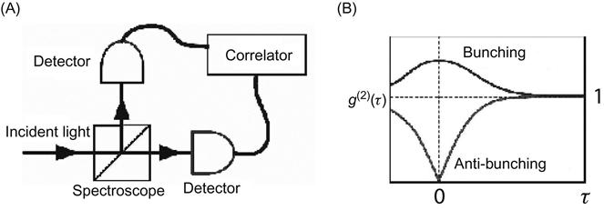
Coherent features can be distinguished by the use of the value g(2)(τ=0). If considering the incident light in particles, then g(2)(τ=0) can be regarded as the “possibility” of two detectors in simultaneously detecting photons. As g(2)(τ=0)>1, an increased likelihood that two detectors detect photons at the same time is observed. It can be said that incident light waves have positive coherence in time between them. E. M. Purcell thought at the time that such positive coherence could be explained using quantum statistics. Because photons are a kind of boson, when they have the same quantum state they tend to “gather” together to reach the two-photon detector at the same time. So, the phenomenon of light is also often referred to as the coherent cluster (bunching) effect of photons. In fact, the coherent features of light can also be interpreted using classical electromagnetic theory, so arguments between the two theories were ongoing at that time. In 1963, Glauber proposed the quantum theory of optical coherence, giving a reasonable explanation for the photon bunching effect observed in HB-T experiments. Now physicists know that the photon bunching effect is actually associated with characteristics of photons from thermal radiation, and coherent light (e.g., laser) does not have any positive correlation (i.e., g(2)(0)=1).
The quantum optics theory gives an interpretation of the photon bunching effect, and it also expected photons to show an anti-bunching effect in some cases. The anti-bunching phenomenon of photons was first observed by Kimble, Dagenais, and Mandel with the fluorescence of a single sodium atom in 1977. Because the classical electromagnetic wave theory failed to explain the “anti-bunching” phenomenon of light, the phenomenon used to be considered direct evidence of the quantum nature of electromagnetic waves. Light with anti-bunching characteristics has also been classified as “nonclassical light.” If a physical system has anti-bunching characteristics, then the system does not radiate two or more photons at the same time. In other words, the system only sends one photon at a time, so it is called a single-photon source.
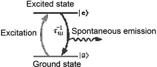
The anti-bunching phenomenon is a characteristic of fermions. A single-photon light source radiates photons with anti-bunching features, indicating that a single-photon light source has the characteristics of fermions. In fact, any single independent quantum system can produce single-photon radiation. As shown in Figure 4.11 with a two-level system as an example, the system includes a ground state and an excited state. The electron in the ground state, once excited by light or electricity, may jump to the excited state, and then back to the ground state through spontaneous emission. This process sounds simple but implies a mechanism of nonclassical light. As the electron falls in the scope of fermions, when it occupies the excited state but has not yet produced spontaneous radiation, we cannot excite the next electron to the same excited state. The time for an electron to occupy the excited state is related to the lifetime of spontaneous radiation. Therefore, in this period of time, even if constant excitation is given to this system, it will still not produce photons. Thus, an independent two-level system will be unable to simultaneously produce two or more photons and only constitutes a single-photon source.
As already known, there are many systems that can produce a single-photon source, including single-atom or single-molecule systems. Stability control of a single atom or molecule, however, requires complex technologies that may cause difficulties in practical applications. In addition to atomic and molecular systems, many of the solid-state systems also can produce single-photon radiation, such as the nitrogen vacancy center in diamond chemical combination and semiconductor QDs. They share a feature of the system with similar energy levels of atoms or molecules.