Chapter 7
Electronic Amplifiers in Microwave Photonic Links
7.1. Electronic amplifiers in optical links
The design of electronic amplifiers in microwave photonic links requires analog circuit design techniques for the lower part of the microwave spectrum but also microwave techniques above a few gigahertz. These steps give rise to numerous processes that are not discussed here. The appendix, section 7.4, outlines the different parameters used in circuit design and this Chapter discusses the paths and trends in the design of these circuits. It should be noted that numerous technologies are used for high-frequency circuits, e.g. Si CMOS technologies, bipolar Si/SiGe technologies or HFET, or HBT technologies on GaAs or on InP substrates. These technologies have been synthesized in [SCA 09], but the technologies are integrated in the form of monolithic microwave integrated circuit (MMIC) chips.
7.2. Amplifiers in the optical link emitter
7.2.1. Different roles of electronic amplifiers on optical emitter
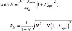
At a microwave photonic link input, there is an electronic amplifier performing several functions.
If the modulation signal is directly introduced on the laser biasing, the amplifier has a double function: it serves as an impedance matching between the 50 Ω of the microwave source and the few ohms of the laser input impedance and must also supply a non-negligible current to the laser input. For low frequencies, this matching is realized by a classical analog circuit and for frequencies greater than a few gigahertz, microwave amplifiers are needed.
If modulation is introduced via an external modulator whose input impedance is approaching 50 Ω, there is no need for impedance matching, but there must consequently be a voltage excursion (5 to 7 V peak to peak for impulse operation); high currents also have to be delivered as this excursion is over 50 Ω.
In both cases, the input amplifier can also work as a link noise mask, e.g. a 30 dB gain amplifier can restore the link noise factor from 30 dB to a few decibels. Obviously, a circuit design that does not introduce nonlinearity in the link is still required. The relations for nonlinearities given in Chapter 5 are of course valid for the electrical part of the circuits.
7.2.2. Emission: modulator or laser input amplifiers
7.2.2.1. Analog amplifiers
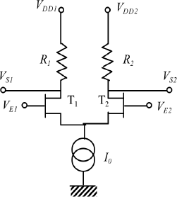
Link input analog amplifier circuits are generally designed to directly drive a laser or a Mach-Zehnder modulator. They must supply a biasing current to the laser or a biasing voltage to the modulator. A current must also be supplied as the modulator input impedance is around 50 Ω. It should be noted that such a circuit is more intended for digital modulation, but nothing prevents it from being used with an analog signal.
Figure 7.1 represents the different parts that constitute such a circuit, which has been realized with InP/InGaAs heterojunction bipolar transistor (HBT) technology [BAN 91]. The biasing and reference currents of the signal are applied to current mirrors. The signal is applied to a differential amplifier through a buffer amplifier, which is used for impedance matching to calibrate the signals applying to the differential pair.
As recalled in section 7.4, the circuits described can be found in studies about analog circuits, such as [GRA 09]. The circuit in the present example is only intended to drive a laser. Load RL represents this laser and a value of 3 Ω. Load RL is only present for symmetrical reasons. A modulation current IMD added to a biasing current IDC is applied to the laser. This type of circuit allows a modulation by signal imod, which can be digital, e.g. 10 Gb/s. This signal can also be an analog signal of a few gigahertz.
Figure 7.1. Laser amplifier circuit
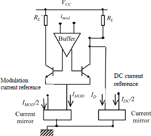
Figure 7.2. Complete circuit of a laser driver amplifier
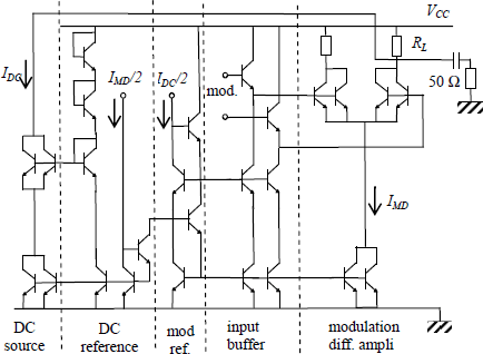
Figure 7.2 shows the complete topology of the driver circuit showing the connections between HBT transistors and the introduction of the circuit from Figure 7.1. The double transistors shown in the circuit have an emitter dimension (2.5 × 11 μm) allowing the generation of a 100 mA current. These have half the emitter length and appear as single transistors.
Other GaAlAs/GaAs [MON 91] or InGaP/GaAs [YAM 94] amplifier circuits based on transistors have been proposed in the same frequency range. The general circuit structure is the same and these circuits can drive lasers just as well as Mach Zehnder modulators.
7.2.2.2. Narrowband microwave amplifiers
In the case of a narrowband circuit, an amplifier is designed for a 50 Ω input and output matching impedances to drive the modulators and approximately for a 5 Ω output matching impedance to drive lasers. This amplifier type can be realized by focusing on the step proposed in section 7.4 or in [RUM 04c]. However, it must be noted that a laser can require a large current, implying power amplification design techniques.
7.2.2.3. Ultra wideband microwave amplifiers
In the case of a very wideband laser or modulator drivers, a distributed amplifier structure is needed (see section 7.4.8.3). This topology has been widely investigated and developed since the first circuit proposed in 1981 [AYA 81].
A first example provides an 8 dB gain amplifier between 1 and 18 GHz with a gate line (input) impedance of 50 Ω and a drain line (output) impedance of 10 Ω [DUE 97]. This amplifier has four AlGaAs/GaAs HFET transistors with 0.25 μm-length gates.
A second example [HAF 05] also requires a distributed amplifier but introduces several improvements on the design proposed in the first publication [RUM 04c]. The first improvement consists of using a cascode topology to improve isolation between the input and output. However, the cascode topology has a negative output resistance at high frequencies. Hence damping resistances must be added. Another aspect concerns a delivered output power above 20 dBm. For this, a large total transistor finger width is needed. Two different versions are proposed to deliver such a power.
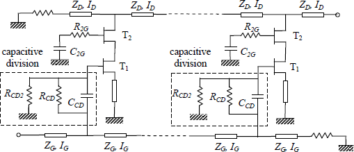
The first uses a six transistor-stage amplifier but each transistor presents a fairly strong input capacitance; this increasing losses in the distributed amplifier gate line which must have a characteristic impedance of 50 Ω. Each transistor input is thus preceded by a capacitive divider to diminish the apparent capacitance. This first amplifier has a 13 dB gain up to 40 GHz for the band to −3 dB. This amplifier drives a modulator with a power at 1 dB of compression of 24.6 dBm at 0.5 GHz and 21 dBm at 20 GHz. This corresponds to a peak to peak voltage of 7.2 V at 20 GHz. However, the weak gain forces the input amplifier to have two stages. Figure 7.3 illustrates this circuit which has six transistor-stages.
Figure 7.3. Capacitive divider distributed amplifier topology
A second configuration has nine cascode stages. This second version gives a gain of 20 dB up to 34.5 GHz for the bandwidth at -3 dB. This amplifier thus drives a single-drive modulator with a power at 1 dB of compression of 25 dBm at 0.5 GHz and 22 dBm at 20 GHz. This corresponds to a peak-to-peak voltage of 8.2 V at 20 GHz.
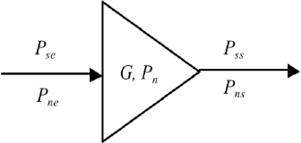
7.3. Receiver: amplifiers at the photodetector output
7.3.1. General points
The amplifier placed just after the photodetector must amplify the generally weak microwave signal. For a sufficient link dynamic range, this amplification must have low noise. Depending on the application, the photodetected microwave signal is narrowband or very wideband. Therefore several amplifier technologies can be used.
The equivalent electrical circuit to a photodiode is a low current source in parallel with a very high resistance Rd (e.g. 2 kΩ) and a capacitance Cd. The first amplifiers placed behind the photodiodes transformed a weak input current into a high output voltage. For these circuits a transimpedance (output voltage divided by input current) that is as high as possible is required and refinement consists of optimizing these transimpedance amplifiers (TIA). Elsewhere, this circuit should not increase the noise, thus low noise amplifiers are required. As the photodiode is equivalent to a capacitance, to have a high photodiode cutoff frequency, a very low receiver input impedance RC has to be used. As a result, the cutoff frequency is given by the expression:
![]()
For wideband circuits, this constraint dictates the input choices of the transimpedance amplifiers.
To have a very wide microwave frequency band (e.g. 40 GHz), the transimpedance amplifier was replaced or accomplished using an amplifier that was more appropriate for microwaves: the distributed amplifier.
When the microwave signal is of low bandwidth, it is possible to design a narrowband amplifier by compensating the photodiode capacitance using an inductive load. In this case, a compromise between the low noise and link output matching must be made.
If the photodetector is a phototransistor, the latter can be directly followed by an integrated amplifier designed in the same technology.
7.3.2. Transimpedance amplifiers
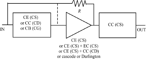
The topology of a transimpedance amplifier is given by Figure 7.12. Numerous transimpedance amplifier designs have been proposed using different technologies. Figure 7.12 was completed by an input stage and an output stage whereas the intended amplification stage was replaced by two cascade common emitter (source) stages or a common emitter (source) followed by a common collector (drain) stage or a Darlington stage or a cascode stage. The Darlington topology can only be designed using bipolar transistors. The resistive feedback is connected at the input or only on the central part. All these possibilities are represented in Figure 7.4 and each of them compensate for certain disadvantages.
The input stage was initially a common source stage then a common drain stage, but finally, it is the common gate stage which seems to best suit because of its low input impedance [VAN 93]. [SHI 01a] found a resistance of 31 Ω with this kind of topology.
Figure 7.4. Different variations of transimpedance amplifiers. CE, common emitter; CC, common collector; CB, common base; CS, common source; CD, common drain; CG, common gate
All types of transistors were used to design transimpedance amplification via one of the configurations illustrated in Figure 7.4. For a transimpedance amplifier with a bandwidth from 0 to fmax (fmax, frequency for which the transimpedance gain is equal to −3 dB) the relation between this frequency and the field effect transistor cutoff frequency or the transition frequency of bipolar transistors (in both cases called ft) is given by the expression below, which varies according to the references:
[7.1] ![]()
Transimpedance amplifiers were first realized with GaAs FETs [CAS 92], then AlGaAs/GaAs heterojunction bipolar transistors [GOV 93; NAG 94; PED 93; VAN 93], then InP/InGaAs bipolar transistors [GOV 93; SAM 96], then InAlAs/InGaAs HFET [AO 00] or InP/InGaAs HFET [SHI 01b; WU 03]. With their improved frequency performance, designs using SiGe/Si bipolar transistors [KIM 01] or CMOS transistors [HWA 06] were also proposed.
For example, Figure 7.5 illustrates a transimpedance amplifier design with an InP HFET [SHI 00; SHI 01b]. This amplifier presents an input impedance of 31 Ω, which contributes to a very wide bandwidth when coupled to a photodiode. It has a transimpedance gain of 8 dB up to 40 GHz. However, there is no indication of the level of noise produced.
Figure 7.5. Transimpedance amplifier circuit [SHI 00]
7.3.3. Distributed amplifiers
Regarding laser or modulator driver amplifiers, distributed amplifiers present another structure that enables very wideband amplifications for the receiver. They can be used as receivers as they have low noise values (3 to 6 dB).
These amplifiers have limited frequency via gate line and drain cutoff frequency and unlike transimpedance amplifiers (equation [7.1]), they more closely approach the maximum transistor frequency. Section 7.4 succinctly describes all the improvements to the basic structure (as presented in Figure 7.23) of distributed amplifiers.
One initial design proposed a GaAs FET base distributed amplifier [KIM 96b]. This amplifier benefitted from several improvements (listed in section 7.4.6.3). It has cascode topologies, loss compensations due to an inductance between the two cascode transistors, and an inductance in the gate of the second transistor. It also has an active load for the gate bias and a frequency-dependent collector line load. The two latter improvements allow a low frequency of 0 Hz for at least one stage.
This amplifier type was also realized using InAlAs/InGaAs/InP transistors with 0.1 μm-length gates [KIM 96a]. An initial amplifier design had eight 50 μm wide transistors (Figure 7.6), a 16 dB gain, a bandwidth of 47 GHz at 3 dB, and a noise value of 5 dB. A second amplifier design had six 25 μm wide transistors, a 10 dB gain, a bandwidth of 89 GHz at 3 dB, and a noise value of 6.5 dB. For amplifiers used in optical links, the group time must be constant as a function of frequency. This is the case for the second amplifier (constant group delay between 20 and 40 ps).
Figure 7.6. Distributed amplifier for eight 50 μm-length transistors [KIM 96a]
Distributed amplifiers have a relatively low gain, so several cascades are needed, in which case the link capacities limit low frequencies. Although quite complex, a solution was proposed, which consisted of introducing a voltage shift circuit (which was itself distributed) between the two distributed amplifier stages. This circuit is represented in Figure 7.7 and was successfully placed between two distributed stages composed of GaAs FET [KIM 95].
Figure 7.7. Eight transistor distributed voltage shift circuit [KIM 95]
7.3.4. Combination of transimpedance and distributed amplifiers
For an identical technology, transimpedance amplifiers will always remain at lower bandwidths than distributed amplifiers. However, their input impedance and noise figure can be lower. One solution is to cascade a transimpedance and distributed amplifier in which is anticipated a high frequency gain peak corresponding to the transimpedance amplifier gain fall.
This is proposed in [SHI 00; SHI 01b]. The cascade is achieved by direct coupling between an amplifier identical to Figures 7.5 and 7.6 composed of seven cascode mountings each with two InP HFET transistors with 0.15 μm gate length and 40 μm wide. It is thus possible to obtain a 52 dBΩ transimpedance on a band from 0 to 49 GHz. In this frequency range, the gain is 20 dB. This amplifier presents a 31 Ω input impedance and a group time of 55 ± 15 ps.
7.3.5. Narrowband amplifiers
In the case of a narrowband microwave signal, the receiver comes down to a much more classical low-noise narrowband amplifier design. It is schematized in section 7.4.
7.3.6. Preamplifier after a phototransistor
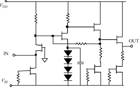
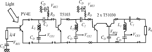
In this case, the principle consists of creating an amplifier using the same bipolar transistor technology as that used to create a phototransistor, as presented in [POL 04]. It uses InP/InGaAS heterojunction bipolar transistor technology with which the phototransistor presented in Figure 4.24 is created.
A narrowband amplifier is placed behind this phototransistor. The diagram of this amplifier is represented in Figure 7.8.
From the phototransistor described in Figures 4.24 and 4.25 (marked PV4 in Figure 7.8), this amplifier has a common emitter mounting followed by a cascode mounting created with an identical heterojunction bipolar transistor (T51030). These two mountings are input and output matched with classical localized microwave circuits. The optomicrowave gain of this amplifier is 7.5 dB at 31.7 GHz.
Figure 7.8. Narrowband phototransistor and amplifier [POL 04]
7.3.7. Other circuits after a phototransistor
To follow a phototransistor created using a transistor technology available in a foundry, it is possible to introduce other circuits than an amplifier.
Using InP/InGaAs HPT technology, a frequency converter oscillator is proposed in [GON 03].
Using Si/SiGe HPT technology, such as that presented at the end of section 4.3.4 (AMS technology), a microwave oscillator frequency modulated by a base band signal (FSK modulation) is proposed in [LEC 06].
7.4. Appendix: analog and microwave amplifiers
7.4.1. General points
This presentation is at the intersection of microwave and optoelectronic technologies. For those who practice the first domain, the design of electronic and microwave circuits is fairly conventional, but in the domain of optoelectronic it is not so obvious. Therefore this summary of the design of analog and microwave amplifiers is written for the designers of the second domain.
Electronically classic analog amplifiers (resistive amplifiers, resistive or transimpedance feedback amplifiers, differential amplifiers, Darlington mounting) always have a wideband. Numerous reports have presented designs of these amplifiers [GRA 09]. As for microwave amplifiers, they involve passive components, such as capacitances and inductances. They can be narrowband (frequency and bandwidth in the order of 10% when taking into account different attenuations), intermediate band (slightly lower than the octave), or very wideband. The detailed design steps can be found in [RUM 04c].
This section summarizes the procedures and constraints of analog and microwave amplifiers design [ALG 06]. The principle of microwave amplifier design is founded on S-parameters of the active component, such as bipolar or field-effect transistors. The most important consideration in amplifier design is stability, power gain, noise optimization, and the choice of biasing point.
7.4.2. Analog amplifiers
7.4.2.1. Transistor equivalent circuits
The equivalent circuit or diagram of a small or linear signal FET is given in Figure 7.9.
Figure 7.9. Small signal FET model
The equivalent circuit of a small signal bipolar transistor was given in section 4.4.
7.4.2.2. Common source mounting
This is the most used configuration for amplifier design to enable high voltage gain. The input admittance is dominated by capacitance Cgs. This capacitance influences the high cutoff frequency, hindering very wideband matching.
Capacitance Cgd is directly responsible for the input/output isolation degradation.
7.4.2.3. Common gate mounting
The input is applied on the source and the output signal is restored on the drain. The current gain is equal to 1: it is a current buffer stage. Its input admittance being large, the bandwidths are wider than those obtained with a common source mounting. Nevertheless, this mounting is the least used as the isolation between input and output is much lower, which leads to the risk of instability.
7.4.2.4. Common drain (or source follower) mounting
The input signal is applied on the gate and the output signal is taken from the source. The voltage gain is equal to 1, it is a voltage buffer stage. Input admittance is reduced to capacitance Cgd, which is lower than capacitance Cgs of a common source transistor. This mounting is often used as an impedance matching associated with voltage shifters (voltage shift diodes).
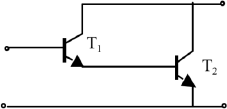
7.4.2.5. Cascode mounting
Cascode mounting is a combination of the two previous mountings, which the associated advantages and disadvantages of each: the bandwidth is wider and the isolation between the input and output is larger. This stage is illustrated in Figure 7.10.
Figure 7.10. Cascode stage
7.4.2.6. Darlington mounting
This mounting is only allowed with bipolar transistors and does not bias the second transistor base. As it has feedback, it allows a flat gain in a very wideband. It can be used in simple or distributed structures.
7.4.2.7. Very wideband and strong sensitivity amplifier: transimpedance amplifier
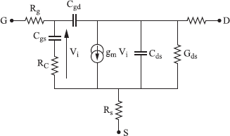
Optical fiber telecommunication systems require very sensitive receivers in order to maximize their transmission range. The transimpedance amplifier is a key element. It forms an interface between the weak current from the photodiode and the amplifier input, which precedes the decision circuit. This amplifier plays a pivotal role in the determination of receiver performance: the gains, sensitivity, and bandwidth of this circuit underlie the performance of the optical receiving chain. In general, a compromise must be made between the bandwidth and the sensitivity.
Figure 7.12. Transimpedance amplifier
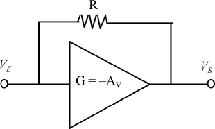
Transimpedance amplifiers use feedback, thus supplying a good compromise between noise and bandwidth. The disadvantage of this structure is that instabilities can arise.
The input impedance is low for a high gain and its dynamic range is important. The feedback resistance thermal noise appears as an additional noise source in parallel with the amplifier noise current. The noise is minimized by taking a large feedback resistance; however, in this case, the bandwidth is reduced.
7.4.2.8. Noise immunity: differential amplifier
The use of differential signals is very helpful in low signal applications. As a result, if the signal level is very low and/or the signal over noise ratio is low, the difference between two signals allows doubling of the signal level. Circuits using differential signals have better performance than single signal circuits in strong noise level environments. However, the gain-band product is more limited than for a distributed structure. The consumption and size are increased by the use of a transistor pair, which, generally, is associated with additional source follower stages.
The association of a transimpedance and differential amplifier allows gain increase by benefiting from the performance of an input transimpedance structure.
7.4.3. Microwave amplifier: expression of transistor reflection coefficients
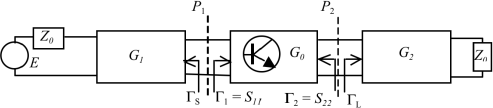
A bipolar or field-effect transistor is a three-port network as it has three access points: base-collector-emitter or gate-drain-source. Generally, the transistor is mounted as a common emitter, common source, or any other configurations. It is considered an active two-port network characterized by its distribution S matrix measured in comparison to the reference impedance Z0. The transistor is supplied at its input by a signal source having an impedance ZS and loaded by an impedance ZL. This is represented in Figure 7.14.
The S-parameter (small signal) transistor characterization is very important and must be precisely performed. It is a function of the component biasing conditions and signal frequency: the S-parameters vary with frequency and biasing point. In the component assembly sheets, S-parameters are found as a function of frequency for some biasing points.
Figure 7.14. Transistor characterized by its S-parameters
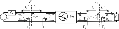
On generator and load sides, in the reference plans P1 and P2, the following expressions are applied respectively:
This definition of ΓS is only valid if the generator has zero amplitude, in other words, it is only the ZS impedance reflection coefficient, by considering a transistor output generator.
The transistors S-parameters are defined:
The different input and output reflection coefficients are detailed in the following sections.
7.4.3.1. Transistor input: Γ1 coefficient
The input reflection coefficient Γ1, which can be written S’11, is a function of transistor S-parameters and load impedance ZL:
[7.4] ![]()
7.4.3.2. Transistor output: Γ2 coefficient
The output reflection coefficient, when the input is closed on the source impedance ZS, is written as an analogy of equation [7.4]:
This reflection coefficient is also sometimes written S’22.
7.4.4. Microwave amplifiers: gain expressions
Different gain expressions exist, transducer gain is the most frequently used for microwaves.
D is defined as:
7.4.4.1. Transducer gain or transducer power gain
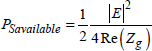
By definition, the transducer gain is the ratio of the power delivered to the load (Pload) to the power available to the source (PSavailable).
The power available to the source is the maximum power that can be delivered to a load. This power is obtained by closing the source on a load equal to. the complex conjugated from its internal impedance, in other words ZS*.
In this case, (PSavailable) becomes equal to:
and the GT expression:
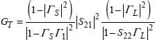
or:
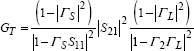
The denominator can also arrange itself to lead to the following expression:
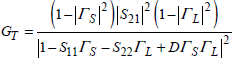
NOTE:- If ZS = ZL = Z0 then ΓS = ΓL = 0 and:
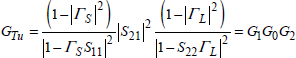
7.4.4.2. Unilateralized transducer gain
If S12 = 0, the transistor is unilateralized. In these conditions, the unilateralized transducer gain is GTu written
7.4.4.3. Maximum available gain (MAG) and Mason gain
This gain, which is only defined when the transistor is stable, is deduced by undertaking a stability study on the transistor.
7.4.5. Unilateralized transistor model: two-port network matching computation
7.4.5.1. Gain computation
As already indicated, the active two-port network is unilateralized when parameter S12 is zero. In reality, S12 is not zero for a transistor but very low because the transistor is an attenuator from access 2 towards access 1.
In these conditions:
Equally:
![]()
The unilateralized transducer gain is given by expression [7.13]:
![]()
[7.13] 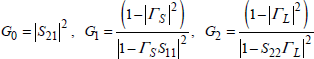
The amplifier can thus be represented by the diagram of Figure 7.15.
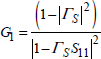
Terms G1 and G2, or the corresponding two-port networks, represent the gain or losses produced by the input and output matching or mismatching.
For example, term G1 affects the matching or mismatching degree of ΓS with S11. Although the two-port network representing G1 is passive, it can give rise to gain superior or inferior to 1. This is possible because of the intrinsic mismatching between Z0 and S11. It is the same for the G2 two-port network.
Figure 7.15. Unilateralized transistor and its input-output two-port network matchings
Expressed in decibels, equation [7.13] becomes:
7.4.5.2. Gain optimization
It is possible to optimize ΓS and ΓL to obtain maximum gains G1 and G2, in this case, GTu will be maximum and:
therefore:
So, the maximum unilateralized transducer gain is equal to:
It can be noted that this expression is identical to the maximum available power gain value GAmax, which corresponds to the same matching conditions.
7.4.5.3. Stability
Since |S11| and |S22| are lower than 1, the unilateralized transistor is unconditionally stable.
7.4.5.4. Constant gain circles
It can be noted that if ΓL = ΓS = 1, then G1 = G2 = 0.
Thus:
The question then asked is: at which point on the Smith chart does the input reflection coefficient ΓS imply a constant gain value G1?
It is defined by the following condition:
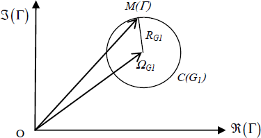
These points correspond to a circle in the complex plan (Figure 7.16), with center RG1 and center ΩGI:
[7.21] ![]()
[7.22] 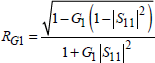
Figure 7.16. Constant gain circle
Particular cases:
– if G1 = 0 (or ΓS = 1), then ΩG1 = 0 = => the circle center is at the Smith chart center and RG1 = 1, corresponds to the external circle of the chart;
– if G1 = 1 (or ΓS = 0), which does not implicate a single two-port network, then:
![]()
– if G1 = G1max (or ΓS = S*11), then: ΩG1 = S*11 and RG1 = 0: this is a point.
Thus for all G1 values such as 0 ≤ G1 ≤ G1max, the circle center is situated on the line passing through the chart center through point S*11.
The circle corresponding to G1 = 1 (or G1 = 0 dB), passes through the chart center.
An example of a circle diagram for a unilateralized transistor is represented on the Smith chart of Figure 7.17.
Figure 7.17. Constant gain and noise circles for a unilateralized transistor
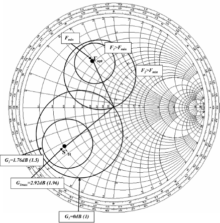
For this transistor, S11 = 0.7∠140°. G1max = 1.96 is obtained.
For G1 = 1, ΩG1 = 0.47∠-140° and RG1 = 0.47.
For G1 = 1.5, ΩG1 = 0.605∠-140° and RG1 = 0.28.
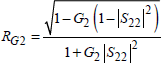
An identical expression group is obtained for the optimization of the output gain G2 two-port network.
In equations [7.21] and [7.22] index 1 must be replaced by index 2:
NOTE:- The gain optimization assumes greater importance at the input, as the best compromise between the amplifier gain and noise figure must be found here, in other words it is necessary to find the optimal source impedance.
7.4.6. Non-unilateralized transistor: general case of a transistor with S12 ≠ 0
As for the unilateralized transistor, the conditions allowing a maximum transducer gain are studied, corresponding to optimal matching conditions, and those assuring amplifier stability.
7.4.6.1. Gain optimization
Not only does the source have to supply a maximum power to the active two-port network, but the load must also receive a maximum power. The transfer gain in power is thus maximum and GTmax.
The conditions to realize this are: ΓS = Γ*1 and ΓL = Γ*2, or equivalently ZS = Z*1 and ZL = Z*2.
Then, the ΓS computation is done by resolving the following equations systems:
The determination of ΓS is given by the resolution of the following second-order equation:
with:
The solution of this second-order equation is thus written:
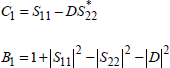
It should be noted that B1 and the quantity under the radical are real, with:
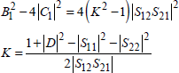
K is the Rollet factor. This factor is a real number. The solution of the second order ΓS equation exists only if the term under the root is positive, in other words if K2 > 1.
Numerous improvements can be made to transistor stability as a function of K values and parameters S11 and S22. A thorough discussion can be found in [ALG 06]. In reality, a circuit designer should work with a perfectly stable transistor, so with K >1.
7.4.7. Low noise amplifier
7.4.7.1. Noise figure optimization: noise circles
An amplifier noise is the sum of input noise (Pne) multiplied by its gain with the intrinsic noise generated by the active component (Pn). The latter is inherent to the technology and so cannot be modified. However, the acquisition of a minimum noise is linked to the input circuit and the presentation of input impedance corresponding to the minimum noise.
Thus designing a minimum noise figure amplifier depends on matching its input for a minimum noise figure and its output for a minimum reflection coefficient.
Amplifier noise factor is given by the following expression:
Noise factor thus uniquely depends on the input impedance and the transistor used:
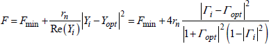
Fmin is a minimum noise factor value, corresponding to an input admittance equal to Yopt, rn is the equivalent resistance of the normalized noise of the component and F is the amplifier noise factor for an input admittance equal to Yi. The input admittance is found on a constant noise circle with the coordinates:
with ![]() ;
;
7.4.7.2. Relations between gain and noise: Friis formula
In the majority of cases, the noise circles are not at the same impedances as the input gain circles, a compromise between the two must thus be made (Figure 7.17).
When several circuits, or stages are cascaded, the Friis formula shows the complete receiver noise factor is largely dependent on the first stage:
It should be noted that the compromise between the gain and noise must be done by considering the whole chain. It can be beneficial to keep a small amount of gain to the detriment of noise at the input if the second stage noise is very high.
7.4.8. General models of low signal microwave amplifiers
Different design configurations are possible for small signal amplifiers in the microwave domain. Only the very general structures are presented by principally differentiating bandwidth.
7.4.8.1. Low bandwidth, single-stage structure
These low bandwidth structures, in the order of 5 to 10%, are often used for low noise amplifier design. The amplifier bandwidth principally depends on the input and output matching circuits of the transistor. Filters are generally used to realize these matchings.
7.4.8.2. Medium bandwidth, numerous-stage structure
These models are bandpass types and obtain a flat gain on a frequency band from 1 to 2 octaves, typically fmax < 2 fmin. Two different structures are principally distinguished:
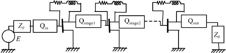
7.4.8.2.1. Non-equilibrated structure: cascaded stages
The problem with this configuration is transistor saturation, which can intervene rapidly, especially as these transistors are designed as low signal transistors. As a result the number of stages is limited to four, or even three.
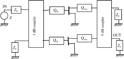
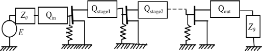
7.4.8.2.2. Balanced structure
The input signal is divided into two or more according to the configurations, in order to limit the transistor saturation phenomenon. At the output, the signals are added together. This topology has the advantage of introducing a natural input and output matching. However, this is at the cost of 3 dB coupler realization.
7.4.8.3. Very wide bandwidth lowpass type
Generally, the minimum frequency is lower than the gigahertz and ratio between the higher frequency and the lower frequency of the bandwidth is above 5. Three principal configurations are distinguished.
7.4.8.3.1. Resistive amplifiers
7.4.8.3.2. Feedback amplifiers
Figure 7.23. Feedback amplifiers
7.4.8.3.3. Distributed amplifiers
In a conventional amplifier, the gain-band product can only be increased by increasing the gain and by placing several cascade stages. A parallel transistor, corresponding to the addition of transconductances, does not resolve the problem as the input and output capacities increase. Matching problems then appear and the gain-band product remains relatively constant.
Figure 7.24. Localized and distributed components distributed amplifiers
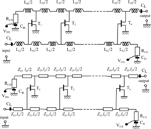
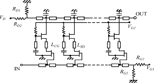
To alleviate this and produce very wideband amplifiers, a distributed or progressive amplifier is designed using a series of identical “distributed” coupling cells along the length of two transmission lines, gate line and drain lines. These two transmission lines can be realized in localized or distributed circuits (Figure 7.24). The principle is the following: each cell can be considered as a controlled voltage source having high input and output impedances. The source generator, situated at the gate line input creates a wave that propagates along the length of this line, which end-loaded by resistance Rg. This wave excites each controlled generator, which in turn creates a wave in the drain line.
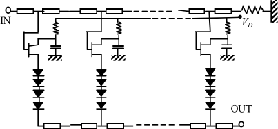
The gate and drain lines constitute the amplifier matching components by compensating the transistor input and output internal capacities by the inductances. As an example, the values of the components of Figure 7.25 are:

The low cutoff frequency is limited by biasing components (CL capacities). This configuration is used for optical receivers for very high data rates (12, 40, and 80 Gb/s) communications.
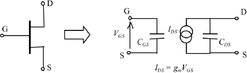
Figure 7.25. High frequency FET simplified equivalent electrical circuit
Since the presentation of the first distributed amplifier (Figure 7.24), numerous improvements have been proposed to increase gain or bandwidth. These improvements are recalled bellow [RUM 04c]:
– design of distributed amplifiers with very high frequency field effect or heterojunction bipolar transistors. Bandwidths of 80 GHz have been obtained with InP/InGaAs HFET transistors;
– single transistor replacement by cascode structure. This mounting type increases gain but the output impedance becomes negative at high frequencies. This can introduce loss compensations, but mainly brings high-frequency instabilities, which forces the addition of resistance in the gate of the second transistor of the cascode stage;
– placement of a series capacitance in front of the first transistor. As a result, the gate line is comprised of these parallel transistor Cgs capacities and inductances or line sections in series. Increasing capacitance leads to inductance increases and decreasing line cutoff frequencies. The series capacitance allows the increases of the gate line cutoff frequency;
– addition of inductance in the gate of the second transistor and series inductance between the drain of the first transistor and the source of the second transistor. The simulations show a bandwidth increase [KIM 96a];
– coupling of several distributed amplifier stages by using a matrix structure. This arrangement increases the gain but at the cost of circuit component complexity;
– introduction of active loads in the gate biasing circuit, in order to decrease to very low frequencies.