Chapter 8
Optics and Optronics
“Optics rule: everything seen from a distance look larger”
Extract from Nouvelles pensées échevelées,
Stanislaw Jerzy Lec (1909–1966)
8.1. Overview
We discuss the “physical layer” of wireless optical terminals in this chapter. The digital communication part and the communication protocol part will be discussed in Chapter 10 (OSI layers 1 and 2 and the TCP/IP layer 1).
The other layers are application oriented and will not be considered in this book.
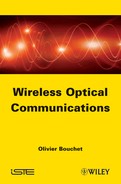
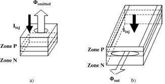
The different modules of a wireless optical terminal are illustrated in Figures 8.1 and 8.2.
8.2. Optronics: transmitters and receivers
8.2.1. Overviews on materials and structures
The transmitter and receiver components of this section are components of very small dimensions (volumes below 1 mm3) processed by deposition of thin films on semiconductor materials.
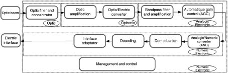
A crystal of semiconductor material is a poor conductor. The electrons which are the charge carriers are not free to move within the material when they occupy energy states in the low-energy valence band. They can only contribute to the current flow when they get enough energy in excess of the bandgap and are free in the conduction band as shown in Figure 8.3.
Figure 8.1. Diagram of an optical wireless transmitter
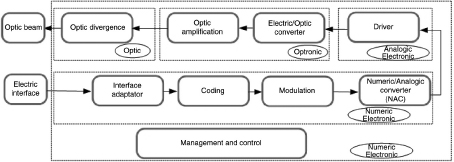
Figure 8.2. Diagram of an optical wireless receiver
This excess in energy needed to gain kinetic energy and be admitted into the conduction band may be the result of several physical phenomena, such as:
– an increase in temperature of a few K generally considered as a “parasitic phenomenon” (leakage current drifts depend on temperature variations, etc.);
– the presence of light quanta, photons, whose energies depend on their colors, in other words their frequencies, the wavelengths in vacuum, and the values of their energies compared to the bandgap energy.
It must be noted that when an electron from the valence band is well accepted in the conduction band, it releases its original condition and yields a positive hole charge carrier, which is also free to move. Thus far when the energy of an incident photon is greater than the energy gap Eg, it gives rise to an electron–hole pair when the photon is absorbed inside the semiconductor material.
Figure 8.3. Band diagram of a crystal of semiconductor material
The condition on the frequency and wavelength is given by (equation [8.1]):
Equation 8.1. Cutoff wavelength
Next to the notion of electron–hole pair, we must introduce the notion of lifetime. An electron of the conduction band may be solicited to lose part of its energy, or take a state occupied by a hole in the valence band. The electron loses then a quantum of energy, may either find itself trapped on a level of impurity or defect in the crystal, or recombines with a hole when losing a quantum of energy at least equal to Eg.
In some semiconductor materials to which we will soon come back, the loss of this quantum of energy can result in the emission of a photon whose wavelength in vacuum is given by the following relations:
The crystals of semiconductor materials are assemblies of one or more different atoms according to geometric rules in space which are also different. The physical properties and in particular the optical and electrical properties can be very different between materials. For example, looking at columns III and V of the Mendeleev’s table, when we compare silicon (Si) and arsenic (As), gallium (Ga), phosphorus (P), indium (In), and aluminum (Al) compounds, we discover that the probabilities of radiative electron transitions between conduction band and valence band are very different. These transitions “conduction band valley-to-valence band summit” are indirect in the case of silicon and consequently unlikely, compared to the direct transitions, and therefore very likely in the case of the semiconductor “III–V” compounds. Energy gaps and valence–conduction band shapes of the III–V compounds lead to very different spectral properties, the spectrum of visible to near- infrared spectral range of fiber optic transmission telecommunications.
The semiconductor sources of the light waves detected by silicon photodiodes in the visible to near-infrared spectral range (0.4–1 μm wavelength) are widespread in the market of optoelectronic components and devices. The industrial development of sources and detectors operating in the infrared spectral range from “1 to 1.6 microns” for “Fibre To The Home (FTTH)” applications is still undergoing a high growth rate.
8.2.2. Light sources
Most of the sources made from semiconductor materials have the following advantages:
– their size, as we have previously mentioned a few mm3 deposited on the bases of a few mm2;
– the near field of the exit pupil and the radiation pattern: well-known, stable, and reproducible;
– the possibility for modulating the flow of energy and the optical frequency power spectrum directly by the injection current: we can reach several tens of gigahertz, frequency dependent of the internal structure of the component.
Their structures are junctions elaborated by deposition of thin layers of III–V compounds (a few hundred nanometers to several microns thick) on a GaAs or InP. Radiative transitions and spontaneous emission occur in the junction area of these diodes when a forward injection current is applied. The spontaneous emission spectra depend on the III–V compound band structures and the gap energy which depend themselves on the chemical compositions of the compounds.
We will see later on in this section the different operating modes and optical behavior of these light sources.
8.2.2.1. Light-emitting diodes (LEDs) and spontaneous emission
Electrons and holes injected into the junction will fill the energy levels in the bottom of the conduction band and the top of the valence band, respectively. These two types of carriers will be required to recombine by emitting photons whose energies are quite different. Therefore, the spectral width of the emission will be quite large.
The “output radiant power vs injected current” curve is approximately linear up to a few milliwatts per square mm, limited by the heat dissipation of the junction.
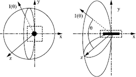
Two junction structures lead to two types of exit pupil and radiation pattern:
The top surface-emitting diodes (Figure 8.4(a)): There are no plans to impose the directions of propagation of photons emitted inside the “chip”; the diameter of the pupil is the same as the opening of the upper contact surface; the radiation pattern is said to be Lambert’s law (sphere of revolution around the z-axis), sphere tangent to the surface (Figure 8.5(a)).
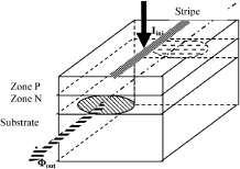
The edge-emitting diodes (Figure 8.4(b)): The current is injected through an electrode — ribbon through a light guides between the two sides of the emissive “chip” (Figure 8.5(b) — the index n in the (x, z) is different from that in the (y, z)).
Figure 8.4. LED spontaneous emission structures
These two sets of structures from industrially mature technologies are very reliable. Both are designed and built to transmit near-infrared waves and are used in many electronic and optical applications (remote controls, emission in the optical fiber links, etc.). Costs are moderate due to the volume of the market.
Figure 8.5. Lambert’s law: (a) I(θ) = I(0).cos θ and (b) I(θ) = I(0).(cosθ)n
The following section is entirely devoted to surface emitting white light LEDs. The optical energy is distributed in the visible region from 380 nm to 780 nm. Their first applications are lighting and signalization.
8.2.2.2. White LEDs or visible light communication (VLC) LED
New LED structures, usually in SMC configuration (surface mounting components), have emerged since the 1990s. They aim to replace, over time, fluorescent or incandescent light sources. These new generations of LEDs provide a light output greater than that of an incandescent lamp and a performance/cost ratio (ability of light and life) that approximates more and more preferably the fluorescent tubes. In addition, technical progress in order to obtain ever more powerful LEDs, with warmer colors, and higher yields.
White LEDs are devices currently planned for lighting, but it is possible to modulate the intensity with relatively short switching times. The switching time is the time required to grow from a current of 10% to 90% of its final value or decreases from 90% to 10% and it depends on the capacity of the junction in the diode. This feature allows data rates relatively high in digital data transmission by optical fibers, for example. They have, in this regard, a number of advantages, including being powered by the industry and we can imagine a coupling between data transmission over power line and wireless optical transmission.
There are two main types of white LEDs:
– The first one is made of three LED colors: red, green, and blue (Figure 8.6). This light source is called multi-chip white LED or RGB LED. By modulating the intensity of one or more color, it is possible to achieve an optical digital transmission with higher data rates. However, the simultaneous operation of these LEDs can be tricky and the aging of each different color can degrade the quality of white light.
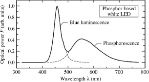
– The second approach is more recent. A layer of fluorescent material is deposited over a blue LED. This layer emits yellow light when excited by the blue light LED (Figure 8.7). The mixture of blue and yellow light creates an almost white light. For data communication, the blue wavelength is used because of its short switching time. To avoid the bluish appearance, changes are implemented, such as blue LED combined with a multi-phosphors or UV (ultraviolet) LED with phosphors RGB (red, green, and blue).
Figure 8.6. Multi-chip LED spectra
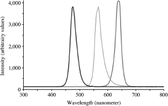
Figure 8.7. Phosphor-coated LED spectra
8.2.2.3. The semiconductor laser structure
The first amplification by stimulated emission structures developed on substrates of semiconductor materials was proposed by Professor Aigrain in 1958 and completed in 1962. Based on the calculations of Albert Einstein, the population inversion, which contradicts the thermodynamic equilibrium between energy levels and leads to the phenomenon of amplification, can be achieved by a strong injection of carriers in the conduction and valence bands.
Going back to the structure of LED emitting “edge-on”. They consist of a heterojunction — epitaxial thin films of III–V materials with different compositions — which comes in the form of a planar dielectric waveguide with rectangular section. The carriers injected by the contact strip recombine radiatively in the contact and within the guide along which the photons created can spread. When the injected current density is high enough, there is inversion of the populations and the effect of gain occurs as it can be seen on the output radiant power versus the injected current curve. The diode becomes super-luminescent, high brightness, and the spectrum of the transmitted wave is narrower.
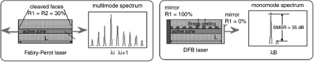
In the case of “Fabry–Perot” lasers (Figure 8.8), the waveguide is limited by two reflective facets cleaved along two parallel crystal planes and operates as a resonant cavity. In the case of single-mode distributed feedback lasers, the resonance can be obtained along a Bragg grating (periodic corrugation along the waveguide axis), a grating whose function is to select a single spatiotemporal mode.
Figure 8.8. Laser structure: thin epitaxial layers, stripe and Fabry–Perot resonator
When the injection current I is sufficiently high and exceeds the threshold current, the gain is almost equal to the total losses of the cavity which are the propagation losses of the guide (diffusion, absorption, defects at the interfaces between epitaxial thin films, etc.) and losses at the level of reflective facets of the resonator.
Thus, in general, the active portion of semiconductor lasers has a dielectric waveguide structure buried in thin layers of materials of different compositions and electronic and optical properties. Unlike the LED spontaneous emission, the laser is an amplifier/generator of monochromatic light waves (low spectral width), consistent (the photons are in phase), with highly directional exit pupils from a few microns square. They are structurally more complex than emission LED with a level of modulation speed, power, and higher performance, but also a higher cost.
There is a second type of laser structure called vertical external cavity surface emitting laser (VCSEL) — a laser emission from the surface with a resonant cavity and amplifier composed of vertical Bragg mirrors. The VCSEL is cheaper than the structures emitting laser facets cleaved. Its radiation pattern is of a revolution, the circular exit pupil, its power consumption, and output radiant power are all lower.
8.2.2.4. Synthesis
When we look for the optimal solution, we must take into account the following: either high transmission power, fast modulation, divergence large enough to cover an important area or more transmitting device and security Class 1.
The electrical/optical converter is usually the association of a laser power driver and an automatic transmit power control. This device performs an operation against amplification loop feedback for controlling the signal to be transmitted with sufficient power to allow a correct reception.
The main element of the transmission system is the optical source. Most systems use laser diodes (LDs) due to their speed of response and radiant power output. The optical power can be increased by inserting an optical fiber amplifier-type erbium-doped fiber amplifiers (EDFAs), but the cost and congestion currently limit this option. The infrared LED light sources are also considerations in the implementation of optical links. In addition, there is a growing interest in the use of LEDs in the visible range, with a dual function that would be obvious and advantageous to provide an efficient lighting in semiconductors and optical communications to achieve [TAN 00].
Table 8.1 shows the different comparative characteristics of the LED and the LD.
Table 8.1. Comparative LED–LD
| Parameters | LED | LD |
| Spectral width | 25–100 nm (10–50 THz) | <10−5 to 5 nm (<1 MHz to 2 MHz) |
| Baseband modulation | Tens of kHz to tens of MHz | Tens of MHz to tens of GHz |
| E/O efficiency | 10–20% | 30–70% |
| Cost | Low | Low to moderate |
For a significant energy flow, it is possible to use one or more lasers, coupled or not with doped fiber amplifiers (power increase), and one or more diffusers (homogeneous distribution of the transmission power). The realization of this configuration seems easier in the spectral window at 1,550 nm because the elements offer this level of power are commercially available.
8.2.3. Optronics receivers
Because of their small size, the optronic receiving devices are essentially junctions called photodetector photodiodes (PD), and three main parameters determine the choice in an optical wireless system:
– The response time of a photodiode is characterized by its rise or fall time, the latter being longer. Generally, the time required to reach 90% of the final current of the photodiode. The response time value is important in selecting a photodiode, when this value is low the photodiode detects modulation frequencies more quickly, but its active surface is smaller.
– The sensitivity is the second parameter defined as the minimum received optical power for a correct detection of the transmitted signal. The value of the sensitivity is involved in the selection but it is best to consider the sensitivity of the complete optical reception (see Chapter 6).
– The receiver sensitive and active area is directly proportional to the cosine of the field of view and inversely proportional to the response time.
It is possible to distinguish four main groups: the photovoltaic cell, the PIN photodiode, the avalanche photodiode (APD), and the metal–semiconductor–metal (MSM) photodiode.
8.2.3.1. Photovoltaic cells
A photovoltaic cell is the most basic electronic semiconductor component that operates as a battery, produces a current proportional to the incident light when connected to a short circuit. The electron–hole pairs created by the photon absorption are dissociated by the permanent electric field through the space charge region at the P–N junction (positive–negative), interface between the P- and N-doped layers. In addition, in the case of the binary, ternary, and quaternary III–V compounds, the energy gap of the semiconductor can be matched with the photon energy (Figure 8.10).
Figure 8.10. Photovoltaic cell
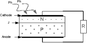
Specifically, the top layer of the cell is an N-doped layer whose electron density is very high and thin to let the largest number of photons get through into the junction. The bottom layer of the cell is a P-doped layer whose hole density is very high.
Under the internal electric field action, the free electrons and holes are swept out of the junction area and a space charge area develops around the junction plane. As represented in Figure 8.10, a conductive thin film covers the upper surface (type N: cathode) of the chip to allow the passage of photons. The underside of the opposite chip is deposited on p-type electrode (anode).
The photovoltaic cell can be considered as the combination of an electric generator and a diode. We can add multiple layers and junctions in order to optimize the energy spectrum of photons. We obtain multijunction cells.
This light sensor is not the most suitable modulated signal receiver because its response time is high, in the order of milliseconds. It can be used as an energy resource. The current yields of around 20% are likely to evolve rapidly.
8.2.3.2. PIN photodiode
The PIN photodiode is a multilayer structure (basically three layers), the intrinsic I-layer between P-doped and N-doped layers. Under a reverse bias, it operates as a current source, the absorption of photons creates electron–hole pairs which are separated under the high biasing electric field and recombine to provide the photoelectric current. This current has an amplitude proportional to the radiant optical power incident on the active surface.
In general, this settled in the junction of the photodiode reverse current (equation [8.3]), expression (see Chapter 6):
Equation 8.3. Current of the photodiode
where
– id is the dark current.
– is = R.P photocurrent proportional to the incident radiant power P.
– R is the responsivity.
The photodiode has a responsivity that depends on the semiconductor material and furthermore on the incident signal optical spectrum (Figure 8.11).
Figure 8.11. Responsivity versus wavelength
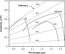
Material example and sensitivity band:
– Silicon (Si): 400–1,000 nm;
– Germanium (Ge): 800–1,600 nm;
– Indium callium arsenide (InGaAs): 800–1,800 nm.
The PIN photodiodes are widely used due to their proper responsivity, their good tolerance to temperature variations and the low bias voltage. The response time and the active surface are suitable for moderate bandwidth optical wireless communications.
8.2.3.3. Avalanche photodiode
Under high voltage reverse bias, below breakdown, the P–N junction may operate in the avalanche mode with internal multiplication gain. The radiant power of the amplitude-modulated incident signal is often very low; it may be appropriate to amplify the photocurrent. The principle is a chain ionization by impact of the carriers under the influence of an electric field much more intense than that of a PIN photodiode. Each high-energy primary carrier will therefore release several secondary carriers from their ions. The multiplication gain M can be derived from the following equation:
In the following expression of the signal/noise power, assuming for simplicity that the quantum noise emission is negligible compared to other sources of noise, we consider the two terms in the denominator:
![]()
where
– e is the electron charge.
– k is the Boltzmann constant.
– T is the temperature in Kelvin.
– Pincident is the incident optical radiant power.
– Rload is the load resistance of the diode.
– The radiofrequency bandwidth and the multiplication factor are, respectively, represented by the letters B and M.
– R is the intrinsic responsivity of the detector at unity multiplication gain.
In the case of transmissions at high data rates, looking into the denominator, we have the possibility to adjust the gain by adjusting the reverse bias voltage applied so that the first noise term becomes equal to the second thermal noise term.
8.2.3.4. Metal–semiconductor–metal (MSM) structure
The MSM structure can also provide improved detection performance by the possibility of obtaining a large active surface with a very low response time and easy implementation. These photodiodes have been the subject of study [TEM 96], due to a simple and compact structure facilitated by a monolithic integration of field effect transistors. Indeed, the sensitivity of the detectors is inversely proportional to the response time which is directly proportional to the capacitive effect of the active surface detection. The MSM detector could be optimized on the basis of a low capacitance per unit area. Experiments have shown beneficial first results [OBR 05] but further studies are needed in this direction.
8.3. Optics
8.3.1. Transmitter optical device
The problem of optical emission in limited space is the following: how can we obtain simultaneously a significant divergence of the transmitted beam (typically ±45° or 90°) and keep a Safety Class 1 with an acceptable radiant power attenuation and a low-volume optical device?
As far as optical emission in free space is concerned, the constraint is less important and can be summarized as follows: by what means can we get a low divergence of the emitted beam, typically a few milliradians, while in a Safety Class 1 with an optical acceptable budget and reduced volume of the device?
The resolution of this problem is based on two main parameters (Figure 8.12): the distance, called focal distance (D) between the emission source (Opt) and the combination of lenses and/or mirrors, and the characteristics of these lenses and mirrors (diameter, radius, etc.).
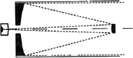
In free-space optics, several solutions are possible, a small Cassegrain telescope with a combination of diverging lens and diffuser. The first solution is the use of multiple mirrors (Cassegrain telescope). The Cassegrain telescope (Figure 8.13) consists of two mirrors: a concave and parabolic mirror (called primary) and a hyperbolic convex mirror (called secondary). The main advantage of the Cassegrain is its low cost and its limited divergence.
Figure 8.12. Optical emission
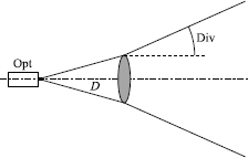
Figure 8.13. Cassegrain telescope
8.3.2. Receiver optical device
The problem of propagation in limited as well as in free space at the receiver level can also be summarized by one question: what must we do to obtain a high concentration of the transmitted beam in a solid angle as large as possible, typically ±45° or 90°, while avoiding defocusing with an acceptable optical budget through a low-volume optical device, knowing that beyond an angular limit, the incident beam does not reach perpendicularly the active surface of the photodiode?
As far as propagation in free space is concerned, the solution depends on three main parameters: the distance, called focal distance (D) between the combination of lenses and/or mirrors (with their special characteristics) and the photodiode, the characteristics of these lenses or mirrors (diameter, radius, etc.), and the active surface of the photodiode.
Without going back to the calculation mentioned in Chapter 6, it is nevertheless possible to consider several solutions from the Cassegrain telescope to the fish-eye lenses.
In the field of optics in free space, the first solution is a combination of mirrors. As mentioned above, the Cassegrain telescope (Figure 8.13) consists of two mirrors: a concave parabolic (primary) and a convex (secondary) mirror. The main advantage of the Cassegrain telescope is its low cost with a gain (area ratio) and the large field of view is limited to receiving, but the secondary support mirror can cause a very damaging gray area.
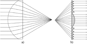
In the field of optics in limited space, the first solution is based on a spherical lens. In the research for a signal collection while limiting the length of the device, it is necessary to obtain a ratio of diameter of the lens/focal length as high as possible, but to avoid that, the focus point will move away from the optical axis; it is essential to find a good compromise between the size of the collector surface and a short focal length.
We must therefore move toward a lens as large as possible with the shortest possible focal length. Now, shorter the focus, more the radius of curvature approaches the diameter of the lens, the lens tends to a hemisphere. But to limit spherical aberrations inherent to conventional spherical lenses, we should choose an aspherical lens (Figure 8.15(a)) with a refractive index n. With this approach, the size is smaller with a larger field of view, but due to the thickness of the lens, the absorption signal is more important and its gain is lower (about 3 dB). This approach remains the most usual.
Compared to the problem of thick aspherical lenses, Fresnel lenses are a good alternative. The Fresnel lens (Figure 8.15(b)) is a special type of lens invented by Augustin-Jean Fresnel. Its design allows the achievement of the large field of view with a short focal length, a reduced weight and volume compared to the implementation of conventional lens.
Figure 8.15. Example of aspherical lens (a) and Fresnel (b)
In the case of focusing by a Fresnel lens, the area considered is that of the lens also weighted by the recovery of surfaces of the focal spot and the detector surface. The gain is proportional to the ratio of surfaces and a Fresnel lens is not fundamentally different from a conventional lens, except that it is done for a specific wavelength. Fresnel lenses can produce optical devices especially at lower costs (less material is needed) and with a smaller size. Limited divergence and the problem of the orientation of these devices, however, remain the same as that encountered with conventional lenses.
Another possibility is to increase the reception sensitivity using an optic amplifier concentrator or “fireball” [MIH 07]. That is to say, a photomultiplier with microspheres from a part of the energy received, with an adjustable amplification. But this is currently experimental.
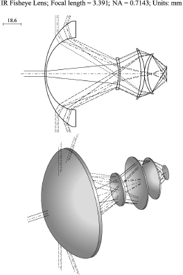
Still with the aim to capture the maximum of the incident optical beam with great freedom of incident angle, we should mention the combination of lens for forming the Maxwell “fisheye” [MAX 54]. The “fisheye” device (Figure 8.16) is a lens with an important refractive index to mimic the characteristics of a fish eye and get a wide field of view with defocus limited sensitivity. The size and cost of such a device remains a point to be refined. A combination of “fisheye” and “cat eye” lens provides superior performance in optical terms [ALH 06].
Each solution has advantages and disadvantages and a phase of economic materials integration is essential to reduce the cost and the volume.
It must be remembered that an increase in the field of view also leads to an increase in the optical noise and possible interference. Optical filtering is required to reduce this noise. There are different techniques: the spatial filter (diaphragm) or wavelength filter (attenuator). These are discussed below.
Figure 8.16. Fisheye lens [ALH 06]
8.3.3. Optical filtering
8.3.3.1. Spatial filter or diaphragm
The spatial filter (or diaphragm) is a thin screen with an aperture in its center. The role of this diaphragm is to restrict part of the optical beam to limit the optical noise and avoid saturation of the receiving device. The saturation of the optical detector may be avoided using feedback control of the aperture of this diaphragm. Other electronic solutions are possible such as automatic mitigation (automatic attenuation control — AAC) or automatic gain control (AGC).
8.3.3.2. Wavelength filters or attenuators
Ambient light is the largest source of interference or noise and may affect an optical link (see Chapter 4). It induces a constant current on the photodetector of the receiving optical system and can be treated by the electric part of the receiving system [PHA 98].
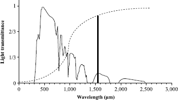
However, different studies on this subject have been undertaken and the most relevant seems the addition of an optical filter to reject background radiation out of band signal, thereby reducing the incident radiant power level (Figure 8.17). Two main types of filters are presented:
– Absorption by an optical filter can reject particular ambient light and the Sun. It has a wide field of view (theoretically independent of the incident angle) and a filter typically of several hundred nanometers (broadband spectrum). It is possible to appropriately filter by the incorporation of specific layers directly on the photoelectric detector [OBR 00]. The use of a holographic diffuser also allows any filtering of ambient light [JIV 01]. These absorption filters allow us to have band-pass, high-pass, or low-pass filters. Figure 8.17 shows an example of high-pass filter (dashed line) to absorb some solar radiation (black line) while letting the wavelength of the incident beam (bold line at 1,550 nm).
Figure 8.17. Example of optical high-pass filtering
– Interference filters are band-pass filters. They consist of multiple layers and are much more effective in filtering accuracy of the order of several nanometers. These filters are sensitive to the angle of incidence of the beam (shift of the wavelength of about 1 nm per degree) and are most often used for beams at normal incidence because there is a loss of signal in terms of power as in a departure from normal incidence. Fabry–Perot filters, for example, are tunable in wavelength according to the angle of incidence. This should also include Bragg mirrors and Fabry–Perot vertical cavities based also on the interference. Experimental systems have circumvented this problem in terms of sensitivity by sticking a soft interference filter on the curved surface of a hemispherical lens [KAH 95]. This maintains the narrow spectral window while increasing the field of view but the cost of implementation is high. The latter filter is close to the ideal filter for a wireless optic reception, e.g. a very narrow band-pass filter insensitive to the angle of incidence and with a large field of view.
8.3.4. Summary
The search for the optimal solution is defined by the following elements: high-sensitivity receiver, fast response time, and large active surface. The optimal solution is coupled with the optical device which must provide a high concentration for a maximal equivalent surface and a good reception with a large field of view.
Generally, the optical/electrical converter is associated with one or several low-noise amplifiers (TIA — transimpedance amplifier) which increase the received signal and possibly a receiver automatic control gain (AGC or ACG). This command performs an amplification operation with a feedback loop to control the received signal at a level high enough to allow for proper treatment while avoiding saturation.
Other more exploratory tracks can also be considered, such as:
– Fresnel lens in three dimensions in order to increase the field of view;
– nanophotonics for an optimized compactness of the receiver.
Finally, this section shows that the receiving device depends not only on the receiving optronic device but also on the optical device characteristics and must be a compromise between performance, compactness, and cost. This choice also depends on the type of treatment that is performed on the electrical signal. This point is developed in the next chapter (Chapter 9).