
7
DIFFERENTIAL SIGNALING
7.1 Removal of Common-Mode Noise
7.2 Differential Crosstalk
7.3 Virtual Reference Plane
7.4 Propagation of Modal Voltages
7.5 Common Terminology
7.6 Drawbacks of Differential Signaling
7.6.1 Mode Conversion
7.6.2 Fiber-Weave Effect
References
Problems
When the interconnections between drivers and receivers on a bus are implemented with a dedicated transmission line for each bit, the signaling scheme is said to be single ended. Buses designed with single-ended signaling generally work well up to approximately 1 to 2 Gb/s. As data rates increase, it becomes increasingly difficult to maintain adequate signal integrity because digital systems are notoriously noisy. For example, large arrays of I/O circuits used to drive digital information onto the bus induce noise on the power and ground planes called simultaneous switching noise (for a complete description, see a book by Hall et al. [2000]). There are many other sources of noise that can severely distort the integrity of the digital waveform such as crosstalk (as discussed in Chapter 4) and nonideal current return paths (as discussed in Chapter 10). With single-ended signaling, each data bit is transmitted on a single transmission line and latched into the receiver with the bus clock. The decision of whether the bit is a 0 or a 1 is determined by comparing the received waveform to a reference voltage vref. If the received waveform has a voltage greater than vref, the signal is latched in as a 1, and if it is below vref, it is latched in as a logic 0. Noise coupled onto the driver, receiver, transmission lines, reference planes, or clock circuits will degrade the ideal relationship between the transmitted waveform and uref. If the magnitude of the noise is large enough, the incorrect digital states will be latched into the receiver, and bit errors will occur. Figure 7-1 depicts how noise can make the determination of a logic 0 or 1 uncertain.
Figure 7-1 How system noise can severely degrade signal integrity on single-ended buses. The ideal versus noisy receiver voltages compared to the reference voltage.

Figure 7-2 Differential signaling where each bit is transmitted from the driver to a receiver using a pair of transmission lines driven in the odd mode. The signal is recovered at the receiver with a differential amplifier.
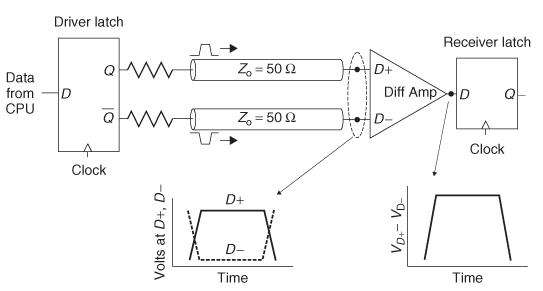
A strategy that reduces the effect of the system noise dramatically is to dedicate a pair of transmission lines for each bit on the bus. The two transmission lines are driven 180° out of phase (in the odd mode), and the differences between the voltages are used to recover the signal at the receiver using a differential amplifier. This technique is called differential signaling and is depicted in Figure 7-2.
7.1 REMOVAL OF COMMON-MODE NOISE
Differential signaling is very effective for removing common-mode noise, which is defined as noise present on both legs of the differential pair. If the bus is designed properly so that the legs of the differential pairs are in close proximity to each other, the noise on D+ will be approximately equal to the noise on D-. Therefore, assuming that the receiver’s differential amplifier has a reasonable common-mode rejection ratio, the noise will be eliminated. For example, assume that there is noise with a magnitude of vnoise coupled equally onto both legs of a differential pair. The output of a differential amplifier with unity gain is
which removes the common-mode noise.
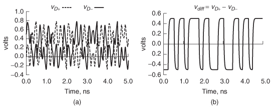
Figure 7-3 shows an example of a differential interconnect with noise present on the ground plane (vnoise). In this case, the noise is common to both legs of the driver. Figure 7-4a shows a simulated stream of data bits at the input to a differential amplifier with significant common-mode noise. Note that the digital state of the single-ended waveforms VD+ and VD– is indeterminable because the noise is so large. However, since the noise is common mode, the bit stream can be recovered when the signals are subtracted by a differential amplifier (VD+ – VD–), as shown in Figure 7-4b.
Figure 7-3 Differential driver and interconnect with common-mode noise present on the ground. Noise on both the power and ground planes is very common in digital designs.
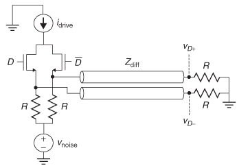
Figure 7-4 Example of how common-mode noise is eliminated with differential signal-ing: (a) single-ended waveforms at each leg of a differential receiver showing commonmode noise; (b) differential waveform.
7.2 DIFFERENTIAL CROSSTALK
Although crosstalk noise on a differential pair has a significant common-mode component, it also has a differential component because the distance between an aggressor and each side of the pair differs (in some cases, if the aggressor is on another layer, the crosstalk could be 100% common mode, but this is rare). Consequently, each leg will experience slightly different crosstalk, which will not be rejected by the differential amplifier. Nonetheless, under certain conditions, differential signaling can reduce crosstalk significantly.
If the crosstalk between single-ended lines is compared to the crosstalk between differential pairs, the differential crosstalk will be less if the spacing is similar. The drawback is that the differential pair will occupy significantly more board area. Additionally, if the single-ended pairs are spaced far enough apart so that the same board area as the differential pairs is occupied, the single-ended crosstalk is typically lower simply because the signals are spaced so far apart. For example, consider Figure 7-5, which shows three cases:
1. Two single-ended coupled transmission lines spaced 10 mils apart (Figure 7-5a).
2. Two differential pairs with an interpair spacing of 10 mils (Figure 7-5b). Note that the spacing between pairs is identical to the spacing between single-ended signals in case 1.
3. Two single-ended coupled transmission lines spaced 28 mils apart (Figure 7-5c), which occupies the same board area as the differential pairs of case 2.
Figure 7-6 shows the far end crosstalk for each case when the aggressors are driven with 100-ps-wide pulses and line voltages of 0.5 V. The differential crosstalk is calculated as the difference between V + and V–:
![]()
Figure 7-5 Cross sections used to compare differential versus single-ended crosstalk: (a) two single-ended signals; (b) two differential pairs with the same pair spacing as that of the single-ended signals in (a); (c) two widely spaced single-ended signals that occupy the same board area as the differential pairs (dimensions in mils).

Figure 7-6 Crosstalk for the cross sections in Figure 7-5 demonstrating that differential signaling does not reduce crosstalk compared to single-ended signaling if the same board area is used. However, if the spacing between differential pairs is similar to the spacing between single-ended signals, crosstalk in reduced (5-in. microstrip).

Note that the differential crosstalk (case 2) is less than the identically spaced single-ended crosstalk (case 1), but greater than a single-ended case that occupies the same board space as two differential pairs (case 3). This scenario is typical for modern printed circuit boards, but is not necessarily always true. The benefit of differential signaling for crosstalk is dependent on the specific geometries and dielectric properties of the design.
7.3 VIRTUAL REFERENCE PLANE
Another advantage of differential signaling is that the complementary nature of the electric and magnetic fields creates a virtual reference plane that provides a continuous return path for the current. Figure 7-7 shows the field patterns for a differential pair driven in the odd mode. Note that halfway between the conductors there exists a plane that is normal to the electric fields and tangent to the magnetic fields. These conditions are consistent with Section 3.2.1, which describes the boundary conditions of a perfectly conducting plane. Therefore, for a differential pair, there exists a virtual reference plane between the conductors. The existence of the virtual reference plane is extremely helpful for cases when a nonideal reference exists that helps preserve signal integrity. Some common examples of a nonideal reference include connector transitions, via fields, layer transitions, and routing over a slot in the reference plane. In Chapter 10 we describe in detail the ill effects of nonideal reference planes. Additionally, when the fields are confined between the conductors (i.e., strongly coupled to the virtual reference plane), they are less apt to fringe out to other signals, which helps reduce crosstalk.
Figure 7-7 For an odd-mode (or differential) signal, the fields orient so that an ideal virtual reference plane existed between the conductors. When the physical plane is interrupted, the virtual plane provides a continuous reference for a differential signal and helps preserve signal integrity.

7.4 PROPAGATION OF MODAL VOLTAGES
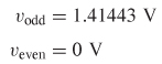
For a multiconductor system, in Chapter 4 we discussed how all digital signal states are composed of linear combinations of the modal voltages. For a single differential pair, the two modes are the even and odd modes. Ideally, the differential pair is driven with lines 1 and 2 180° out of phase so that all of the energy is contained solely in the odd mode. However, if common-mode noise is coupled onto the differential pair, some energy will exist simultaneously in the even mode. This is easy to show mathematically using modal analysis, as discussed in Section 4.4. For example, consider a differential pair with line voltages VD+ and VD–, which are composed of linear combinations of the oddand even-mode voltages:

where [TV] is a matrix containing the eigenvectors of the product LC as developed in Section 4.4.1.
If the differential pair is driven exactly 180° out of phase and there is no noise present, the oddand even-mode voltages are calculated, where
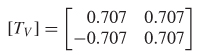
from Example 4-4:

resulting in
which proves that all the energy is contained on the odd mode.
However, if common-mode noise is present, energy is introduced into the even mode. If vnoise is the voltage noise introduced to each leg of the pair, the even and odd modes are calculated:
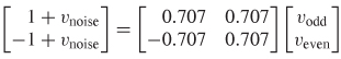
Therefore, the common-mode noise propagates in the even mode
The voltage present on each leg of the differential pair can be calculated from the modal voltages by solving (7-2):

In a differential bus, the line voltages are subtracted with a differential amplifier at the receiver which eliminates the noise.
![]()
To summarize, a differential signaling scheme eliminates energy in the even mode.
7.5 COMMON TERMINOLOGY
For systems with more than two signal conductors, the terms even mode and odd mode are no longer applicable. When analyzing differential buses, it is common to refer to a pair being driven with two signals 180° out of phase as the differential mode and two signals driven in phase as the common mode. The differentialand common-mode terms are simply naming conventions and are not technically modes at all. Analysis of the modal voltages propagating on multiconductor systems as described in Section 4.4 will show that the digital states do not correspond directly to modal voltages for systems with more than two signal conductors.
The differential-mode impedance is defined as twice the odd mode, and the common-mode impedance is one-half the even mode. The oddand even-mode impedance values are described in Section 4.3.1.
It should be noted that equations (7-5a) and (7-5b) are typically used for the purpose of specifying design guidelines. The actual impedance of a differential pair may not correspond directly to Zdifferential if there is significant coupling to adjacent pairs. Equations (7-5a) and (7-5b) are representative of the true pair impedance values only if the interpair coupling is weak. Remember: In a multiconductor system with N signal conductors, there will be N unique modal impedance values.
It is also true that for a system with N signal conductors, there will be N modal propagation velocities. If the transmission lines are routed in a homogeneous dielectric (such as a stripline), all the modal velocities will be identical. However, for a nonhomogeneous dielectric (such as a microstrip), the differentialand common-mode propagation velocities are approximately equal to the oddand even-mode velocities if the interpair coupling is weak. Oddand even-mode velocities are defined in Section 4.3.1:
To quantify the voltage propagating in the differential and common modes, the following definitions are often used:

where vdm is the voltage propagating in the differential mode, vcm is the voltage propagating in the common mode, V represents the voltage propagating on line 1 (the same as VD+ used in the two-signal-conductor example), and ![]() represents the complementary signal propagating on line 2 (VD– used in the two-signal-conductor example).
represents the complementary signal propagating on line 2 (VD– used in the two-signal-conductor example).
7.6 DRAWBACKS OF DIFFERENTIAL SIGNALING
Differential signaling is a powerful tool used to design high-speed digital buses that dramatically reduces the amount of common-mode noise seen at the receiver, which allows higher data rates to be realized. However, differential signaling is not a panacea. Most obviously, a differential bus consumes significantly more area on the printed circuit board than does a single-ended bus. Sometimes, differential buses are so large that they force designers to use printed circuit boards with more layers, which increases cost. The increased number of signals drives package, socket, and connector pin counts to higher levels, which complicates designs and further increases system costs. Also, the impedance tolerance of differential pairs tends to be lower than single ended because the variations in etching and plating profiles of the conductors affect mutual inductance and capacitance and, consequently, differential impedance. Furthermore, small asymmetries in the differential pair can have a large impact on signal integrity if not controlled properly.
7.6.1 Mode Conversion
In Section 7.4 we showed how common-mode noise coupled onto a differential pair causes voltage to propagate in the even mode, which is rejected by the receiver assuming that the common-mode rejection ratio is high enough. Another mechanism that causes even-mode voltage to propagate are phase errors
between V and ![]() . Ideally, the phase difference between the waveforms propagating on V and
. Ideally, the phase difference between the waveforms propagating on V and ![]() is 180°, which keeps the energy in the odd mode. However, if the phase relationship between V and
is 180°, which keeps the energy in the odd mode. However, if the phase relationship between V and ![]() deviates from 180° as the signals propagate toward the receiver, some of the energy will be converted from odd mode to even mode. This phenomenon has many names, including mode conversion, differential-to-common mode conversion, and ac common-mode conversion (ACCM conversion). In this text we use the term ACCM conversion.
deviates from 180° as the signals propagate toward the receiver, some of the energy will be converted from odd mode to even mode. This phenomenon has many names, including mode conversion, differential-to-common mode conversion, and ac common-mode conversion (ACCM conversion). In this text we use the term ACCM conversion.
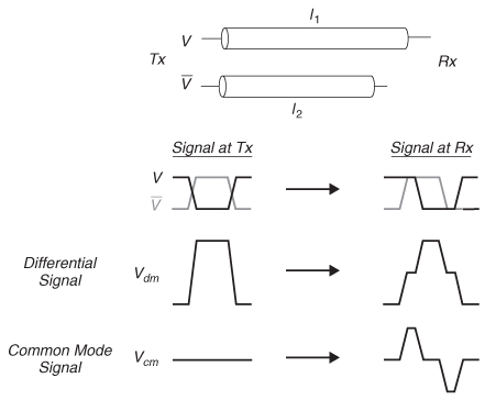
ACCM conversion is caused by asymmetry between V and ![]() in the differential pair. The asymmetry can be caused by length differences, coupling differences, etching differences, proximity effects, termination differences, bends, or anything else that would make one leg of the pair look electrically different from the other. Some of these examples are shown in Figure 7-8. To demonstrate how intrapair asymmetry affects voltage and timing noise, consider the simple (but very common) example where lengths of lines 1 and 2 in the pair are not equal, as shown in Figure 7-8a. Assuming that the signal is launched differentially, the difference in propagation delay between lines 1 and 2 will change the phase relationship at the receiver because the voltage propagating on one leg of the pair will arrive early, converting part (or all) of the differential signal to common mode. Figure 7-9 shows how a perfect differential signal at the transmitter (Tx) is distorted at the receiver (Rx) when asymmetry exists in the pair. The distortion is proportional to the amount of voltage that exists in the common mode.
in the differential pair. The asymmetry can be caused by length differences, coupling differences, etching differences, proximity effects, termination differences, bends, or anything else that would make one leg of the pair look electrically different from the other. Some of these examples are shown in Figure 7-8. To demonstrate how intrapair asymmetry affects voltage and timing noise, consider the simple (but very common) example where lengths of lines 1 and 2 in the pair are not equal, as shown in Figure 7-8a. Assuming that the signal is launched differentially, the difference in propagation delay between lines 1 and 2 will change the phase relationship at the receiver because the voltage propagating on one leg of the pair will arrive early, converting part (or all) of the differential signal to common mode. Figure 7-9 shows how a perfect differential signal at the transmitter (Tx) is distorted at the receiver (Rx) when asymmetry exists in the pair. The distortion is proportional to the amount of voltage that exists in the common mode.
The amount of signal that is converted to common mode depends on the length of the pair, the difference in propagation delays, and the frequency. This
Figure 7-8 Examples of asymmetry in a differential pair that can cause differential to common-mode conversion: (a) routing-length differences; (b) impedance differences due to etching variation; (c) crosstalk differences; (d) length differences due to bends.

Figure 7-9 When asymmetry exists in the differential pair, part of the signal gets converted to common mode at the receiver.
can be shown by calculating the voltage on each leg of the transmission line at the receiver when the signals are launched 180° (π) out of phase:
where β is the propagation constant as defined in equation (6-48c), α the attenuation constant as defined in equation (6-48b), l1 the length of line 1, and l2 the length of line 2. Note that since there is no backward-propagating component (v–), all reflections are perfectly terminated in this example.
The differential-to-common mode conversion (ACCM) is calculated from (7-8a) and (7-8b) with α = 0:
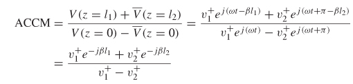
where V(z = l1) and ![]() (z = l2) are the voltages at the receiver, and V(z = 0) and
(z = l2) are the voltages at the receiver, and V(z = 0) and ![]() (z = 0) are the voltages at the driver.
(z = 0) are the voltages at the driver.
At low frequencies where the wavelength is large, the phase delay difference between lines 1 and 2 is small, so the numerator of (7-9) is approximately zero. However, as the frequency increases, the phase difference becomes large. When the phase difference reaches 180° (π), the differential signal launched at the driver is converted completely to a common-mode signal at the receiver, and equation (7-9) is unity.
Example 7-1 For the differential pair shown in Figure 7-10, calculate the frequency where the differential signal injected at the driver is 100% converted to a common-mode signal at the receiver.
SOLUTION
Step 1: Calculate the propagation constant of the transmission lines. Equation (2-46) defines the propagation constant in terms of the wavelength:
![]()
equation (2-45) defines wavelength in the terms of the frequency where the speed of light in a vacuum has been replaced with the speed of light in the media (vp):
and equation (2-52) calculates the speed of light in the media (assuming that μr = 1):

Therefore, the propagation constant is calculated as a function of frequency:

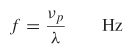
Step 2: Use equation (7-9) to plot the differential-to-common mode conversion. Since V(z = 0) = 1 and V(z = 0) = –1, the terms v1+ = 1 and v2+ = –1. The plot is shown in Figure 7-11. When ACCM = 1, the phase error due to the length mismatch equals 180° and the differential signal launched at the driver shows up as a common-mode signal at the receiver. Therefore, the frequency where the differential-to-common mode conversion is 100% is 12.5 GHz.
Figure 7-10 Figure for Example 7.1.

Figure 7-11 Differential common-mode conversion plotted for Example 7-1 showing that a differential signal launched at the driver becomes common mode at the receiver when the frequency is about 12.5 GHz.
In a differential system, only the difference between V(z = l1) and ![]() (z = l2) is recovered. Consequently, the percentage of differential energy converted to common mode looks like loss to the differential bus in the frequency domain. In Example 7-1 the differential receiver would see no signal at 12.5 GHz. At 4 GHz, approximately 50% of the energy has been converted to the common mode and only one-half the signal would be sensed by the differential receiver.
(z = l2) is recovered. Consequently, the percentage of differential energy converted to common mode looks like loss to the differential bus in the frequency domain. In Example 7-1 the differential receiver would see no signal at 12.5 GHz. At 4 GHz, approximately 50% of the energy has been converted to the common mode and only one-half the signal would be sensed by the differential receiver.
Note that the differential-to-common mode conversion in Example 7-1 decreases after 12.5 GHz. Do not be tempted to operate the bus in this frequency range. The phase difference between signals on the differential pairs will continue to increase until they are 360° out of phase, where (7-9) predicts zero mode conversion. If a digital bus were operated so that the phase difference was 360° at the receiver, bit 1 on line 1 would align with bit 2 on line 2 and the incorrect data would be latched into the receiver. This can easily be demonstrated by observing the real portion of V (z. = l1) and ![]() (z = l2) as calculated with (7-8a) and (7-8b). Figure 7-12a shows the differential-to-common mode conversion (ACCM) for the differential pair in Example 7-1 when l1 = 0.254 m and l2 = 0.340 m. Figure 7-12b shows the real part of V(z =l1 ) and
(z = l2) as calculated with (7-8a) and (7-8b). Figure 7-12a shows the differential-to-common mode conversion (ACCM) for the differential pair in Example 7-1 when l1 = 0.254 m and l2 = 0.340 m. Figure 7-12b shows the real part of V(z =l1 ) and ![]() (z = l2) at the receiver. Note that at low frequencies, the waveforms are 180° out of phase and the differential-to-common mode conversion is zero. At about 880 MHz, the differential-to-common mode conversion is 100%, and the waveforms in Figure 7-12b are in phase. At ~1.75 GHz, the ninth peak of V (z = l1) is 180° out of phase with the seventh peak of
(z = l2) at the receiver. Note that at low frequencies, the waveforms are 180° out of phase and the differential-to-common mode conversion is zero. At about 880 MHz, the differential-to-common mode conversion is 100%, and the waveforms in Figure 7-12b are in phase. At ~1.75 GHz, the ninth peak of V (z = l1) is 180° out of phase with the seventh peak of ![]() (z = l2), and equation (7-9) predicts that ACCM = 0. Although the magnitude of the differential-to-common mode conversion begins to decrease after it peaks, the phase error is large, so the bus will not function properly.
(z = l2), and equation (7-9) predicts that ACCM = 0. Although the magnitude of the differential-to-common mode conversion begins to decrease after it peaks, the phase error is large, so the bus will not function properly.
Figure 7-12 The differential-to-common mode conversion peaks when the difference in phase delay between lines 1 and 2 in a differential pair is 180°. As the phase delay difference increases with frequency, the ACCM becomes zero again, but the phase error is so large that the bus will not operate properly.

7.6.2 Fiber-Weave Effect
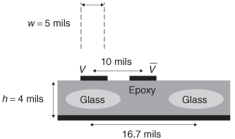
In Section 6.5.1 we described how FR4 and similar dielectrics are composite materials made from a matrix of woven bundles of fiberglass embedded in an epoxy resin. Figure 7-13 depicts how it is possible for one leg of the differential signal to be routed between glass bundles and the other to be routed over a glass bundle that effectively gives each trace a unique propagation velocity. The reinforcing fiberglass bundles have a dielectric permittivity er of approximately 6, whereas er is close to 3 for the epoxy resin in which the bundles are embedded. When a differential pair is aligned with the reinforcing fiber matrix of the dielectric in this manner, it causes an imbalance in the differential pair that causes differential-to-common mode (ACCM) conversion. Even if the lines are routed symmetrically, the difference in the dielectric permittivity will make the electrical delay shorter in one line versus the other. Figure 7-13 depicts a cross section of a differential pair that is asymmetric due to the fiber-weave effect.
Figure 7-13 The fiber-weave matrix used to construct composite dielectrics such as FR4 can cause differential signals to be asymmetric due to the differences in permittivity of the glass weave (εr ~ 6) and the epoxy (εr~ 3). The glass pitch shown is typical for many glass weaves used in the printed circuit board industry.

Unless specific measures are used to eliminate the alignment of the differential pair with the fiber weave, the traditional approach of modeling the transmission line using a uniform dielectric permittivity throughout the dielectric layer is no longer sufficient. The approach must be modified to comprehend the localized dielectric variation. Figure 7-14 shows the profile of the cross-section geometry description used as 2D field solver input for calculating the transmission-line parameters. Simple in principle, this approach is complicated by the fact that the measured effective dielectric permittivity results from the combined effect of multiple dielectrics: resin, fiberglass, solder mask, and air. As a starting point, the effective dielectric permittivity of the FR4 material in each region can be calculated using the measured value of the propagation delay as in Figure 6-15, and the actual dielectric differences can be estimated as described in Section 6.5.1. Alternatively, the results from a 2D field simulation with a cross section that describes the composite nature of the dielectric can be used if sufficient information is available. Many commercial field solvers have this capability, including Ansoft’s Q2D. Nonetheless, once reasonable values for er 1 and er2 are estimated, the fiber-weave effect can be approximated by generating the appropriate transmission-line parameters for each leg of the pair using a cross section similar to that shown in Figure 7-14.
The differential-to-common mode (ACCM) conversion due to dielectric permittivity variations can be calculated using the same procedure that was used to derive equation (7-9). The only difference is that the line length (l) stays constant
Figure 7-14 Cross section for modeling the fiber-weave effect in differential pairs. The dielectric permittivity is adjusted to account for a trace routed over a glass bundle or over an epoxy pool.
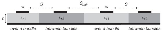
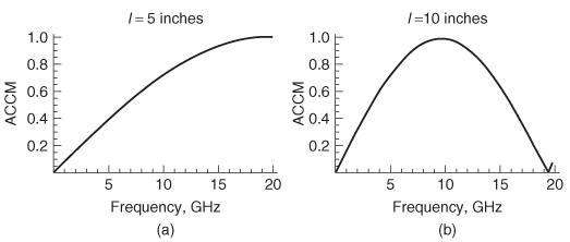
Figure 7-15 Waveforms for Example 7-2: (a) length = 5 in. (b) length = 10 in.
and the propagation constant (β) changes:

where ![]() the differential pair length, and v1+ and v1– are the driving voltages.
the differential pair length, and v1+ and v1– are the driving voltages.
Example 7-2 Determine the frequency where the differential-to-common mode conversion is 100% for a 10-in. (0.254-m) and a 5-in. (0.178-m) differential pair routed where one leg is over a bundle and one leg is between glass bundles. Use the measured data shown in Figure 6-15.
SOLUTION
Step 1: Determine the maximum spread in the effective dielectric permittivity. From Figure 6-15 the spread is 0.23:
![]()
Step 2: Calculate β1 and β2:
Step 3: Plot the differential-to-common mode conversion using (7-10). The plots are shown in Figure 7-15a and b. When the length is 10 in., the differential-to-common mode conversion is 100% at about 10 and 20 GHz for 5 in
Mitigation of the fiber-weave effect was discussed briefly in Section 6.5.2.
REFERENCE
Hall, Stephen, Garrett Hall, and James McCall, 2000, High Speed Digital System Design, Wiley-Interscience, New York.
PROBLEMS
7-1 Assume that a differential pair is routed so that the fiber-weave effect occurs similar to Figure 7-16. Assume that the line is 7 in. long and the metal is copper with a surface roughness of 0.5 µm. If the differential-to-common mode conversion is calculated with losses, how does the answer differ from the case where it is calculated with no losses? Which answer better predicts the percentage of the signal converted to the common mode?
Figure 7-16 The permittivity/loss tangent for the glass weave is εr = 6/tan δ = 0.0002 and the epoxy εr = 3/tan δ = 0.025.
7-2 Derive metrics based on line lengths that will help predict the magnitude of the voltage noise on a digital signal when the fiber-weave effect is present. Use the results of Problem 7-1 for the derivation.
7-3 How would the differential pair of Problem 7-1 affect the timing of a digital signal? (Hint: Consider the phase noise.)
7-4 Describe three different methods for mitigating differential-to-common mode conversion.
7-5 Derive a formula to predict differential-to-common mode conversion for the case where the impedance of each leg does not match.
7-6 Use modal analysis described in Section 4.4 to calculate the differential waveform expected for a 10-in. transmission line with a cross section of Figure 7-16.
7-7 Show that the modal voltages correspond to specific digital states for two signal conductors. Use the following L and C matrices:
7-8 Show that the modal voltages do not correspond to specific digital states for three or more signal conductors. Use the following L and C matrices:

7-9 Use modal analysis to calculate the far-end (forward) crosstalk between two single-ended lines using the matrices in Problem 7-7, and compare it to the crosstalk from a differential pair to a single-ended line using the matrices from Problem 7-8.
7-10 Create a SPICE model that proves how routing guidelines that force signal lines to be routed at 10° or greater angles with respect to the board edge mitigate the fiber-weave effect. (Hint: Review Chapter 6.)