
11
I/O CIRCUITS AND MODELS
11.1 I/O Design Considerations
11.2 Push-Pull Transmitters
11.2.1 Operation
11.2.2 Linear Models
11.2.3 Nonlinear models
11.2.4 Advanced Design Considerations
11.3 CMOS receivers
11.3.1 Operation
11.3.2 Modeling
11.3.3 Advanced design considerations
11.4 ESD Protection Circuits
11.4.1 Operation
11.4.2 Modeling
11.4.3 Advanced design considerations
11.5 On-Chip Termination
11.5.1 Operation
11.5.2 Modeling
11.5.3 Advanced design considerations
11.6 Bergeron Diagrams
11.6.1 Theory and method
11.6.2 Limitations
11.7 Open-Drain Transmitters
11.7.1 Operation
11.7.2 Modeling
11.7.3 Advanced Design Considerations
11.8 Differential Current-Mode Transmitters
11.8.1 Operation
11.8.2 Advanced Design Considerations
11.9 Low-Swing and Differential Receivers
11.9.1 Operation
11.9.2 Modeling
11.9.3 Advanced Design Considerations
11.10 IBIS Models
11.10.1 Model Structure and Development Process
11.10.2 Generating Model Data
11.10.3 Differential I/O Models
11.10.4 Example of an IBIS File
11.11 Summary
References
Problems
So far we have discussed the behavior of high-speed interconnects and have provided techniques for analyzing and modeling the key physical phenomena that affect signal quality at multi-Gb/s data rates. To fully analyze and understand the behavior of high-speed signaling links, we must include the I/O circuits that transmit and receive the digital data. Design of high-performance links demands that the circuits and interconnects be jointly optimized as a unified system. To do so successfully, the signal integrity engineer must be able to communicate with the circuit designer.
In this chapter we describe the operation and modeling of contemporary high-speed I/O circuits, including transmitters, receivers, and on-die terminations. We do not attempt to provide a complete treatment on how to design high-speed I/O; instead, we wish to give the SI engineer insight into the behavior and sensitivities of modern transceivers. This insight is fundamental to developing a sufficient understanding of the interactions between I/O circuits and physical interconnects in order to optimize a signaling system. In this chapter we identify the design parameters of the circuits for use in analyzing and optimizing designs, and describe techniques for modeling I/O circuits. In addition, we introduce the Bergeron diagram, a useful tool analyzing the time-domain behavior of a complete signaling system. Finally, we acknowledge that transceivers can be designed using either bipolar or MOSFET devices, although throughout this chapter we focus on MOSFET-based circuits.
11.1 I/O DESIGN CONSIDERATIONS
The function of a transmitter is to launch a signal representing digital data onto an interconnect for propagation to a receiver circuit. To maximize performance, engineers typically must use design techniques to provide controlled output impedance and rise and fall times. In addition, transmitters (often abbreviated as Tx) can be designed for either singled-ended or differential transmission, and to operate either as a voltage or a current source. In this section we use the term transmitter interchangeably with driver and output buffer, all of which are commonly used in the industry.
A range of complexity for modeling transmitters is possible. At its simplest, the model can be a simple transient voltage in series with an output resistance or a current source in parallel with an output resistance. Since they use simple circuit elements, variation of linear model parameters for the purposes of identifying a working solution and understanding sensitivity to design and process variation is extremely easy. In addition, they are easy to analyze and provide the fastest simulation times. As a result, linear models are very useful for the initial stage of the design process, when large numbers of simulations are performed in order to identify the potential solution space.
More complex nonlinear behavioral transmitter models provide improved accuracy over linear models by comprehending the nonlinear relationship between the output voltage and output current, staged switching of the output devices to control rise and fall times, and parasitic capacitances. Parametric model variation is more difficult than with linear models, but is still possible. Nonlinear behavioral models are widely used (via IBIS, the I/O Buffer Information Spec-ification) because they allow component suppliers to provide accurate models without divulging the specifics of the circuit design and manufacturing process.
Finally, achieving maximum accuracy may require the use of full transistor models. These models are typically used only as a final check of the design, since they are more complex to construct and they require significantly more simulation time. In addition, suppliers are often reluctant to provide transistor models because they can divulge proprietary design and process information. As a result, in this chapter we focus on linear and nonlinear behavioral modeling rather than transistor-level modeling.
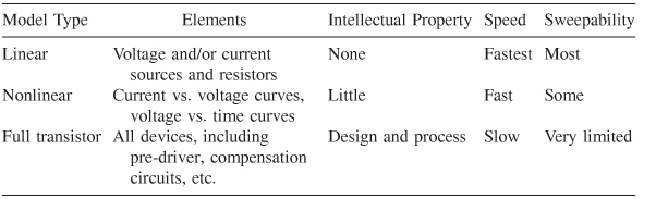
Options for modeling receiver circuits follow the same progression as for transmitters. Simple receiver models include only the termination resistors and input capacitance. Nonlinear behavioral models include the voltage versus current characteristics of the ESD protection circuitry and of terminations that are implemented using transistor devices. Full transistor models incorporate all device effects. Requirements and trade-offs for the various model types are summarized in Table 11-1.
In our modeling discussions in this chapter we focus heavily on linear models due to their extreme usefulness in the early design stages. We also discuss the limitations of such models and give guidance for when to use nonlinear behavioral models.
TABLE 11-1 Summary of Modeling Approaches and Trade-offs
11.2 PUSH-PULL TRANSMITTERS
11.2.1 Operation
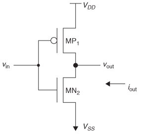
The simplest type of output circuit is a push-pull transmitter, which can be implemented using a simple CMOS inverter (paired with a receiver that is also an inverter in order to preserve the logic state), as shown in Figure 11-1. Push-pull transmitters were popular in the early days of CMOS ICs due to their ease of implementation and low power consumption. They can be used in interconnect systems without termination, with series termination, and/or with parallel termination. A comprehensive description of the operation of CMOS transistors and inverters is provided in a book by Rabaey et al. [2003]. We offer a brief overview here to make sure that the reader understands the fundamentals of push-pull transmitter operation.
We start by providing the expression relating the current conducted by a MOS transistor, io, as a function of the voltage potential applied across the terminal nodes:

Figure 11-1 CMOS inverter transmitter circuit. (From Dabral and Maloney [1998].)
where k = process transconductance (A/V2)
W = device width (μm)
L = gate length (μm)
vGS = potential difference between the transistor gate and source nodes (V)
vT = transistor threshold voltage (V)
vDS = potential difference applied across the source and drain (V)
λ = channel length modulation parameter (V m)
The process transconductance is

where μ is the device mobility (m2/V s), εox the oxide permittivity (F/m), and tox the oxide thickness (m). The oxide permittivity εox is equal to 3.97ε0, and the oxide thickness tox is 5.7 nm for the MOSIS 0.25-μm process. Equation (11-1) describes three distinct regions of operation. In the subthreshold region, where vGS - vT ≤ 0, the device conducts only a very small amount of leakage current. In the triode region, the relationship between the device current and the drain-source potential is approximately linear. In the saturation region, the device enters a high-impedance state, acting like a (nearly) constant current source.
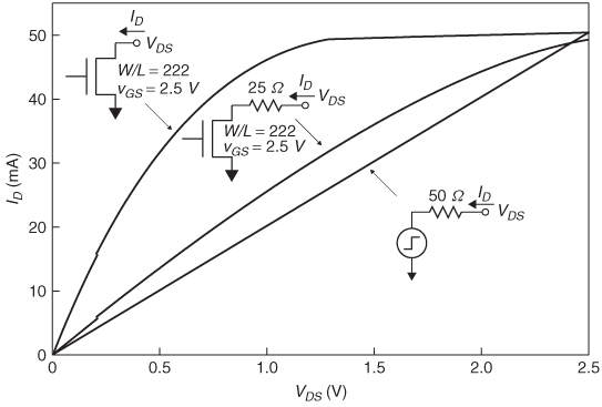
Figure 11-2 shows iD versus vDS curves for various gate-source potentials (vGS) that were created from HSPICE simulation using the SPICE level 3 model for the MOSIS 0.25-μm process that is contained in Appendix F. The dimensions of the devices used to produce the figure are a width W of 222 μm and length L equal to 1 μm for the NMOS transistor and W/L = 845 μm /1 μm for the PMOS transistor. In the case of the PMOS device, VDS is less than zero since vout is less than VDD. As a result, the current flows from the supply (source) to the drain, so that iD is also less than zero. For the NMOS transistor, the polarities for vDS and iD are both positive. Note from the figure that positive current is defined as flowing back into the transistor device. We follow this convention throughout this chapter, although it is equally valid to define positive current flowing in the opposite direction, as long as consistency is maintained.
The voltage transfer characteristic of the inverter shown in Figure 11-3a was created from HSPICE simulation using a SPICE level 3 model for the MOSIS 0.25-μm process with device dimensions identical to those in Figure 11-2. The figure shows how the output signal varies as a function of the input signal level. When the input signal vin is at ground (VSS), the NMOS transistor, MN2, does not conduct current, while the PMOS device, MP1, conducts current according to equation (11-1). As a result, the output signal vout is pulled up to VDD (2.5 V for the 0.25-μm process) through MP1. As the input is raised to VDD, the output drops to ground. At approximately one-half of VDD, the inverter enters a high-gain region in which vout changes rapidly as a function of vin.
Figure 11-2 Example transmitter pull-up and pull-down iD versus VDS curves: (a) NMOS (W = 222 μm, L = 1.0 μm); (b) PMOS (W = 845 μm, L = 1.0 μm).

Figure 11-3b shows the transient response of the inverter when driving a 1-pF load.
11.2.2 Linear Models
The simplest push-pull transmitter model, shown in Figure 11-4, is the linear model. Here the transmitter behavior is modeled by a transient voltage source in series with a resistor (i.e., a Thevenin equivalent circuit). The voltage source
Figure 11-3 Example CMOS transmitter input-output characteristics: (a) voltage transfer characteristic; (b) transient response driving a 1-pF load.

Figure 11-4 Linear (Thevenin) equivalent model for a CMOS transmitter (a) basic model; (b) with output capacitance, CS .

Figure 11-5 Example transient response for a linear transmitter model.

Limitations of the linear model The nonlinear relationship between output current and node voltages for real MOS transistors creates the potential for significant behavioral differences between the linear model and a real transmitter, which we illustrate by example.
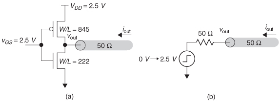
Example 11-1 Load-Line Analysis Using a Linear Transmitter Model We compare the falling-edge behavior of interconnect circuit shown in Figure 11-6a with that of the linear model in Figure 11-6b. The current versus voltage characteristic for the pull-down transistor is described in Figure 11-2a for vGS = 2.5 V. To calculate the actual impedance of the transmitter, we use a technique known as a load-line plot [Rabaey et al., 2003] We start with a plot of output current versus output voltage for the NMOS transistor. Recognizing that the falling-edge transition for this circuit begins from a state in which no current flows (i = 0) and the voltage is 2.5 V, we construct a load line for the transmission line that expresses the output current as a function of the output voltage using Ohm’s law:
![]()
The current versus voltage plots for both the transistor and transmission line are shown in Figure 11-7. The intersection of the two lines gives the values for the voltage and current at the transmitter output when driving the transmssion line for the falling edge (0.650 V, 37 mA). The NMOS transistor was sized to conduct 50 mA across a potential of 2.5 V, which would provide an output impedance RS of 50Ω. However, as the figure demonstrates, the transmitter actually conducts more than 95% of the maximum current by the time the output swing has reached one-half of the maximum value (1.25 V). As a result, the transmitter has an effective output impedance of approximately 0.65 V/37 mA = 18Ω as seen by the transmission line.
Figure 11-6 Interconnect circuit for Example 11-1: (a) circuit with push-pull transmitter; (b) linear model.
For the linear model, we construct the voltage-current plot using Ohm’s law.
![]()
Figure 11-7 Load-line plot for Example 11-1.
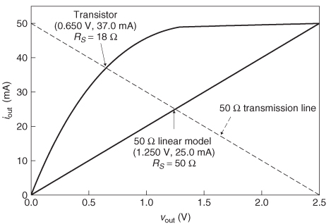
The linear model provides an initial output voltage and current of 1.250 V and 25 mA when driving the 50-Ω transmission line. Thus, the linear model is a clear source of inaccuracy for modeling an interconnect system, although it may be good enough for low-speed designs or for use in the early design stages of a high-speed link.
We have two options at our disposal if a better match between design and model is required. The first is to modify the transmitter design to give it a more linear current-voltage relationship. This is most easily accomplished by placing a resistive element in series with the output transistor. From Example 11-1 we note that the transmitter actually conducts more than 95% of the maximum current by the time the output swing has reached one-half of the maximum value (1.25 V). As a result, the transmitter has an effective output impedance of approximately 25 Ω across the output voltage range 0 to 1.25 V (the linear region of operation) and a very high impedance from 1.25 to 2.5 V (the saturation region). By adding a 25-Ω resistor in series with the effective 25 Ω of the transistor, we can better approximate the desired 50-Ω impedance, as shown in Figure 11-8.
Since it requires modifying the design, this approach is typically taken only when a constant impedance over the entire voltage swing is critical to the design [Esch and Chen, 2004]. An example is the AGP4X interface, which used a series-terminated interconnect to transmit graphics data at 266 Mb/s. The interface relied on the transmitter to provide the termination, which required linearization of the voltage-current relationship [Intel, 2002].
Figure 11-8 Comparison of push-pull transmitter current versus voltage characteristics to a linear model.
11.2.3 Nonlinear models
The other option for improving accuracy is to use a nonlinear model. In addition to the nonlinear current-voltage characteristic, this type of model can also comprehend the shape of the rising and falling edges of the output. The basic push-pull nonlinear model consists of an output current versus output voltage curve for both pull-up and pull-down devices and an output voltage versus time curve for both the rising and falling edges (Figure 11-9). In addition to the curves, a nonlinear behavioral model typically contains the load conditions under which the curves were constructed. Simulation tools use this information, typically in the form of an IBIS model (see Section 11.10), to adjust the model for the differing load conditions encountered when it is used in simulations of real interconnect systems.
Figure 11-9 Nonlinear behavioral model components: (a) pull-up iout versus vout; (b) pull-down i out versus vout; (c) rising edge vout versus time; (d) falling edge vout versus time.

The device capacitance may also be included, if it is not already comprehended in the transient voltage versus time curves of the model. However, models created from either transistor-based simulations or from measurements typically include the effects of the capacitance, in which case it should not be explicitly called out in the model. Construction of the iout versus vout curves is discussed further in Section 11.10.
In general, simulation tools create multiple i - v curves to account properly for the transient nature of the input signal to the model. Stated another way, a time-varying input signal, vin, to the circuit in Figure 11-1 causes the device gate-to-source potential, vgs, to also be transient, so that the output current-voltage relationship varies with time as well. This effect is shown in Figure 11-10 and Table 11-2 for an inverting transmitter. The rising-edge input signal starts at a value of 0.0 V, which corresponds to vgs = 0.0 V for the NMOS device and to vgs = -2.5 V for the PMOS device. As the input edge rises, the vgs values for each device change. For example, when Vin is equal to 1.0 V, vgs is 1.0 V for the NMOS device and -1.5 V for the PMOS device. We see that for the case of a rising-edge input signal, as the PMOS device moves from the vgs = -2.5 V curve to the vgs = 0 V curve, the NMOS device is transitioning from the curve for vgs = 0 V to that for vgs = 2.5 V.
As a final note, we point out that the i - v data in the model should extend well beyond the expected operating range for the device to ensure proper operation in the event of significant signal overshoot. For example, if the signal swing expected ranges from 0 to VDD, the IBIS specification expects that the i -v data span a range from - VDD to 2VDD.
11.2.4 Advanced Design Considerations
In this section and in the counterpart sections for other transceiver types, we touch briefly on several of the issues that face circuit designers when developing transmitter circuits. For more extensive discussions of the issues and techniques, we refer the reader to books by Dabral and Maloney [1998] and Dally and Poulton [1998].
Overlap current control When the transmitter circuit of Figure 11-1 makes a rising or falling transition, the PMOS and NMOS devices will conduct current simultaneously for a brief period of time. The magnitude of this overlap current (also known as “crowbar” current) is sufficiently high that designers usually design the transmitter such that the initially conducting device turns off before the other device turns on. This is typically implemented with “pre-driver” control logic.
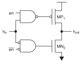
Tristate function Systems in which multiple devices can drive a common signal, such as a multiprocessor bus, require that the transmitter be placed in a high-impedance state when it is not actively driving the system. This is also accomplished with pre-driver logic, as shown in Figure 11-11. The circuit uses the enable signals, en/![]() , to control whether the transmitter is connected and can actively drive the bus, or is disconnected and presents a high impedance, as described by Table 11-3.
, to control whether the transmitter is connected and can actively drive the bus, or is disconnected and presents a high impedance, as described by Table 11-3.
Process and environmental compensation When fabricating large numbers of components, the physical features (e.g., gate length, oxide thickness) and electrical characteristics will vary due to normal statistical variations in the manufacturing process. In addition, MOSFET currents are sensitive to environmental factors such as supply voltage (iD increases as the VDD increases) and device temperature (iD decreases with increasing T). As a result, the current-voltage relationship for transistors can vary by a factor of 2 to 3 across the process and environmental extremes, leading to wide swings in the output impedance and rise-fall time. In the case of microprocessor-based systems, where yearly volumes reach into the hundreds of millions, excessive variation in the electrical characteristics can lead to failure of some of the systems to operate at full performance. Compensation refers to techniques that minimize the variation between different parts operating in different environments. Designers can implement compensation using both digital and analog techniques, which are used most often to provide carefully controlled impedance and/or rise and fall times. Although a detailed discussion of those techniques is beyond our scope, we present an example of digital impedance compensation to illustrate application of the concept.
Figure 11-10 Interaction between vin-t and i out- vout curves for an inverting push-pull driver: (a) transient input signal; (b) i - v curve progression for the PMOS pull-up; (c) i - v curve progression for the NMOS pull-down.

TABLE 11-2 Relation Between vin and vGS for the Pull-up and Pull-down Devices of an Inverting Transmitter
| vGS (V) | ||
| vin (V) | NMOS | PMOS |
| 0.0 | 0.0 | -2.5 |
| 0.5 | 0.5 | -2.0 |
| 1.0 | 1.0 | -1.5 |
| 1.5 | 1.5 | -1.0 |
| 2.0 | 2.0 | -0.5 |
| 2.5 | 2.5 | 0.0 |
TABLE 11-3 Logic Table for a Tristate Transmitter
| en/ | vin | vout |
| 0/VDD | X | High Z |
| VDD/0 | VDD | 0 |
| VDD/0 | 0 | VDD |
Figure 11-11 Tristate push-pull driver.
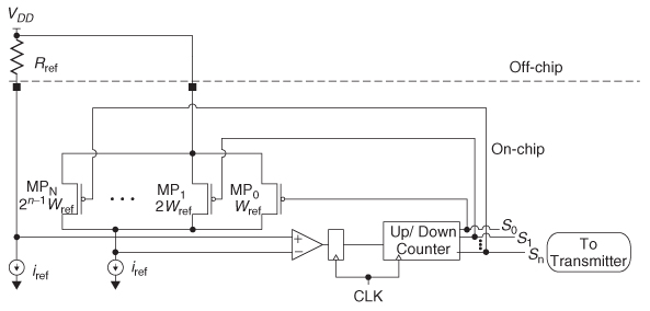
Example 11-2 Digital Impedance Compensation The circuit shown in Figure 11-12 will provide controlled impedance for either the output of a transmitter or for on-die termination resistors (see Section 11.5). The circuit adjusts the impedance to closely match a desired value by comparing the strength of a binary weighted on-die replica circuit (PMOS transistors MPo through MPN) with that of an external precision resistor (typically controlled to ±1%). Both are connected to identical reference current sources (iref), forming voltage dividers whose levels are fed into the clocked comparator at the bottom of the figure. The output from the comparator is used to increment/decrement an up/down counter. The output signals (So to S2) from the counter control the turn on-turn off of devices MPo to MPN, which decreases or increases the impedance of the control network to achieve the desired impedance. Signals S0 to SN are also connected to the transmitter circuits, each of which contains a similar structure, thus providing the controlled impedance characteristic.
Since it operates from a clock, the circuit can adjust the impedance dynamically to compensate for variation in the supply voltage and device temperature during operation. In this case the clock is a low-frequency clock that is updated about every millisecond. In addition, the design should also ensure that the control bits do not change while the circuit is actively driving in order to avoid noise on the signals due to changing impedance [Gabara and Nauer, 1992]. Achieving tighter impedance control is simply a matter of adding additional binary weighted devices.
Figure 11-12 Digital impedance compensation circuit.
11.3 CMOS RECEIVERS
The most basic receiver for interchip signaling circuits is the inverter. The simplicity, low power consumption, and ease of implementation of inverters made them the receiver of choice for full-swing CMOS-based interfaces through much of the 1990s. Receivers are characterized by timing parameters (setup and hold) and by logic thresholds, which influence system noise margin and noise immunity. Our discussion of the operation of merits of receivers for high-speed signal transmission will focus on these characteristics.
11.3.1 Operation
The CMOS receiver is a low-gain inverting amplifier that provides full rail-to-rail output swings, which allows for fairly large noise margins at speeds into the hundreds of Mb/s. Figure 11-13a illustrates the voltage transfer characteristic for an example inverting receiver, which specifies the output signal as a function of the input. The input thresholds vil and vih are determined by the unity gain points (dvout/dvin = - 1) of the transfer characteristic. The region in between vil and vih is a high-gain region in which the output signal level is extremely sensitive to variations in the input signal, making it a forbidden “keep out” area for steady-state signals.
Large noise margins provide tolerance to noise sources, and so are desirable to guarantee robust operation. As Figure 11-13b demonstrates, the high-side noise margin, vNMh, is the difference between the minimum output signal when driving high and the minimum signal that the receiver recognizes as the high logic state. Conversely, the low-side noise margin, VNMl, is the difference between the maximum output signal when driving low and the maximum signal recognized by the receiver as the logic low state. Note from the figure that the receiver input specs must comprehend variations in the signal levels caused by variability in the fabrication process. Mathematically, the noise margins are expressed as
Figure 11-13 CMOS receiver response characteristics: (a) voltage transfer characteristics; (b) noise margin.

11.3.2 Modeling
The CMOS inverter presents a high impedance to the input signal, limited only by the input capacitance of the gate. As such, we typically model a CMOS receiver as a simple capacitance to ground.
11.3.3 Advanced design considerations
Though the relatively large swing results in high noise margins, voltage mode signaling systems possess multiple noise sources that degrade the noise immunity of the system [Dally and Poulton, 1998]. For example, process variations such as device thresholds and transconductance can cause inverter thresholds to vary by more than 10% of the signal swing (>20% if supply voltage variation is included), a phenomenon known as receiver offset. Other sources include power supply noise, crosstalk, reflections, and transmitter offset.
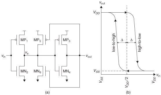
These effects may be countered by designing additional noise tolerance into the receiver through hysteresis. An example is a Schmitt trigger, which we show in Figure 11-14a [Wang, 1989]. The MPI/MN2 and MP3/MN4 transistors form a sequential pair of inverters. The hysteresis is created by feeding the output vout back to the gates of MP5 and MN6, which shifts the voltage transfer characteristic, making it more difficult for a noise pulse to put the circuit into the keep-out Zone, as Figure 11-14b shows.
11.4 ESD PROTECTION CIRCUITS
Transceiver designs include electrostatic discharge (ESD) protection circuits to prevent catastrophic failure due to breakdown of the MOSFET gates of the I/O and core circuits. ESD damage can occur at any point during the manufacture, assembly, test, and operation of a silicon chip, including handling and transport. An example would be a technician wearing rubber-soled shoes on a test floor. The insulating characteristics of the rubber can cause the technician to accumulate a substantial static charge, which may discharge into any component with which he or she may come into contact, damaging the component. An example ESD event based on a human body model can have a 3000 to 5000-V potential spike with a sub-10-ns rise time, 1 to 2-A peak current, and 100 to 200-ns duration [Dabral and Maloney, 1998]. The device oxide will break down at field strengths in excess of about 7 x 10⁸ V/m, which translates to voltages in excess of approximately 4.0 V for a 25-μm silicon process. So an ESD event can exceed the process limits by several orders of magnitude, necessitating the inclusion of ESD protection in the I/O circuitry.
Figure 11-14 CMOS receiver with hysteresis: (a) Schmitt trigger receiver circuit; (b) voltage transfer characteristic.
11.4.1 Operation
ESD protection circuits such as the one shown in Figure 11-15 protect active circuits by limiting the voltage excursions so that they do not exceed the breakdown voltage of the receiver MOSFET gates, and by limiting the amount of current that flows into the transmitter device terminals. The function of the ESD diodes is to limit the voltage so that it does not exceed the gate oxide breakdown voltage and to steer the ESD current away from the internal circuits. If the voltage at the pad will be greater than a diode voltage drop (VD,on) beyond the VDD supply, the upper diode will turn on, shunting the current away from the I/O device and clamping it to VDD + VD, on. A negative excursion will be clamped to a value of VSS - VD, on The series resistor limits the amount of current that flows through the transceiver devices to prevent performance degradation due to device threshold shifts caused by “hot” electron tunneling [Dally and Poulton, 1998].
11.4.2 Modeling
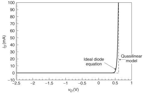
The diodes add parasitic capacitance to the transceiver, which we include in our linear model. The series resistance is typically several hundred ohms, and does not require explicit modeling. Nonlinear models must take into account the current-voltage relationship of the diode, which is given by the ideal diode equation:
Figure 11-15 CMOS receiver with ESD protection.

where idiode is the current through the diode; is, the diode saturation current, is proportional to the diode area; vdiode is the bias voltage across the diode; and is ϕT the thermal voltage (26 mV at room temperature).
Figure 11-16 presents an example current-voltage characteristic calculated using equation (11-4) ϕT with equal to 26 mV and a saturation current of 10 pA. We can further approximate the diode behavior for manual analysis by setting the diode current to zero below the “turn-on” voltage (approximately 0.6 V in the figure) and allowing it to approach infinity at the turn-on voltage. This is shown as the quasilinear model in the figure. We illustrate the use of the quasilinear model in Problem 11.6.
Figure 11-16 Example diode current-voltage characteristic and quasilinear approximation.
11.4.3 Advanced design considerations
The circuit shown in Figure 11-15 is but a simple example of ESD protection. In reality, designers have many options for implementing ESD protection, and often go to great lengths to design structures that provide sufficient protection while minimizing the parasitic capacitance for high-speed operation. We refer the reader to the books by Dally and Poulton [1998] and Dabral and Maloney [1998] for comprehensive treatment of the topic.
11.5 ON-CHIP TERMINATION
On-chip (a.k.a. on-die) termination has become the method of choice as signaling speeds continue to increase, since it eliminates a source of reflections by removing the transmission-line stub that is required to connect off-die termination.
11.5.1 Operation
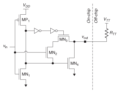
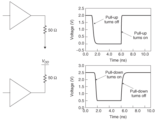
Termination resistors are typically implemented using FETs. An example is shown in Figure 11-17, in which PMOS and NMOS devices are connected in parallel to create a 50-Ω termination to VDD (2.5 V for the 0.25-μm process). The PMOS gate is connected to ground (vgs = -2.5 V) and NMOS to VDD (vgs = 2.5 V) to keep the transistors in the triode region for as long as possible in order to make the current-voltage relationship as linear as possible. As the figure shows, this configuration provides a termination of approximately 46 to 58 Ω over the entire range of operation for nominal device characteristics and operating conditions. Figure 11-17b shows the waveforms obtained when using the circuit to terminate a 50-Ω transmission line when driven with a 2.5-V 12.5-Ω linear transmitter. The FET termination provides nearly equivalent performance to a perfect 50-Ω resistive termination. We also note that our choice to terminate to the positive supply rail rather than ground was also based on making the termination as linear as possible. FET termination is typically combined with the digital impedance compensation technique described in Section 11.2.4 to provide a controlled impedance termination across process, voltage, and operating temperature.
11.5.2 Modeling
The basic model for on-chip termination is a simple resistor connected to the appropriate termination supply. However, as we showed earlier, on-chip termination can exhibit significantly nonlinear response, in which case we need to model the termination as a table of current and voltage values using a nonlinear modeling format such as IBIS (refer to Section 11.10).
Figure 11-17 Example on-chip termination using parallel FETs: (a) FET termination circuit and resistance as a function of line voltage; (b) example waveform.

11.5.3 Advanced design considerations
The primary motivation for implementing on-chip termination is to minimize reflections by eliminating the transmission line stub that is typically required when terminating on the printed circuit board. To fully realize the potential benefit of on-chip termination, automatic impedance control similar to the impedance-matching technique described in Section 11.2.4 is commonly used. In addition, designers may implement techniques to improve the linearity of the on-chip termination [Dally and Poulton, 1997].
11.6 BERGERON DIAGRAMS
At this point we take a slight detour from our survey of transceivers to introduce the Bergeron diagram, a technique that will allow us to analyze the behavior of interconnects with nonlinear transmitter and receiver characteristics by graphically solving the simultaneous current-voltage relationships of the components of a signaling system. We introduce this technique as it is useful for furthering our understanding of transmission-line basics. We demonstrate and develop the technique through a simple example.
Example 11-3 Bergeron Diagram for a Linear Interconnect Circuit In this example we analyze the rising behavior for the circuit shown in Figure 11-18. The transmitter is a 2.5-V push-pull driver with symmetrical pull-up and pull-down impedances. The receiver has a resistive termination to a 2.5-V termination supply.
We start the analysis by plotting the current versus voltage relationships for the transmitter and receiver. The easiest way to do so is to draw the equivalent circuits and write the Ohm’s law expressions. This is shown in Figure 11-19 along with the load-line plot. Note that we were careful to account correctly for the direction of the current flow in all of the equivalent circuits and that we chose to use milliamperes as the units for the y-axis. Note from the plot that the intersection of the transmitter pull-down and the receiver load lines gives the voltage and current (0.357 V and 28.6 mA) for the circuit at the steady state when driven low. Since the circuit is at steady state, this is the potential and current flow at all points on the transmission line. This gives us the starting point for our analysis, since we are studying a rising-edge transition.
Our next step is to find the initial voltage and current for the rising edge at the transmitter. We do this by drawing a load line representing the 50-Ω transmission line, starting at the intersection of the transmitter pull-down and receiver (steady-state low) and extending until it intersects with the load line for the transmitter pull-up. This load line has a slope equal to - 1/Z0, since the transmission line also obeys Ohm’s law and the load line is a plot of current versus voltage. In effect, the load line for the transmission line is graphically depicting the Ohms’ law equation:
Figure 11-18 Interconnect circuit for Example 11-3.

where v0 and i0 are the steady-state voltage and current for the system when driven low. The slope of the line is negative because the rising-edge transition causes current to flow from the transmitter into the transmission line, while we have defined positive current as flowing from the line back into the transmitter.
The transmitter also follows Ohm’s law, so that the intersection between the transmission line and the transmitter pull-up lines gives the initial voltage and current at the transmitter for the rising edge. Figure 11-20a illustrates this, giving an initial voltage and current of 2.357 V and -11.4 mA.
Figure 11-19 Equivalent circuits and voltage-current expressions for Example 11-3: (a) transmitter pull-up; (b) transmitter pull-down; (c) receiver; (d) load-line plot.

The next step is to draw another load line for the transmission line. The line starts at the previous point (2.357 V, -11.4 mA), has a slope equal to 1/Z0, and extends until it intersects with the load line for the receiver, as shown in Figure 11-20b. This gives us the voltage and current at the receiver after the first propagation delay, and comprehends both the initial and reflected waves. It works because we are again satisfying simultaneous Ohm’s law expressions for the transmission line and the receiver, while taking into account the previous voltage and current levels. Ohm’s law gives us the relationships that allow us to solve for the signal values given the constraints imposed by Kirchhoff’s circuit laws. Since the transmission line is connected to the receiver, Kirchhoff’s circuitμmlaws tell us that they will have equal voltages at the connection and equal currents flowing through them. Thus, our Bergeron diagram gives us the solution to two simultaneous Ohm’s law equations in two unknowns (the voltage and current) via graphical means.
By continuing to draw load lines for the transmission lines with slopes that alternate between ±1/Z0 we can find the voltage and current levels at each end of the line as the waves propagate back and forth. For example, Figure 11-20c shows the extension of the next transmission load line back to the transmitter load line, which gives the signal levels at the transmitter after a round-trip propagation delay. The transient wave components are becoming small enough at this point that they are difficult to discern, so Figure 11-20d shows a close-up view of the diagram.
Figure 11-20 Bergeron diagram construction sequence for Example 11-3: (a) initial wave at transmitter (t = 0); (b) receiver (t = td); (c) transmitter (t = 2td); (d) close-up: transmitter (t = 2td).
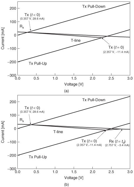
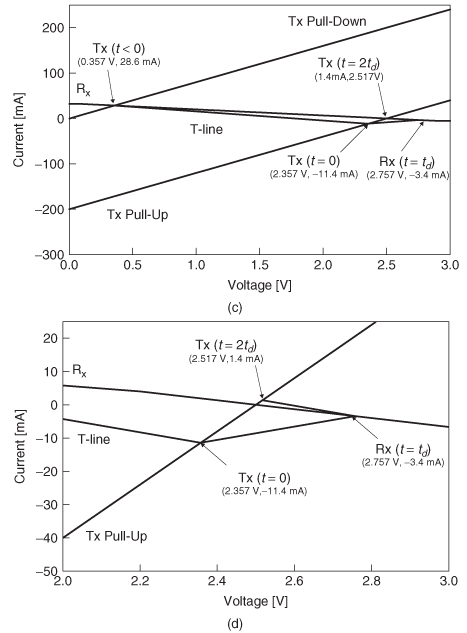
The process of drawing load lines continues until the changes in voltage and current become small enough to suit our need. We can then construct voltage and current waveforms by reading the values from the Bergeron diagram. We must keep in mind that points that occur at intersections with the transmitter load line contribute to the transmitter waveform, and points that occur at intersections with receiver load line contribute to the waveform at the receiver. The full Bergeron diagram is shown in Figure 11-21 along with the voltage and current waveforms.
At this point we note that we generated the voltage and current numbers shown in the waveforms by repetitively solving simultaneous Ohm’s law equations subject to initial voltages and currents-the analytical equivalent of the Bergeron diagram. In practice, drawing a Bergeron diagram with better than 5mV, 0.5 mA accuracy is difficult, which limits its use primarily to initial, first-order estimates.
Figure 11-21 Complete Bergeron diagram and resulting waveforms for Example 11-3: (a) Bergeron diagram; (b) voltage waveform; (c) current waveform.

11.6.1 Theory and method
The Bergeron diagram works by using Kirchhoff’s circuit laws at the connections between the transmission line and the transmitter and receiver components, along with the current versus voltage relationships. For the transmission line, the current and voltage are related by Ohm’s law. The linear transmitter and receiver models that we used in our previous example also obey Ohm’s law, although nonlinear models will obey the more complex relationships described by equations (11-1) and (11-4). The Bergeron diagram also works with nonlinear transceivers, as we show in the next section.
In describing the theory behind the Bergeron diagram, we use the generalized circuit shown in Figure 11-22 with a rising signal. We start at the steady state prior to the rising transition. Under steady-state conditions a lossless transmission line is a short circuit, so that the output of the transmitter is connected effectively directly to the receiver. In our discussion here, when we refer to the transmitter and receiver we mean the equivalent circuits for each, as shown in Figure 11-22. At steady state, we know that the current flowing out of the equivalent circuit for the transmitter is equal to the current flowing into the equivalent circuit for the receiver from Kirchhoff’s current law. From Kirchhoff’s voltage law we know that the voltage at the output of the transmitter equivalent circuit is equal to the voltage at the input of the receiver equivalent circuit. We also know that the relationship between the current and voltage at the output of the transmitter follows Ohm’s law, as does the current-voltage relationship at the input of the receiver. By equating the voltages and currents and applying Ohm’s law, we create a set of two simultaneous equations in two variables:
Figure 11-22 General linear circuit for Bergeron analysis.
The Bergeron diagram solves the equations graphically to give the steady-state current and voltage.
To find the voltage and current values for the initial transition at the transmitter end of the circuit, we recognize that the output of the transmitter is connected to one end of the transmission line. By applying the circuit laws in the same manner as above, we calculate the initial voltage and current wave magnitudes at the transmitter. However, the Ohm’s law expression for the transmission line must comprehend the initial current and voltage flowing through the line:
Note from equation (11-9) that the slope of the load line for the transmission line is equal to - 1/Z0, just as we constructed it in our example. So the Bergeron diagram again solves the simultaneous equations while accounting for the steady-state potential and current flow that existed on the line prior to the transition.
When the initial wave reaches the connection between transmission line and receiver, we again apply the circuit laws and account for the current and voltage of the incident wave:
The slope of this load line for the transmission line is 1/Z0 because it relates the current and voltage for the reflected wave, and since we must account for the current and voltage of the incident wave, it starts at the current and voltage, i(t = 0) and v(t = 0), that we calculated in the preceding step.
The next step in the analysis returns back to the transmitter end of the system using a load line with slope - 1/Z0 starting from the receiver voltage and current (i.e., the intersection between the previous transmission line load line and that of the receiver). In this case the load-line slope is negative because we are accounting for the reflected voltage and current waves at the transmitter. Since the waves flow away from the transmitter and toward the receiver, the sign of the current wave is negative.
The analysis continues in this fashion, alternating between transmitting and receiving load lines using transmission load lines with alternating slopes of- 1/Z0 and 1/Z0, until it approaches steady state. So we see that the Bergeron is simply a graphical technique for repeatedly solving the simultaneous equations arising from circuit laws that describe the transient voltage and current signals at both ends of a transmission line. We now illustrate the application of the technique to a system with nonlinear transceiver characteristics.
Example 11-4 Bergeron Diagram with Nonlinear Transceivers In this example we analyze the falling edge for the circuit shown in Figure 11-23, which uses a CMOS push-pull transmitter with no termination at the receiver end. The system relies on the output impedance of the transmitter to provide source termination, and the transistors are sized to provide a 50-Ω output impedance to match the target impedance of the transmission line. The load-line plot shows the nonlinear transistor behavior discussed in Section 11.2.1. The load line for the receiver is simply a zero-current (infinite-impedance) line that represents the open circuit at that end. We know that the characteristic impedance of the transmission lines may vary by up to ±20% due to manufacturing tolerances. Thus, for our example we choose a 60-Ω characteristic impedance for the transmission line. With this information, we step through the analysis as follows:
1 The Bergeron diagram begins at the load-line intersection of the transmitter pull-up and the receiver. The potential and current are 2.5 V and 0 mA, respectively.
2 From that point we draw the load line for a transmission line with slope equal to -0.0167 Ω-1 (-1 /60 Ω), extending it until it intersects the nonlinear curve for the transmitter pull-down device at 0.80 V and 28.3 mA, which are the initial values at the transmitter after the falling-edge transition.
3 Draw a load line from the previous point, with slope equal to 0.0167 Ω-1 until it intersects with the receiver load line at i = 0, which gives the voltage at the receiver (-0.90 V) after the first incident wave reaches it. A simple means of checking the result at this point is to consider the magnitudes of the incident and reflected voltage waves. The incident-wave magnitude is equal to 0.80 V -2.50 V, or -1.70 V. The reflected wave is also equal to -1.70 V (-0.90 V -0.80 V). Since the transmission line is open-circuited at the receiver end, this is exactly the result that we expect to find.
Figure 11-23 Push-pull transmitter circuit and nonlinear i -v characteristics.
4 Draw the next load line, starting at -0.900 V and 0 mA with slope equal to -0.0167 Ω-1 until it intersects the transmitter pull-down curve, which yields the voltage (-0.25) and current (-10.8) at the transmitter after the first reflected wave from the receiver reaches it.
5 Continue the analysis until reaching steady state (0.00 V, 0 mA).
The resulting voltage waveforms at both ends of the line are shown in Figure 11-24b.
Figure 11-24 (a) Bergeron diagram and (b) transient waveforms for Example 11-4.
11.6.2 Limitations
As mentioned earlier, the accuracy of Bergeron diagrams is typically around 5 mV and 0.5 mA, limiting their use to the earliest stage of the design process. In addition, they can only handle impedance discontinuities at the ends of the lines, so they are not suitable for analysis of more realistic (and complex) topologies. Finally, they only work for lossless transmission lines, which limits their application to data rates in which losses may be ignored. Despite these limitations, Bergeron diagrams provide a means of evaluating the impact of I/O circuit nonlinearity, making them a helpful tool in the arsenal of the signal integrity engineer.
11.7 OPEN-DRAIN TRANSMITTERS
A second type of transmitter circuit is the open-drain transmitter, which is shown in Figure 11-25. An example is Gunning transceiver logic (GTL) [Gunning et al., 1992] As the figure shows, open-drain systems are typically designed using only NMOS pull-down transistors, so that the PMOS pull-up device is eliminated. Ensuring proper function requires the addition of pull-up resistors. The resistors may be added as external components, but state-of-the-art designs typically include them on the silicon die. Note the presence of a termination supply, VTT , which is typically a low voltage in the range 1.2 to 1.5 V, as open-drain systems are usually implemented with signal swings in the range 800 to 1000 mV.
11.7.1 Operation
When the open-drain transistor is turned off, the transmitter is effectively disconnected from the interconnect, which is pulled up to the termination supply through the termination resistor, RTT . No current flows when the interconnect is in the high state, since it is open circuited. When the open-drain transistor is turned on, it effectively creates a voltage-divider circuit by creating a path for current flow from the VTT supply through the termination resistor and the NMOS transistor. As a result, open-drain systems do not use “rail-to-rail” signal swings, since the signal level does not reach ground when driving low.
Figure 11-25 Open-drain signaling circuit.
Benefits Open-drain designs offer multiple potential benefits that have made them a popular design choice over the past two decades. The use of parallel termination reduces reflections for higher-speed applications, and elimination of the PMOS pull-up output transistors reduces the amount of die area consumed, which creates the potential to reduce the cost of the silicon. Since open-drain designs do not dissipate power in the high state, they are typically defined as being active low, in order to achieve zero power consumption when idle. In addition, in contrast to push-pull circuits, the small signal swing reduces active switching power. These features combine to make open drain a popular choice for low-power designs.
Another benefit of open-drain systems is their ability to interface components that are manufactured on different processes that have differing maximum voltage supply limits. Use of the low-voltage external termination supply allows us to decouple the signaling values from the component supplies. For example, GTL uses a 1.2-V external supply, and signals swing from 0.4 V to 1.2 V. This would allow us to connect a component that uses a 3.3-V supply rail with one that uses a 2.5-V rail.
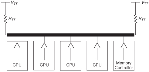
Finally, open-drain systems provide a “wired-OR” function for multiprocessor systems, in which any one of multiple agents can assert an active signal on the bus interface (see Figure 11-26). An example is the MCERR# (machine check error) signal on the Intel Xeon processor system bus interface (a.k.a. front-side bus). MCERR# is asserted (driven low) to indicate an unrecoverable error. Since multiple agents may drive this signal at the same time, it is a wired-OR signal that must connect the corresponding pins of all processor front-side bus agents [Intel, 2005]. Wired-OR connections are susceptible to “glitches” that can occur when multiple agents drive the bus low simultaneously. In Problem 11-10 we explore this phenomenon in more detail.
Figure 11-26 Multiprocessor system with open-drain wired-OR connection.
Limitations Despite the use of parallel termination, GTL is susceptible to ringing on rising-edge transitions. The reason for this is that when the device turns off, the transmission line is open circuited at the transmitting end. Any reflections on the interconnect that travel back to the transmitter will undergo a full reflection, as we show with an example.
Example 11-5 Rising-Edge Reflections in an Open-Drain Interconnect The interconnect circuit in Figure 11-27 has an impedance discontinuity between boards 1 and 2. To analyze the behavior of the rising edge, we follow the current-mode analysis method [Hall et al., 2000]. We model the open-drain device as an effective resistance, RS, with a switch. The analysis starts with the circuit at steady state when driven low. Prior to t = 1 ns, the switch is closed, and a steady-state current flows:
The switch opens at t = 1 ns, creating an open circuit at z = 0. The open circuit requires that the net current flow is zero at that point. The consequence of this is that a -16-mA current wave is launched onto the 75-Ω line, creating a 1.2-V voltage wave. From that point we can carry out the analysis using a lattice diagram, which we shown in Figure 11-27b. Figure 11-27c shows the resulting waveform at the transmitter and at the receiver, which demonstrates the ringing at both ends of the system, despite the fact that the termination matches the impedance of the second line.
11.7.2 Modeling
A linear model for an open-drain circuit requires a resistor and a switch, as shown in Figure 11-28. In addition, a termination supply and termination resistor are required to complete the open-drain system. The means for modeling the switch will vary between different simulation tools. In HSPICE, the easiest method is to use a voltage-controlled resistor [Synopsis, 2006]. Nonlinear models for open-drain transmitters look similar to those for push-pull transmitters, except that the current-voltage relationship for the pull-up is a straight line at i = 0.
11.7.3 Advanced Design Considerations
As discussed above, the finite output impedance of an open-drain transmitter provides some damping of reflections when driving low. However, the transmitter will fully reflect any incoming signals on the rising edge as the open-drain device enters the high-impedance state. A straightforward way to address the ringing caused by the impedance mismatch is to add a termination resistor to provide impedance matching at the transmit end of the system, as shown in Figure 11-29. Although this technique will eliminate the excessive ringing that was caused by the open circuit, it does not come for free. To maintain the same signal swing we must reduce the output impedance of the transmitter, which increases the power dissipation and the die area consumption. Another source of ringing on the rising transition is transient current flow through parasitic package inductance. Gunning et al. [1992] used a control circuit implementation to slow the rise time through the use of an analog feedback loop (Figure 11-30) in their open-drain interface, known as Gunning transceiver logic (GTL).
Figure 11-27 Multiprocessor system with open-drain wired-OR connection.

Figure 11-28 Open-drain transmitter linear model
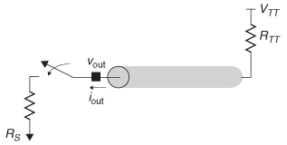
Figure 11-29 Open-drain interconnect with termination at both ends.

Figure 11-30 30 GTL transmitter circuit with analog slew rate control.
11.8 DIFFERENTIAL CURRENT-MODE TRANSMITTERS
11.8.1 Operation
Differential current-mode transmitters are often used for high-speed data transmission. In this case, the transmitter operates by injecting a current onto the transmission line. Figure 11-31a depicts a simple differential transmitter design. The transmitter uses complementary input signals, vin and ![]() in, which ensure that only one side of the circuit is in the conducting state at any given time. Thus, the transmitter uses the differential input signals to steer the current from the constant current source, iS, to the desired side of the circuit. The flow of current creates a voltage drop across the source termination resistor, RTT, on one side of the circuit, while the side that has no current flow is pulled up to VDD, thereby creating the output signal levels vout and
in, which ensure that only one side of the circuit is in the conducting state at any given time. Thus, the transmitter uses the differential input signals to steer the current from the constant current source, iS, to the desired side of the circuit. The flow of current creates a voltage drop across the source termination resistor, RTT, on one side of the circuit, while the side that has no current flow is pulled up to VDD, thereby creating the output signal levels vout and ![]() out . The relationship between input and output signals is summarized in Table 11-4. The table demonstrates that the differential signal swing has a magnitude (2iTxRTT) that is twice that of the singled-ended swing.
out . The relationship between input and output signals is summarized in Table 11-4. The table demonstrates that the differential signal swing has a magnitude (2iTxRTT) that is twice that of the singled-ended swing.
Figure 11-31 (a) Differential current mode simple transmitter design; (b) linear model.

TABLE 11-4 Relationship Between Differential Transmitter Input and Output Signals
| vin/ | ||
| Low/High | High/Low | |
| VDD/0 | 0 | VDD |
| vout | VDD | VDD - iTX RTT |
| VDD - iTX RTT | VDD | |
| vdiff = vout - | iTX RTT | - iTX RTT |
Benefits As we demonstrated in Chapter 7, differential signal transmission improves signal-to-noise ratio (SNR), which offers a path to higher data rates. Part of the reason for the improved SNR is that the differential signal swing is twice that of a single-ended signal. In addition, the differential transmitter circuit draws a nearly constant current, which drastically reduces the simultaneous switching noise (SSN). In addition, differential receivers reject the vast majority of common-mode noise. All of these factors combine to provide substantial performance headroom over single-ended signaling.
11.8.1 Modeling
As shown in Figure 11-31b, a linear model of a differential current source transmitter consists simply of a pair of complementary transient current sources connected to bias/termination transistors, along with any parasitic capacitance. Nonlinear models look similar to those for push-pull transmitters, except that the current-voltage relationships follow a saturated profile rather than the more linear characteristic of the push-pull circuit.
11.8.2 Advanced Design Considerations
In its simplest form, a current-mode transmitter is a MOSFET device operating in the saturation region (vDS ≥ vGS - vT), as shown in Figure 11-31. However, to limit the variation in output current, current-mode transmitter designs typically include additional circuitry to compensate for process and environment effects. For an example, we refer to Figure 11-32, which shows a transmitter design for use in a low-voltage differential signaling (LVDS) interface [Granberg, 2004]. The circuit contains a reference current generator on the left-hand side of the figure that is used to bias the output buffer on the right-hand side of the circuit in order to produce a tightly controlled output current. The external resistor connects to the on-die reference circuit to generate a 4-mA reference current which establishes the bias levels, vp,bias and vn,bias. The bias voltages feed the output buffer in order to produce the LVDS output swing (1.0 to 1.4 V) when connected by a 100-Ω load resistor, when the differential input signals are applied.
Figure 11-32 LVDS current mode transmitter circuit with controlled current reference. (From Gabara [1997].)

It is worth pointing out that current-mode transmission does not require differential signaling but can be applied to high-speed single-ended signals as well. Low-swing current-mode transmission systems in general provide better noise immunity and power dissipation than does voltage mode rail-to-rail signaling [Dally and Poulton, 1998]. An example of a single-ended current-mode interface is the Direct Rambus DRAM technology [Lau et al., 1998; Granberg, 2004].
11.9 LOW-SWING AND DIFFERENTIAL RECEIVERS
We treat the input receivers for low-swing and differential signaling techniques in the same section, as they both typically employ differential amplifiers, which provide fast transient response to small signal swings.
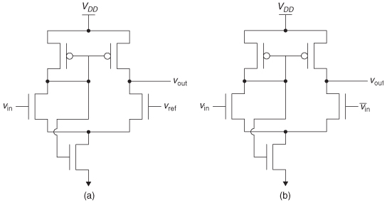
11.9.1 Operation
In principle, the differential amplifier design is the same for single-ended low-swing and differential signaling applications. In the single-ended application, one input is connected to a reference signal, vref, while the other is connected to the data signal. For differential signals, the amplifier inputs are connected to the complementary data signals. Examples of each are shown in Figure 11-33. The single-ended receiver is the original design for use with GTL signaling and was designed to switch within vref ± 50 mV across process, voltage, and operating temperature in order to provide a high noise margin with an 800-mV swing [Gunning et al., 1992]. The differential receiver is a self-biasing Chappell amplifier that uses an internal feedback signal to adjust the bias voltage for proper operation [Chappell et al., 1998].
Figure 11-33 Example receiver circuits for low-swing and differential signaling: (a) single-ended; (b) differential.
As mentioned above, differential amplifiers respond to small changes in input signals, as their symmetry gives low-input offset voltages and makes them relatively insensitive to power supply fluctuations. Differential receivers also reject common-mode noise, with typical common-mode rejection ratios (CMRRs) of -20 dB or more.
11.9.2 Modeling
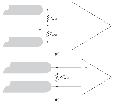
We model differential amplifier-based receivers in the same fashion as we model single-ended receivers. The simplest model is simply a capacitance to ground in conjunction with the termination. With differential signals, we have multiple options for termination, as Figure 11-34 shows. Note that the termination for differential signals is typically implemented on the silicon die, resulting in nonlinear current versus voltage characteristics that we may need to include in a behavioral model. In addition, we need to include the parasite effects and nonlinear characteristics of the ESD protection devices.
Figure 11-34 Termination options for differential signals: (a) single-ended termination; (b) differential termination.
11.9.3 Advanced Design Considerations
The examples in Section 11.9.1 are intended to illustrate the concepts, and represent only two of a wide range of choices for high-performance receiver designs. In practice, designers have multiple options for improving the various performance aspects of the receiver, such as common-mode range and input offset voltage. We refer interested readers to Dally and Poulton [1997] for more information on receiver design options and techniques.
11.10 IBIS MODELS
As we mentioned in Section 11.1, silicon suppliers do not like to provide transistor models for their I/O circuits. However, simple linear models often do not satisfy the accuracy requirements of high-speed signaling links. To meet this need, the industry has developed the I/O Buffer Information Specification (IBIS). As the name suggests, IBIS is a format for specifying I/O circuit information. Created in the early 1990s, it is now an industry standard owned by the IBIS Forum and is supported by approximately 60 companies. The diverse membership has allowed IBIS to evolve to meet the changing needs of signal integrity and I/O design engineers. In this section we give a brief overview of the IBIS standard, highlighting the major components and providing a high-level description of the model development process. The major features of IBIS include:
- Nonlinear current versus voltage curves for transmitters, ESD devices, and on-chip termination
- Separate nonlinear voltage versus time curves for transmitter pull-up and pull-down devices
- Pad capacitance for I/O circuits
- Models for minimum, typical, and maximum cases within a single model
- Description for multiple types of I/O, including differential pins, open-drain output, tristate outputs, and receivers with hysteresis
- Inclusion of signal quality specifications, including input logic thresholds, overshoots, and so on
- The Golden Parser, a tool that checks model syntax for conformance to the standard
- Backward compatibility with models created under previous revision of the standard
For further details we refer readers to the IBIS specification [IBIS, 2006] and model development “cookbook” [IBIS, 2005].
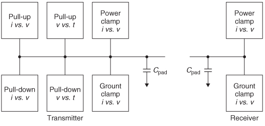
11.10.1 Model Structure and Development Process
The basic structure of an IBIS-compliant model is shown in Figure 11-35. The i - v and v -t curves are specified in table format, with columns for the minimum, typical, and maximum case. The power clamp and ground clamp tables contain both ESD clamp information and the behavior of any parasitic diodes which are part of the pull-up and pull-down transistor structures. Since the clamp circuitry is always active, the i - v data for the power and ground clamp models can be combined with the i - v data for the transmitter or receiver circuit to provide a single data table. This same property allows on-die termination resistance to be incorporated into the clamp models for transmitters and receivers, as well.
Figure 11-35 Basic structure of an IBIS model.
The development process includes four major steps [IBIS, 2005]:
1. Determine required model features, complexity, and operating range.
2. Obtain the simulated or measured model data (i - v and v -1 curves, parasitic capacitances). We treat these in more detail in subsequent sections.
3. Put it into IBIS format and check the file using the Golden Parser. This tool checks the model for syntax compliance with the IBIS standard and is available from the IBIS Forum website.
4. Validate the model. Initially, this is typically done by comparing the transient response of the IBIS model to the original transistor model when driving a reference load. Eventually, the model should be correlated against real silicon.
The data extraction and IBIS formatting can be done manually, though automated tools are available [Varma et al., 2003]. The model process works for both single ended and differential I/O, though it must be modified somewhat to handle the complementary outputs, and to extract both common mode and differential mode data, including capacitances.
11.10.2 Generating Model Data
Current Versus Voltage (i - v) Curves In constructing the i - v curves for a transmitter circuit, the output is connected to an independent voltage source, as shown in Figure 11-36. The current flow into the pad is then measured as the source is swept across a range from - VDD to 2VDD. IBIS uses the convention that current flow into the transmitter is positive. Separate curves are required for pull-up and pull-down devices. For example, the input to an inverter-based push-pull transmitter would be set to ground to obtain the curve for the pull-up device.
The circuit setup for characterizing a receiver or ESD clamp is identical except that the independent voltage source is connected to the input node. As mentioned earlier, incorporating on-chip termination in an IBIS model is accomplished by including it in the i -v curves for the clamp circuits. This can be accomplished by including it with the clamp circuit during the data extraction process or by extracting the curves separately and adding them together.
The data tables should use enough data points around sharply curved areas of the i -v characteristics to describe the curvature accurately. IBIS does not require equally spaced points in the models, so in linear regions there is no need to include unnecessary data points. Also, as Figure 11-37 demonstrates, the i - v curves for pull-ups and power clamps are VDD referenced, while pull-downs and ground clamps are referenced to ground.
Voltage Versus Time Curves Transmitter output waveforms are described with tables that specify the output voltage versus time (v -t). These v -t tables are created when the transmitter is driving into a test load, which is usually a 50-Ω resistor that is connected to the appropriate supply, as described below. The actual v -t data are generated by simulating rising and falling edges, with the output of the transmitter to each rail through the test load, as shown in Figure 11-38. For a push-pull transmitter, a minimum of four v -t curves is desired, as shown in the figure. All of the curves must be time correlated, which means that they start from the same reference point in time. By specifying the curves in this manner, IBIS models are able to capture the effects of separate switching for the pull-up and pull-down devices. This is particularly useful for modeling “break-before-make” circuits, such as the one studied in Problem 11.1, and also allows the support of “multistaged” output drivers, which are described below.
Figure 11-36 i -v curve extraction process.
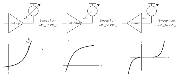
Figure 11-37 Construction of VDD relative i -v curves.
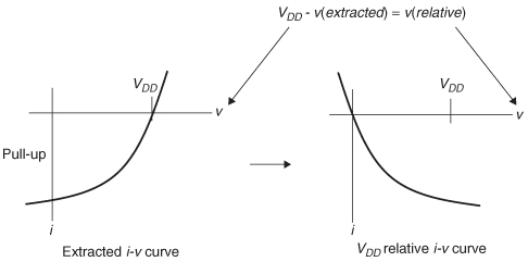
Figure 11-38 Voltage versus time curves for a push -pull IBIS model.
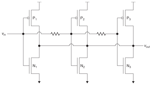
Multistage drivers control the rise and fall times of the output by spreading out switching of the pull-up and pull-down devices over time (Figure 11-39). These models break the circuit into multiple pull-up and pull-down devices, which requires multiple sets of v -1 and i - v curves to properly model the behavior of the circuit. IBIS provides a keyword to allow scheduling of the application of the multiple curves to reflect the staged switching behavior.
Figure 11-39 Multistage controlled-rise-time transmitter.
IBIS supports up to 1000 v –t points per table, and the time step used in the table should be minimized to provide maximum resolution. The test load that is used in generating the v –t tables must be described in the model. The signal integrity simulation tool will use this information from the model to reconcile the output waveform to reflect the behavior when driving the actual system load. As with the i – v curves, IBIS accommodates separate v –t curves for minimum, typical, and maximum cases.
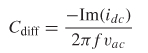
I/O Capacitance The capacitance of the I/O circuit includes the transistors, on-die interconnect, and die pad, and can have separate values for minimum, typical, and maximum cases. Designers have multiple options at their disposal for extracting the I/O capacitance values. We describe one of them here. We connect the circuit to an ac voltage source at the I/O pad so that we capture all the contributors to the capacitance, as shown in Figure 11-40. By measuring the current flow into the circuit, we can calculate the capacitance using
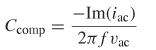
where f is the frequency of the ac source, vac is the amplitude of the source, and Im(iac) is the imaginary portion of the current flowing into the ac source.
If the I/O capacitance may be affected by the bias (dc) voltage of the circuit, we must include a dc offset in the ac source. In addition, I/O capacitance typically varies with frequency and applied voltage, so performing multiple extractions while sweeping both of those parameters is recommended. For a given model, simply choose the capacitance value that corresponds to expected switching frequency and bias voltage of the application [IBIS, 2005].
Figure 11-40 Circuit for extracting I/O capacitance.

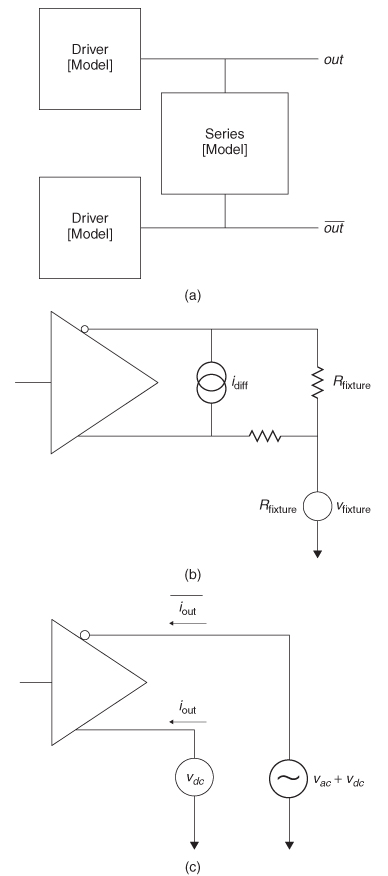
11.10.3 Differential I/O Models
The IBIS standard includes the ability to specify models for differential transceivers, although the process is more complex than for singled-ended circuits. A differential model is specified as using a driver pair along with a series model, in the manner shown in Figure 11-41a. This structure allows the models to comprehend the differential and common-mode characteristics of a differential I/O circuit. Proper modeling requires specification of the common-mode and differential-mode i -v tables. As a result, the common-mode and differential-mode currents must be must be extracted and separated. Extraction of the v -t tables uses the same techniques as for single-ended transmitters, with the addition of a current source in between the output pins to cancel differential currents inside the transistor model, as shown in Figure 11-41b. The I/O capacitance must include the differential capacitance between the two signals, as Figure 11-41c shows, with the differential and total capacitance expressed as
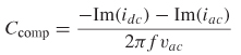
where idc is the current measured through the dc voltage source, iac is the current measured through the ac voltage source, and vac is the amplitude of the ac source. The current through the dc source will have an imaginary portion only if there is a reactive path between the two pads of the differential signal.
As a final thought, we note that multi-Gb/s differential signaling is still in the early stages of deployment and that the IBIS specification has not yet fully comprehended the needs of those high-performance links, although the standard will continue to evolve to do so in the near future.
Figure 11-41 (a) IBIS differential model structure; (b) v -t extraction fixture; (c) capacitance extraction fixture.
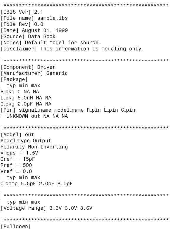
11.10.4 Example of an IBIS File
In this section we provide an example of a very basic IBIS model file, which contains a model for a push-pull transmitter. The IBIS keywords are enclosed in brackets. Note that IBIS also includes provision for specifying package information and to enable post-layout analysis by including both package and pinlist associations with buffer data, although we have elected not to specify it in this example.
11.11 SUMMARY
In this chapter we described the operation and modeling of contemporary high-speed I/O circuits, including transmitters, receivers, and on-die terminations. Insight into the behavior of these circuits is critical to designing successful high-speed signaling solutions. The signal integrity engineer who gains sufficient understanding to interact successfully with his or her I/O circuit counterpart will have a key tool for optimizing a signaling system design for high-speed operation.
REFERENCES
I/O circuit design remains an area of active research, with dozens of papers published in conference proceedings and technical journals each year. We do not attempt here to provide an exhaustive survey of the published literature. For more complete treatments of I/O and ESD circuits, we refer the reader to Dabral and Maloney [1997] and Dally and Poulton [1997]. The work by Dabral and Maloney focuses more on basic techniques, whereas Dally and Poulton offer a more comprehensive approach. Granberg [2004] compiled a comprehensive reference that includes technical data on a wide variety of I/O techniques and standards, including memory and multi-Gb/s serial links.
Boni, Andrea, Andrea Pierazzi, and Davide Vecchi, 2001, LVDS I/O interface for Gb/s-per-pin operation in 0.35-μm CMOS, IEEE Journal of Solid-State Circuits, vol. 36, no. 4, Apr., pp. 706-711.
Chappell, Barbara, et al., 1998, Fast CMOS ECL receivers with 100-mV worst-case Sensitivity, IEEE Journal of Solid-State Circuits, vol. 23, No. 1, Feb., pp. 59-67.
Dabral, Sanjay, and Timothy Maloney, 1998, Basic ESD and I/O Design, Wiley-Interscience, New York.
Dally, William, and John Poulton, 1998, Digital Systems Engineering, Cambridge University Press, Cambridge, UK.
Esch, Gerald, Jr., and Tom Chen, 2004, Near-linear CMOS I/O driver with less sensitivity to process, voltage and temperature variations, IEEE Transactions on Very Large Scale Integration Systems, vol. 12, no. 11, Nov.
Gabara, Thaddeus, and Scott Nauer, 1992, Digitally adjustable resistors in CMOS for high performance applications, IEEE Journal of Solid-State Circuits, vol. 27, no. 8, Aug., pp. 1176-1185.
Gabara, Thaddeus, and David Thompson, 1998, Ground bounce control in CMOS integrated circuits, Proceedings of the 1988 IEEE International Solid-State Circuits Conference , pp. 88-90.
Gabara, Thaddeus, et al., 1997, LVDS I/O Buffers with a Controlled Reference Circuit, IEEE Publ. 1063-0988/97, IEEE Press, Piscataway, NJ, pp. 311-315.
Granberg, Tom, 2004, Digital Techniques for High-Speed Design, Prentice Hall, Upper Saddle River, NJ.
Gunning, Bill, et al., 1992, A CMOS low-voltage-swing transmission-line transceiver, Proceedings of the 1992 IEEE International Solid-State Circuits Conference, pp. 58 -59.
Hall, Stephen, Garrett Hall, and James McCall, 2000, High-Speed Digital System Design, Wiley-Interscience, New York.
IBIS Open Forum, 2005, IBIS Modeling Cookbook for IBIS Version 4.0, http://www.eigroup.org/ibis/, Sept. 15.
IBIS Open Forum, 2006, IBIS (I/O Buffer Information Specification), Version 4.2, http://www.eigroup.org/ibis/, June.
Intel Corporation, 2002, AGP V3.0 Specification, revision 1.0, Intel Press, Hellsboro, OR, Sept.
Intel Corporation, 2005, 64-Bit Intel® XeonTMProcessor with 2MB L2 Cache, Document 306249-002, Intel Press, Hillsboro, OR, Sept.
Lau, Benedict, et al., 1998, A 2.6-Gbyte/s multipurpose chip-to-chip interface, IEEE Journal of Solid-State Circuits, vol. 33, no. 11, Nov., pp. 1617-1626.
Rabaey, Jan, Anantha Chandrakasan, and Borivoje Nikolic, 2003, Digital Integrated Circuits: A Design Perspective, 2nd ed., Prentice Hall, Upper Saddle River, NJ.
Synopsis, Inc., 2006, HSPICE>® Simulation and Analysis User Guide, Version Y-2006.3, Synopsis, Mountain View, CA, Mar.
Texas Instruments, 1996, The Bergeron Method: A Graphic Method for Determining Line Reflections in Transient Phenomena, Document SDYA014, Texas Instruments, Dallars, TX, Oct.
Varma, Ambrish, et al., 2003, The development of a macro-modeling tool to develop IBIS models, Proceedings of the IEEE 12th Topical Meeting on Electrical Performance of Electronic Packaging, Oct. 27-29, pp. 277-280.
Wang, Niantsu, 1989, Digital MOS Integrated Circuits, Prentice Hall, Upper Saddle River, NJ.
PROBLEMS
Use the device parameters in Table 11-5 when solving these problems.
TABLE 11-5 Device Parameters for a 0.25 μm Process
Source: Rabaey et al. [2003].
| NMOS | PMOS | |
| VTo0 (V) | 0.43 | -0.4 |
| γ(V½) | 0.4 | -0.4 |
| VD,SAT (V) | 0.63 | -1 |
| k (A/V2) | 115 × 10-6 | -30 × 10-6 |
| λ (V-1) | 0.06 | - 0.1 |
11-1 Describe operation of the break-before-make circuit shown in Figure 11-42.
Figure 11-42 Break-before-make push-pull transmitter circuit.

11-2 Construct the i - v curve(s) and use them to calculate output impedance for the push-pull transmitter shown in Figure 11-43.
11-3 Explain how the staged circuit in Figure 11-39 provides a controlled rise time at the output of the circuit. Sketch the output waveform expected.
11-4 Describe the operation of the Schmitt trigger receiver shown in Figure 11-14.
11-5 Use a Bergeron diagram to analyze the falling-edge response of the circuit in Figure 11-18.
11-6 Use a Bergeron diagram to analyze the rising edge for the circuit shown in Figure 11-44.
Figure 11-43 Push-pull transmitter for Problem 11-2.
Figure 11-44 Diode-terminated circuit for Problem 11-6.

11-7 Describe how the GTL transmitter circuit shown in Figure 11-30 slows the rising-edge transition to reduce ringing due to parasitic package inductance.
11-8 Use a Bergeron diagram to analyze the far-end-terminated open-drain circuit in Figure 11-45.
11-9 Analyze the two open-drain circuits in Figure 11-45. How do the resulting waveforms differ? Which is likely to be capable of supporting a higher data transfer rate?
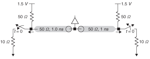
11-10 Wired-OR glitch: The circuit in Figure 11-46 contains transmitters at each end, with a receiver circuit near the middle. Initially, the right-hand transmitter pulls the circuit low while the transmitter on the left is turned off. At time t = 0 the left-hand transmitter turns on and the right-hand transmitter turns off. Sketch the waveform at the receiver.
11-11 Use the device parameters in Table 11.5 to calculate the current versus voltage curve for the on-die termination circuit shown in Figure 11-47 and estimate the effective termination resistance.
Figure 11-45 Open-drain circuits for Problem 11-8.
Figure 11-46 Wired-OR circuit for Problem 11-10.
11-12 Discuss the potential advantages and disadvantages of the single-ended and differential termination schemes shown in Figure 11-34.
Figure 11-47 FET termination circuit for Problem 11-11.

11-13 Complete a Bergeron diagram using the transmitter and receiver load lines shown in Figure 11-48, which are used in conjunction with a 70-Ω transmission line.
Figure 11-48 Load lines for Problem 11-13.
