
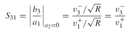
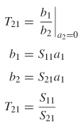
9
NETWORK ANALYSIS FOR DIGITAL ENGINEERS
9.1 High-Frequency Voltage and Current Waves
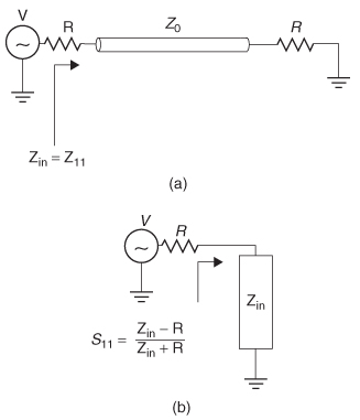
9.1.1 Input Reflection into a Terminated Network
9.1.2 Input Impedance
9.2 Network Theory
9.2.1 Impedance Matrix
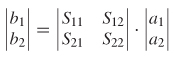
9.2.2 Scattering Matrix
9.2.3 ABCD Parameters
9.2.4 Cascading S–Parameters
9.2.5 Calibration and De–embedding
9.2.6 Changing the Reference Impedance
9.2.7 Multimode S–Parameters
9.3 Properties of Physical S-Parameters
9.3.1 Passivity
9.3.2 Reality
9.3.3 Causality
9.3.4 Subjective Examination of S–Parameters
References
Problems
Historically, the techniques used to analyze signal integrity for digital designs required the use of equivalent circuits to describe components such as vias, connectors, sockets, and even transmission lines for low–data–rate applications. At low frequencies where the interconnects between the components of a digital system are small compared to the wavelength of the signal, the circuits can be described with lumped elements using resistors, capacitors, and inductors. In general, circuit theory works well for these types of problems because there is negligible phase change in the voltage and current across the circuit. In other words, the signal frequency is low enough so that the electrical delay of the circuit is small compared to the switching rate of the digital waveforms. However, as system data rates increase, the delay of the interconnects becomes significant. In fact, in many modern digital designs, such as in high–speed computers, the delay of the system interconnects is so long compared to the width of a single bit of digital information that many bits can be propagating on the bus simultaneously. In this case, the phase changes of the voltage and current across the interconnects are very significant. As a result, digital engineers have turned to new techniques for describing and analyzing circuits at high frequencies, called network analysis.
Network analysis is a method used traditionally by microwave and radiofrequency engineers to characterize devices such as waveguides, cables, couplers, and antennas. They are used to describe completely the behavior of linear time–invariant systems using only parameters evaluated at the input and output ports. Network analysis is a frequency domain methodology that allows discrete characterization of a linear network at each frequency. The question often arises: Why would a digital engineer use frequency–domain analysis when a digital system uses time–domain pulses? The answer is simple: It is often easier to analyze and characterize systems in the frequency domain. In Chapter 8 we discussed methods to describe a system in terms of its impulse response. Although this is a fine theoretical concept, the problem remains that it is impossible to create or measure a true impulse physically. Furthermore, as described with equation (8-10), the impulse response can be calculated from the transfer function, which is a measurable frequency–domain parameter. Additionally, many of the concepts described in the book, such as skin effect resistance and loss tangents, are best analyzed in the frequency domain. In fact, the validity of a model in the time domain is sometimes judged using frequency–domain techniques, as described in Section 8.2. In short, network analysis is a useful tool for characterizing system interconnects, specifying component performance and creating portable, tool–independent models.
Although general network theory is presented in this chapter, the main area of concentration will be on the derivation and use of the scattering matrix, more commonly known as S–parameters. S–parameters are quickly gaining acceptance in the electronics industry for specifying the performance of digital components such as transmission lines, CPU sockets, and connectors. Furthermore, methodologies have developed that allow the use of S–parameters as a portable “black box” model that can be included in the simulation environments of several commercial tools. The problem is that most digitally oriented engineers are not familiar with the concept of network theory or S–parameters because it is traditionally taught in microwave, electromagnetic interference, or radio engineering curricula. In this chapter we discuss the applications and usage models of network analysis that are most applicable to the design and validation of high–speed digital systems.
9.1 HIGH–FREQUENCY VOLTAGE AND CURRENT WAVES
As a prerequisite to describing network theory, it is required to understand how voltage and current waves propagating on an interconnect will interact with different loads. Many of these concepts were covered partially in Chapter 3 when lattice diagrams and the reflection coefficient at an impedance junction were discussed. In this chapter we build on those concepts to calculate the reflection coefficient looking into a network, such as a transmission line terminated in a load that is not equal to the characteristic impedance. Similarly, the impedance looking into a terminated network is also calculated. These concepts are important for the development of network theory.
9.1.1 Input Reflection into a Terminated Network
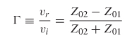
The reflection coefficient looking into a network with a finite electrical length is different from the reflection coefficient looking into an impedance junction because it has a phase component that will change with electrical length and frequency. Equation (3-102) from Section 3.5.1 defines the reflection coefficient looking into an impedance junction:
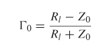
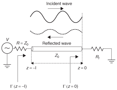
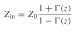
where vr and vi are the reflected and incident voltage values, respectively. In the case of equation (3-102) the reflection occurs immediately, so there is zero phase delay between the incident and reflected waves. However, consider the case shown in Figure 9-1, where there is a significant distance between the point where the reflection is being evaluated and the impedance discontinuity. The reflection coefficient at the load, Γ(z = 0), can be calculated with equation (3-102):
However, consider Γ(z = –l), which is the reflection coefficient looking into the input of the network. After a signal is driven onto the network, the reflection will not arrive back at the input until the signal propagates down the network, reflects off the impedance discontinuity at z = 0 (defined by Γ0), and propagates back to the source. Depending on when the reflections arrive at the receiver, the incident and reflected waves will combine at specific frequencies and interact either constructively or destructively. If the incident and reflected waves interact destructively, the reflection coefficient will be minimized (and vice versa). This means that the reflection coefficient looking into the network will be influenced by propagation delay, characteristic impedance, termination impedance, length, and frequency.
Figure 9-1 The reflection looking into a network is dependent on the distance between the point where the reflection is being evaluated and the impedance discontinuity.
The reflection coefficient looking into a network can be derived from equations (6–49) and (3–102):

where
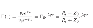
Equation (9-1) describes the reflection coefficient looking into a transmission line with characteristic impedance Zo, length z, termination impedance Rl, and propagation constant γ.
In Section 3.5 the concept of lattice diagrams was introduced to demonstrate how time–domain signals propagate on transmission lines. An important concept demonstrated was that the period of transmission–line “ringing” was dependent on the electrical length of the line. In frequency–domain analysis, the same principles apply; however, it is more useful to calculate the frequency when the reflection coefficient is either maximum or minimum, which is dependent on both the electrical length of the structure and the frequency of the input stimulus. To demonstrate this concep
(3-29)![]()
(3-30)![]()
Beginning with equation (9-1), the reflection coefficient looking into a terminated transmission line with a length of –l is calculated and expanded using equation (2-31):
where a negative length convention is chosen for convenience.
Since the real and imaginary parts of (9–2) are periodic, the frequencies where the function is only real or imaginary can be calculated. The reflection looking into a nonperfectly terminated transmission line is purely imaginary when ![]() for odd n because it will force the cosine term to be zero. Solving for the frequency where the reflection is imaginary produces
for odd n because it will force the cosine term to be zero. Solving for the frequency where the reflection is imaginary produces
Similarly, the frequencies where equation (9-2) is purely real can be calculated for the conditions where the sine term is zero:![]() . The frequency where the reflection is real is shown by
. The frequency where the reflection is real is shown by
Equations (9–3) demonstrate that when the real part of the input reflection is zero, the imaginary portion is maximum, and vice versa, as plotted in Figure 9-2. This periodic behavior can be used to extract out useful information about the device under test.
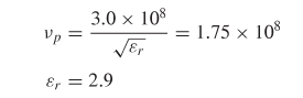
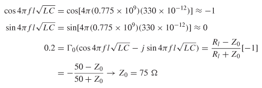
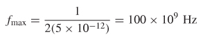
Example 9–1 Calculate the propagation delay, characteristic impedance, and the dielectric permittivity from the input reflection coefficient plot in Figure 9-2, assuming a circuit similar to Figure 9-1 with a length of 2.28 in. (0.058 m) and termination impedance Rl of Ω
SOLUTION
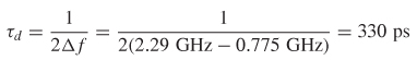
Step 1: To begin, consider the real portion of Figure 9-2. According to equation (9-3b), the frequencies will be purely real at multiples of n. Examination of Figure 9-2 shows that the period of the real portion can be measured at 0.775 and 2.29 GHz. Since these peaks are the first and the third frequencies, where the reflection coefficient is purely real, they correspond to n = 1 and n = 3. Using equation (9-3b) and subtracting produces an equation in terms of the frequency difference between positive real peaks and the electrical delay:
Figure 9-2 When the real part of the reflection coefficient looking into a network is maximum, the imaginary part is zero.
where ![]() , from equation (3-107). Therefore, the propagation delta can be calculated:
, from equation (3-107). Therefore, the propagation delta can be calculated:
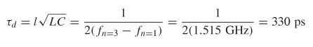
Note that the propagation delay calculated using this technique is the average value between 0.775 and 2.29 GHz. Due to the frequency dependence of the dielectric permittivity described in Chapter 6, the actual value actually changes across the bandwidth.
Step 2: To calculate the dielectric permittivity, the propagation delay must first be translated into a velocity:
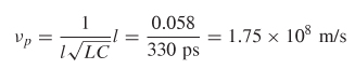
Next, equation (2-52) with fir – 1 is used to calculate the relative dielectric permittivity.
Step 3: Calculate the characteristic impedance using the peak values of the reflection coefficient. When the imaginary term is zero, the real term will peak because the cosine term of equation (9-2) will equal 1 at frequencies predicted by (9–3b). Therefore, the easiest way to calculate the characteristic impedance is to use the value of the reflection coefficient measured at a real peak.
The first real peak at 0.775 GHz shows a maximum reflection coefficient of 0.2. The characteristic impedance can be calculated by setting the reflection coefficient equal to equation (9-2) at 0.775 GHz and solving for Z0.
Step 1 in Example 9–1 demonstrates a very useful relationship between the periodicity of the input reflection coefficient looking into a network and the
propagation delay. If the distance between peaks (fn=3 – fn=1) is represented as Δf and ![]() the time delay can be calculated using
the time delay can be calculated using

The utility of equation (9-4) will become apparent when analyzing S–parameters in Section 9.2.2.
In summary, the reflection coefficient looking into a network is dependent on (1) the impedance discontinuities, (2) the frequency of the stimulus, and (3) the electrical length between discontinuities.
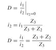
9.1.2 Input Impedance
Not surprisingly, if the reflection coefficient looking into a network is a function of length, impedance discontinuities, and frequency, the input impedance looking into the network must be a function of the same variables. Following a procedure similar to that used to derive equation (9-1), the impedance looking into a transmission line of length z terminated with Rl, as depicted in Figure 9-1, is easily derived, where Γ(z)is equated with equation (9-1):
Figure 9-3 Impedance looking into a 75–Ω 2.28–in. transmission line terminated in 50 Ω. Zin varies significantly with frequency due to the constructive and destructive combinations of the input stimulus and the reflected waves.
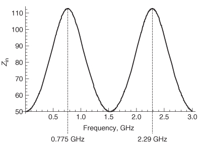
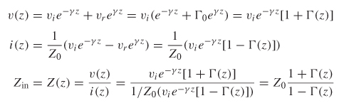
Figure 9-3 shows the input impedance as a function of frequency for the terminated transmission line in Example 9–1. Note that although the characteristic impedance and the termination value are constant, the input impedance varies significantly with frequency, due to the constructive and destructive combinations of the input stimulus and the reflected waves. At frequencies where the reflection is real and the imaginary term is zero, the reflected wave is aligned with the incident wave, causing the input impedance to peak.
9.2 NETWORK THEORY
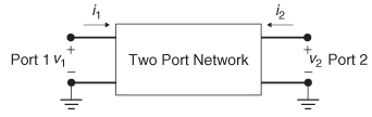
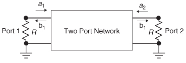
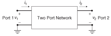
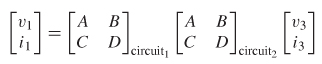
Network theory is based on the property that a linear time–invariant system can be characterized completely by parameters evaluated only at the input and output ports, without regard to the contents of the system. This allows the behavior of a system to be described fully in a frequency–dependent matrix that relates input stimuli to the output responses of the system. Networks can have any number of ports; however, consideration of a two–port network is sufficient to explain the theory. The discussion begins with the most intuitive method of describing a network, which is the impedance matrix.
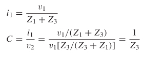
9.2.1 Impedance Matrix
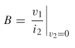
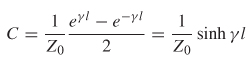
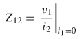
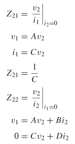
Consider the two–port network depicted in Figure 9-4. If the voltage and current are measured at the input and output ports, the system can be characterized in terms of its impedance matrix. The impedance from port 1 to port 2 is calculated by measuring the open–circuit voltage at port 2 when current is injected into port 1:
Similarly, the input impedance looking into port 1 is measured by injecting current into port 1 and measuring the voltage at port 1:
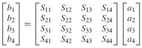
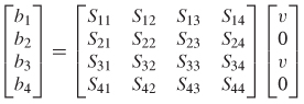
Using the definition shown in equations (9–6a) and (9–6b), a set of linear equations can be written to describe the network in terms of its port impedances:
which is expressed more efficiently in matrix form:
More generally, the elements of an impedance matrix are described in equation (9-8) for an arbitrary number of ports,
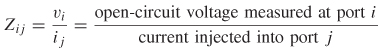
Figure 9-4 Two–port network used to generate the impedance matrix.
with ik = 0 for all k ≠ j. If the impedance matrix of a system is known, the response of the system can be predicted for any input.
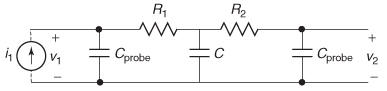
Example 9–2 Calculate the impedance matrix at 1 GHz for the circuit shown in Figure 9-5a, where R1 = 50 Ω, R2 = 50 Ω, and C = 5 pF.
SOLUTION
Step 1: Calculate the input impedance (Zn) by injecting a current into port 1 and measuring the voltage at port 1, as shown in Figure 9-5b. The impedance of the capacitor at 1 GHz is Zc= 1/j2πfC = 31.8 Ω.
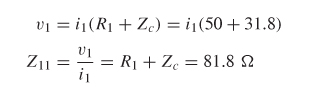
Step 2: Calculate the through impedance (Z21) by injecting a current into port 1 and measuring the voltage at port 2, as shown in Figure 9-5c.
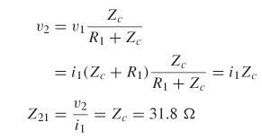
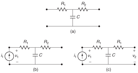
Step 3: Construct the impedance matrix at 1 GHz. Since the circuit is symmetrical, Z12 = Z21 and Z22 = Z11.
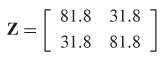
Figure 9-5 (a) General circuit to be analyzed in Example 9–2; (b) calculating Z 11 n; (c) calculating Z 21.
The admittance matrix is very similar to the impedance matrix except that it is characterized with short–circuit currents instead of open–circuit voltages. The admittance matrix is the inverse of the impedance matrix:
Although the impedance and admittance matrices are intuitive and relatively easy to understand, they have severe drawbacks for the high–frequency characterization of interconnects. The problem is that at high frequencies, open and short circuits are very difficult to realize. Open circuits invariably have finite capacitances, and short circuits have inductance that can significantly affect the accuracy of the measurements. Consequently, as a measurement technique, these methods are applicable only for low frequencies.
Example 9–3 Calculate Z21 for the circuit analyzed in Example 9–2, assuming that the current was injected into port 1 and the voltage was measured at port 2 with a probe that has a capacitance of C = 0.3 pF, according to the instrument specifications.
SOLUTION
Step 1: Draw the equivalent circuit of the circuit and the probes, as depicted in Figure 9-6. From Example 9–2, R1 = 50 Ω, R2 = 50 Ω, C = 5 pF, and Zc = 1/j 2πfC = 31.8 Ω. The impedance of the probe at 1 GHz is
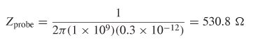
Step 2: Solve the circuit for Z11 and Z21:
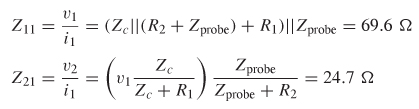
where = Z11i1. Since the circuit is symmetrical, Z12 = Z21 and Z22 = Z11.
Figure 9-6 Equivalent circuit used for Example 9–3 showing probe capacitance.
Step 3: Compare the matrix measured with a realistic probe to the ideal case:
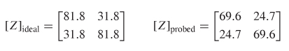
Note that even for a relatively low capacitance value of the probe, it makes a significant difference in the impedance matrix. This is because the voltage measured at port 2 is not across an open circuit; it is across a small capacitance. The fact is that at high frequencies, true short and open circuits do not really exist for small dimensions. There will always be a certain amount of parasitic capacitance or inductance with finite impedance.
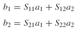
9.2.2 Scattering Matrix
In the previous section we discussed some of the problems associated with measuring high–frequency voltage and current waves, where short and open circuits do not practically exist due to parasitic inductance and capacitance values. The scattering matrix is the most common form of network parameters used in high–speed digital design. Instead of measuring voltages and currents at the ports, it relates the power waves incident on each port to those reflected from the ports. The scattering matrix, more commonly known as S–parameters, can be measured in the laboratory using a vector network analyzer (VNA). Once the S–parameters are known, conversion to other matrix parameters, such as the impedance or admittance matrices, can be done algebraically.
Traditionally, S–parameters have been a tool used primarily by microwave and RF engineers to design antennas, waveguides, and other high–frequency narrowband applications. Higher speed data transmission on system buses is causing a convergence of two disciplines in industry today: microwave and digital engineering. Microwave engineers tend to concentrate mostly on high–frequency multi–GHz waveguides, resonators, and couplers, whereas digital engineers concentrate on binary signaling. Over the past decade, S–parameters have become much more common in the world of digital design and are often used for the dissemination of electrical models to design teams. In fact, most contemporary software suites used to design modern systems have built–in capabilities to handle S–parameter models.
S–parameters can be very confusing, as unlike the impedance matrix, they are not intuitive. In this chapter we focus on the most important aspects of S–parameters that the digital engineer needs for signal integrity analysis of modern, high–speed buses. Emphasis is given to both the theoretical development of S–parameters and intuitive techniques that will allow the engineer to interpret data quickly, share models, and estimate channel performance.
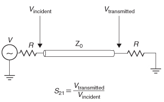
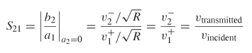
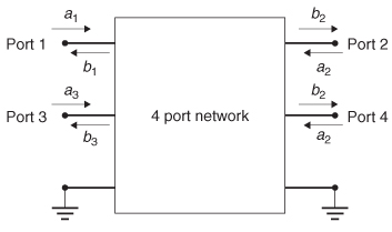
Definition Consider the two–port network in Figure 9-7. If a power wave is injected into port 1, the power must either be reflected back toward port 1, propagate through the network to port 2, or be dissipated as thermal or radiation
Figure 9-7 Two–port model used to define S–parameters.
losses. Similar to the derivation of the Poyting vector in Section 2.6, the power balance equation can be expressed as
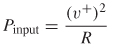
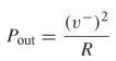
where Pinput is the total power injected into all ports, Pout is the total power flowing out of all ports, Ploss is the power dissipated through ohmic losses (skin effect, loss tangent, etc.), and Pradiated is the power radiated into free space.
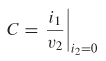
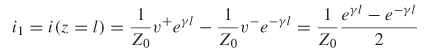
The incident and reflected power waves are calculated from voltage and current waves. The voltage waves are obtained from equation (6-49),
![]()
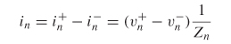
and the current wave is derived by dividing the voltage wave by the characteristic impedance of the structure,
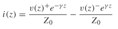
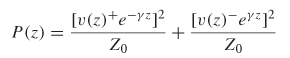
where v(z)+ is the voltage traveling in the +z–direction and v(z)– is the voltage traveling in the –z–direction. The power wave propagating on the network is calculated by multiplying the current and voltage waves:
If it is defined so that at port j, z = 0, the voltage at a port can be calculated where v(0) = vi and i(0) = ii, which are the incident voltage and current, respectively:
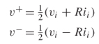
where R is the termination values at the ports of the network.
Since equation (9-10) says that the power must be balanced, the amount of power delivered to the network or radiated is defined simply as the input power minus the output power:
![]()
From equation (9-12), the power going into a node can be calculated using the power relation P = v2/R:
and the power coming out can be calculated as
meaning that the power delivered to the network is calculated as
Equations (9–13) allow the definition of terms that describe the power wave propagating into port j and the power wave propagating out of port j:
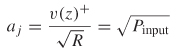
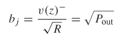
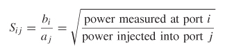
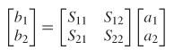
where aj is the square root of the power propagating into port j and bj is the square root of the power propagating out of port j, as shown in Figure 9-7 for a two–port network. Equations (9–14a) and (9–14b) are known as the scattering coefficients. Since they are defined in terms of the square root of power, ratios of the scattering coefficients simplify into ratios of voltage as long as the termination impedance of each port (R) is the same.
S–parameters are derived from the ratios of scattering coefficients. For example, referring to Figure 9-7, the term S11 is calculated by the root of the reflected and incident power ratio at port 1, which is written in terms of the scattering coefficients:
Similarly, the term S21 is calculated by injecting power into port 1 and measuring at port 2.

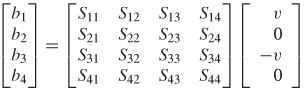
Using the definition shown in equations (9–15a) and (9–15b), a set of linear equations can be written to describe the network in terms of its scattering coefficients:
![]()
which is more efficiently expressed in matrix form as
More generally, the elements of a scattering matrix are described in equation (9-17) for an arbitrary number of ports,
and an arbitrary–sized scattering matrix takes the form
If the scattering matrix of a system is known, the response of the system can be predicted for any input.
Return Loss Consider the circuit depicted in Figure 9-8. In this case there will be no reflections from the far end because the line is perfectly terminated with the characteristic impedance. However, the source impedance is not equal to the characteristic impedance, indicating that a portion of the power wave incident to port 1 will be reflected. This scenario allows the simplest definition of S11, which is simply the reflection coefficient between the source resistor and the impedance of the transmission line. Note that a2 = 0 because there is no source at port 2.
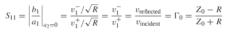
The term S11 is often referred to as the return loss, because it is a measure of power reflected, or returned to the source.
The calculation of S11 becomes more complex when the far end of the network is not perfectly terminated because the reflection arriving at the source will have
Figure 9-8 Return loss for the special case when the network is perfectly terminated in its characteristic impedance.
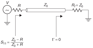
Figure 9-9 Return loss for the more general case where the network is not perfectly terminated in its characteristic impedance: (a) input impedance looking into the network; (b) equivalent circuit for the return loss.
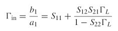
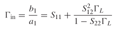
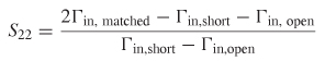
contributions from both the impedance discontinuity at the source and at the far–end termination. This means that the input impedance looking into the network from the source will be dependent on frequency. The return loss for a nonperfectly terminated structure such as the circuit shown in Figure 9-9a is calculated as
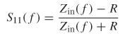
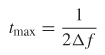
where Z–in(f ) is calculated for a transmission line with equation (9-5) for the general case. An intuitive understanding of the return loss can be achieved by constructing a simple equivalent circuit as shown in Figure 9-9b. Since Zin (or Z11) is dependent on both the propagating delay and the impedance of the structure, both can be calculated from S11, as demonstrated in Example 9–4.
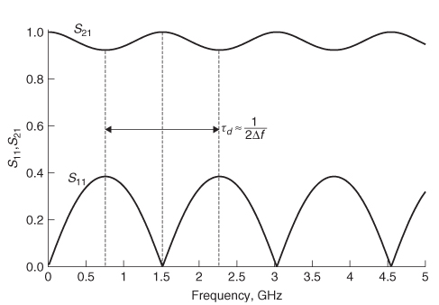
Example 9–4 Using the measured return loss of a transmission line shown in Figure 9-10, calculate the characteristic impedance and the propagation delay. Assume that the source and termination impedance values are 50 Ω
SOLUTION
Step 1: Determine the propagation delay. This is easily calculated from the periodic behavior of S11 using equation (9-4). The distance between peaks is
Figure 9-10 Return loss (S 11) for Example 9–4.
used to calculate Δf.
Note that τd is the average propagation delay over the frequency range.
Step 2: Calculate the input impedance using equation (9-20). When the return loss (S11) is maximum, the imaginary part is zero. Therefore, it is convenient to measure S11 at a peak to simplify the analysis:
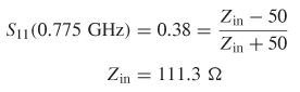
Step 3: Determine the polarity of the phase term. The polarity of the phase term e2γz in equation (9-1) must be determined so that the input impedance can be properly related to the characteristic impedance. Since S11 is being evaluated at a peak, the imaginary term of e2γz is zero, so the real part will either be 1 or – 1. Since the propagation delay has been calculated, the polarity of the phase term can be evaluated using the real part of equation (9-2):
Step 4: Calculate the characteristic impedance from equation (9-5):
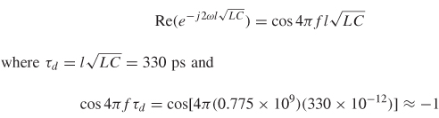
Since the phase term calculated in step 3 is –1, the input reflection coefficient at 0.775 GHz is calculated from equation (9-1) with e2γz= –1:
Insertion Loss When power is injected into port 1 and measured at port 2, the square root of the power ratio reduces to a voltage ratio. S21, the measure of the power transmitted from port 1 to port 2, is called the insertion loss :
which is shown in Figure 9-11 for a transmission line. In digital system design, the insertion loss is the most commonly used parameter of the scattering matrix because it is a measure of both delay and amplitude as seen at the receiving agent.
Figure 9-11 Insertion loss (S 21) of a transmission line.
The frequency–dependent delay can be calculated from the phase of the insertion loss,
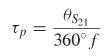
where
Note that equation (9-22), called the phase delay, has a slightly different meaning than that of the propagation delay of a digital pulse on a transmission line. Since a digital pulse is composed of numerous harmonics, and realistic dielectrics have values that vary with frequency, the propagation delay of a time–domain pulse will have numerous frequency components, each propagating with a unique phase velocity. The propagation delay of a digital pulse can be thought of as a group of harmonics propagating simultaneously and is sometimes called the group delay . The phase delay, as described with (9–22), is associated with only a single frequency.
Figure 9-12a shows an example of the phase of S21 for a 1–in. transmission–line model constructed with a realistic frequency–dependent dielectric, as described in Chapter 6. To calculate the phase delay, the phase must be unwrapped, as shown in the figure. Figure 9-12b is the phase delay calculated from the unwrapped phase using equation (9-22). Note the frequency–dependent nature of the delay, which is required for a causal transmission–line model.
For a loss–free network, the total power exiting the N ports must equal the total incident power. This means that for a two–port loss–free network, the power transmitted from port 1 to port 2 plus the power reflected from port 1 must be conserved:
Essentially, equation (9-24) says that if the power is not transmitted from port 1 to port 2, it must be reflected. This allows us to write an equation that relates the
Figure 9-12 (a) Phase of the insertion loss (S 21) for a 1–in. causal transmission line model; (b) phase delay.
Figure 9-13 Insertion and return loss for a 2–in. loss–free transmission line.
insertion loss and the return loss for a loss–free system†:
where S*iJ represents the complex conjugate of the term. Since SiJ is the square root of power measured at port i and injected at port j, the power ratio is S2iJ. However, since power is a real quantity, the squaring function is replaced with the complex conjugate to ensure that the imaginary part is zero.
Figure 9-13 shows the insertion and return loss for the loss–free transmission line used in Example 9–4 terminated with 50–Ω reference impedances. Note that when the return loss (S11) peaks, the insertion loss (S21) dips, as described by (9–25). Since the imaginary part is zero when the terms peak and the real part is zero when the terms dip, it is easy to show that the power is conserved when the insertion loss is maximum and the return loss is minimum simply by squaring the terms, which is equivalent to the complex conjugate for these conditions. For example, at the first S11 peak,
![]()
which proves that power is conserved.
For the realistic case where the transmission line is lossy, an extra term, Ploss, is added to the power balance equation to account for conductor, dielectric, and radiation losses:
Therefore, equation (9-25) can be rewritten to account for finite power losses:
Figure 9-14 shows an example of the insertion and return losses for a lossy transmission line. The power absorbed by the network can be calculated using (9–27). At the first peak (770 MHz),
![]()
meaning that the power absorbed by the system or radiated into space is 1 – 0.970 = 0.03, or 3% of the total power. Of course, the absorbed power percentage will increase with frequency because both skin effect resistance and dielectric losses increase. For example, at 5.25 GHz, the total power absorbed by the network is 9.6%.
Since properly designed transmission lines are very inefficient radiators, it is a valid assumption that very little or none of the power loss is due to radiation into free space. Of course, if there is significant coupling (crosstalk) to adjacent structures, the power will be affected, which is covered in the next section.
Figure 9-14 Insertion and return loss for a 2–in. lossy transmission line.
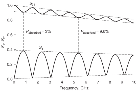
Figure 9-15 Two–transmission–line system for evaluating crosstalk using S–parameters.
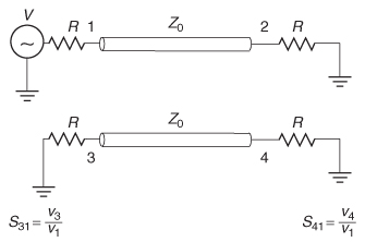
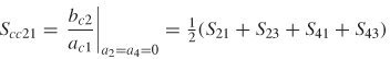
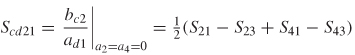
Forward (Far–End) Crosstalk When power is injected into port 1 and measured at port 4, as shown in Figure 9-15, it is called forward crosstalk, as described in Chapter 4 and defined by
Note that forward crosstalk is often called far–end crosstalk. As detailed in Section 4.4, any bit pattern propagating on a bus with N signal conductors can be decomposed into N orthogonal modes. Section 4.4.2 describes how each mode will have a unique impedance and velocity. If a two–signal conductor system is considered, such as that shown in Figure 9-15, all digital bit patterns will be a linear superposition of the even and odd modes, which are described in Section 4.3.
In Section 4.4.4, forward crosstalk for a two–signal conductor system was shown to be caused by the difference in propagation velocity between the even and odd modes. This knowledge can be used to predict the general behavior of the forward crosstalk in the frequency domain. To begin, consider the magnitude of S41 for a pair of coupled transmission lines, as shown in Figure 9-15. Using the concept of modal analysis, where the driving signal is decomposed into one–half even mode and one–half odd mode, the launch voltages at ports 1 and 3 can be constructed. For the case where port 1 is being driven with a signal and port 3 is quiet, the evenand odd–mode components are in phase at port 1 and 180° out of phase at port 3 and shown in Figure 9-16. Consequently, the sum of the modal voltages equals the driving voltage at port 1 and zero at port 3.
If the transmission–line pair is constructed with a homogeneous dielectric, the evenand odd–mode propagation velocities are identical and will therefore arrive at the far end simultaneously. In this case, forward crosstalk will be zero because the oddand even–mode components propagating on line 2 will still be 180° out of phase at node 4. However, if the transmission line is constructed with a nonhomogeneous dielectric such as a microstrip, the even and odd propagation
Figure 9-16 Modal decomposition of launch voltages when port 1 is driving as shown in Figure 9-15.
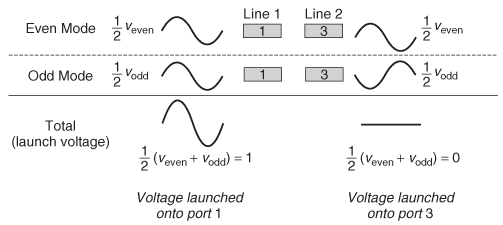
Figure 9-17 Modal decomposition of voltages at node 4 when port 1 is driving, showing that the oddand even–mode components of the signal arrive at different times when the dielectric media is nonhomogeneous, causing forward crosstalk to be finite.
velocities will differ. Therefore, the odd and even components of the signal will arrive at node 4 at different times and will no longer be 180° out of phase. Consequently, for a nonhomogeneous dielectric, the forward crosstalk will be finite, as depicted in Figure 9-17. The propagation delay of the mode is calculated from the modal velocities using equation (4-81):
where the phase delay per unit length is simply τp = 1/νp. This means that the magnitude of the forward crosstalk is dependent on the difference in delay between the odd and even modes. Since equation (9-22) relates the delay to the phase, if the velocity of each mode is known, the frequency where the phase difference between the odd and even modes is 180° can be calculated:
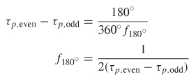
When f = f180°, the oddand even–mode voltage components will be perfectly out of phase on line 1 and in phase on line 2, which is the opposite of the launch conditions as depicted in Figure 9-18. This means that at f180°, S21 = 0 and S41 = 1, and the coupling to the adjacent line is 100%.
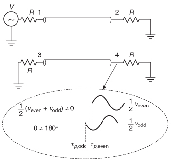
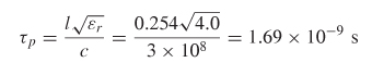
Example 9–5 Calculate the frequency where the insertion loss is minimum and the forward crosstalk is maximum for a 10–in. loss–free transmission line where εeff,even = 4.0 and εeff,odd = 3.5 for the circuit shown in Figure 9-15.
SOLUTION
Step 1: Calculate the propagation delay for the odd and even modes where 10 in. = 0.254 m and c = 3 x 10⁸m/s:
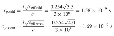
Step 2: Calculate the frequency where the phase delay between odd and even modes is 180°:
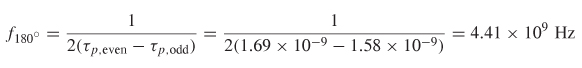
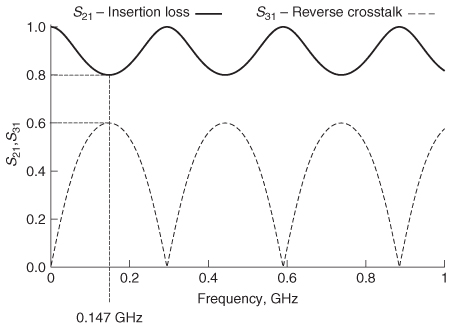
At 4.41 GHz, the insertion loss (S21) will be minimum and the forward crosstalk (S41) will be maximum. A simulation of this case is shown in Figure 9-19 for a 10–in. pair of coupled transmission lines withεeff,even = 4.0,εeff,odd = 3.5, Zodd = 25 Q, and Zeven = 100 Ω.
Figure 9-18 Modal decomposition of voltages at nodes 2 and 4 when port 1 is driving, showing that at f = f180° the insertion loss (S21) is zero and the forward crosstalk (S41) is maximum. At this frequency, the coupling to the adjacent line is 100%.
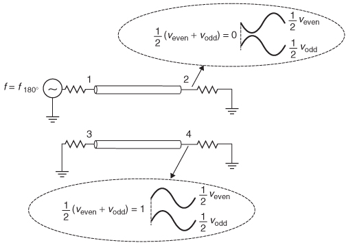
Figure 9-19 Insertion loss (S 21) and forward crosstalk (S 41) for the transmission–line pair in Figure 9-15, showing 100% coupling at f180°.
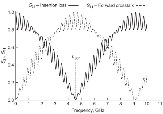
Figure 9-20 Modal decomposition of launch voltages when port 1 is driving as shown in Figure 9-15.
Reverse (Near–End) Crosstalk When the power is injected into port 1 and measured at port 3 for the circuit in Figure 9-15, it is called reverse crosstalk, as described in detail in Chapter 4. Reverse crosstalk is often referred to as near–end crosstalk. In terms of the scattering matrix, reverse crosstalk is defined as
To explain how reverse crosstalk behaves in the frequency domain, consider a transmission–line pair built in a homogeneous dielectric that is perfectly terminated with its characteristic impedance, so the forward crosstalk and reflections can be neglected. At dc, the crosstalk is zero because the coupling mechanism is dependent on Lm(∂i/∂t) and Cm(∂v/∂t) as described in Section 4.1. However, as the frequency starts to increase, energy will be coupled onto a victim line. As described in Section 9.1, the peak will occur when the imaginary part is zero as described by
(9-3b)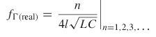
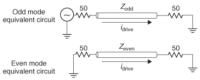
The peak value of the reverse crosstalk can be evaluated by decoupling the circuit into oddand even–mode equivalents and driving the system with a current idrive as shown in Figure 9-20. The voltages propagating in the odd and even modes are calculated with the modal impedances:
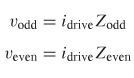
For the case where port 1 is driven and both odd and even modes are perfectly terminated,† the line voltages propagating on each line when the imaginary part
†This can be done with the appropriate T or pi termination network, as described by Hall [2000]. Another method is to choose the appropriate values of Zodd and Zeven, so the network is terminated. is zero are given by
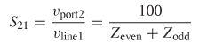
Since the voltage across the 50–Ω resistor at port 2 is υport2 = 50idrive, the insertion loss can be calculated:
and the peak value of the reverse crosstalk is the ratio of the voltage coupled onto line 2 and the voltage propagating on line 1:
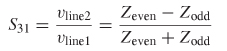
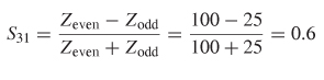
Example 9–6 Calculate the frequency where the insertion loss will be minimum and the reverse crosstalk will be maximum for a 10–in. loss–free homogeneous transmission line where εr = 4.0, with a circuit as shown in Figure 9-15. Assume that Zeven = 100 Ω Zodd = 25 Ωand all ports are terminated in 50 Ω
SOLUTION
Step 1: Calculate the propagation delay for the odd and even modes where 10 in. = 0.254 m and c = 3 x 10⁸ m/s:
Step 2: Use equation (9-3a) to calculate the frequency of the first hump in S31, where ![]()
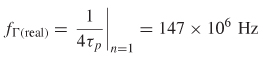
Step 3: Calculate the maximum value of the crosstalk:
Step 4: Calculate the minimum value of the insertion loss. Since this is a loss–free transmission line, the insertion loss (S21) will be minimum when the input reflections and crosstalk are maximum. Both the input reflections (S11) and the reverse crosstalk (S31) will peak when the frequency is equal to fΓ(real), as
Figure 9-21 Insertion loss and reverse crosstalk for Example 9–6.
described by equation (9-3b). Consequently, when S11 and S31 are maximum, S21 must be minimum and is calculated with equation (9-32a):
A simulation of this case is shown in Figure 9-21.
Relationship Between S– and Z–Parameters Perhaps the most intuitive form of network analysis are the Z–parameters, which were explained in Section 9.2.1. The disadvantage of using an impedance (or admittance) matrix is simply that they are impossible to measure directly at high frequencies. Fortunately, it is relatively easy to convert Z–parameters into S–parameters and vice versa. The derivation is shown here.
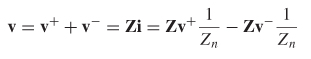
In matrix form, let’s begin with the voltage at port n of an N–port system, which is composed of an ingoing wave (v+ ) and an outgoing wave (v– ):
![]()
where the current is calculated from the port voltage and the port (reference) impedance Zn:
In matrix form this becomes
where Z is the impedance matrix. Assuming that the port impedance values are identical, equations (9–14) and (9–17) can be combined to show that the S–matrix can be calculated from v+ and v–:
Therefore, the scattering matrix can be calculated by solving (9–33) for (v– )(v+ )–1:
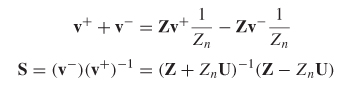
where U is the identity or unit matrix and Zn is the termination impedance of each port. The derivation assumes that each port is terminated in the same value. Equation (9-34) converts Z–parameters to S–parameters.
Solving (9–34) for Z allows the conversion from S–parameters to Z–parameters for an arbitrary–sized matrix:
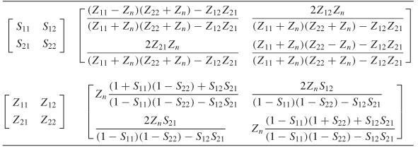
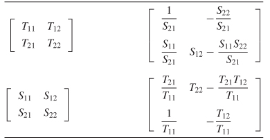
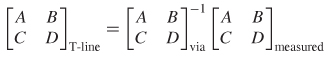
Equations (9–34) and (9–35) are solved for a two–port network and summarized in Table 9-1.
Impulse Response Section 8.1 we introduced the concept of an impulse response matrix to completely describe the behavior of a system. If the systems impulse
TABLE 9-1. Conversions Between S– and Z–Parameters for a Two–Port Network
matrix is known, it can be convolved with any arbitrary input (such as a pulse or a bit stream) and the signal integrity can be evaluated. It is impossible to measure the impulse response in the laboratory because it requires a driver capable of driving a Dirac delta function that has infinitely fast rise and fall times. Furthermore, even when a fast pulse is generated in the laboratory, inductance and capacitive loading of the probes introduces into the measured response unwanted noise, filtering, and resonances that are not associated with the electrical behavior of the device under test. Consequently, experimental evaluation of the impulse response in the laboratory using time–domain techniques is an impractical endeavor.
For most practical purposes, the impulse response of the system interconnects can be measured indirectly using a vector network analyzer (VNA), which is a device used to evaluate the scattering matrix as a function of frequency in the laboratory. Standard techniques to remove the parasitic inductance and capacitance effects of the probes and test fixtures from the measured scattering network are achieved through proper instrument calibration. Once the scattering matrix is measured, the impulse response can be calculated by taking the inverse Fourier transform, described in Section 8.1.4:
where S(ω) is the scattering matrix measured with a VNA.
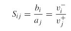
To calculate the impulse response, the scattering matrix must contain values for negative frequencies that obey the complex–conjugate rule to ensure a real–valued time–domain response, as described in Section 8.2.1. Since VNA measurements only provide values for the positive frequencies, the negative frequency values must be calculated from the positive values as
When calculating the impulse response using the fast Fourier transform (FFT), the negative values are appended to the end of the positive values, as demonstrated in Example 9–7.
Example 9–7 Calculate the impulse response from the measured values of S21 shown in Figure 9-22a.
SOLUTION
Step 1: Calculate the negative frequency values of S21 using (9–36b) as shown in Figure 9-22b.
![]()
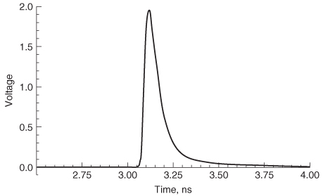
Step 2: Append the negative frequency values to the positive frequency values to create a continuous spectrum with both positive and negative frequencies. The magnitude of the continuous spectrum is shown in Figure 9-23a. Don’t get confused by the data format required by the FFT, which assumes that the input samples are periodic, resulting in a frequency response that looks more intuitive if proper windowing of the periodic response is chosen, as shown in Figure 9-23b.
Figure 9-22 For Example 9–7: (a) measured values of S21 for positive frequencies; (b) negative frequency values constructed from the complex conjugate of the positive frequencies.
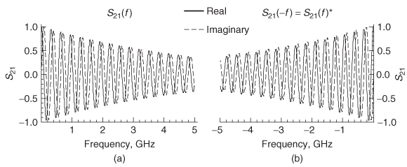
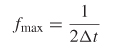
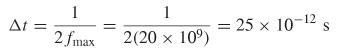
Step 3: Calculate the inverse FFT of the complex frequency spectrum to obtain the pulse response. In this case, the frequency data shown in Figure 9-22 were sampled at 100–MHz sample intervals for 1000 points for a bandwidth of 100 GHz. The final spectrum with the negative frequency values appended to the positive values has a total of 2000 sample points. Mathematica was used to perform the inverse FFT on the frequency data to produce the impulse response shown in Figure 9-24.
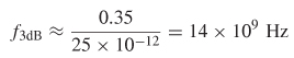
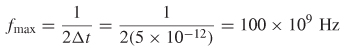
Although infinite bandwidth is required to produce a true impulse response with infinitely fast rise and fall times, the pulse response (i.e., single–bit response) as described in Section 8.1.5 can still be calculated with high accuracy if the harmonic bandwidth of the pulse is small compared to the bandwidth of the measurement. For example, if an 8–Gb/s single–bit response is calculated with rise and fall times of 35 ps, the bandwidth of the VNA used to evaluate the transfer function of the interconnects would need to be greater than 10 GHz, as calculated with Equation (8-8):
![]()
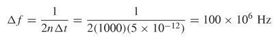
Furthermore, properties of the FFT place specific requirements on the frequencydomain bandwidth to generate minimum granularity in the time domain. If a minimum granularity of Δt is required for the time–domain waveform, the maximum
Figure 9-23 For Example 9–7: (a) magnitude of the frequency spectrum constructed by appending the measured positive frequency values of S 21 and the complex conjugate to create the negative frequency values; (b) FFT periodic treatment of the sampled data allows a more intuitive look at the magnitude of the frequency response when windowed properly.
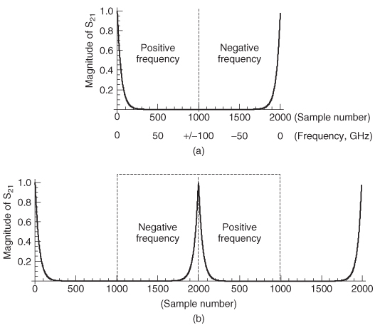
Figure 9-24 Impulse response calculated from the inverse FFT of the S 21 data shown in Figure 9-23.
positive frequency bandwidth of the measurement is defined by
To support a time–domain step size of Δt, the frequency sample size must be
and the maximum valid time–domain signal would be
where n is the number of samples for the positive frequency values.
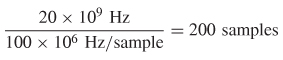
For example, if a time–domain granularity of 5 ps is required, the maximum bandwidth required using 1000 positive frequency sample points would be 100 GHz:
Consequently, a time–domain waveform constructed from a frequency–domain measurement requires significant bandwidth if fine granularity is required. Unfortunately, it becomes very difficult to perform VNA measurements above about 20 GHz. Both the calibration techniques and equipment costs become prohibitive.
Fortunately, there are mathematic ways to sidestep the lack of high–frequency measured data without losing time–domain granularity. As long as the spectral bandwidth of the digital waveforms propagating on the system interconnects are significantly lower than fmax extrapolation or zero padding of the measured scattering matrix can be used to increase granularity with only a small degradation in accuracy. For example, consider a driving digital waveform with rise and fall times of 25 ps. The spectral bandwidth of this waveform is approximated by equation (8-8):
Common bandwidths currently available on VNAs range from 20 to 110 GHz, which are equivalent to pulses with rise and fall times of about 3 to 18 ps.
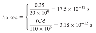
Therefore, measurements taken using a standard 20–GHz VNA would have adequate bandwidth to resolve rise and fall times as fast as 17.5 ps. Although a bandwidth of 20 GHz is sufficient to resolve the edge rate, the granularity of the time–domain waveform calculated using the FFT is only 25 ps, as calculated by (9–37a):
Consequently, extrapolation or zero padding is required to ensure reasonable granularity in the time–domain waveform, as demonstrated in Example 9–8.
Example 9–8 Assume that the complex values of S21 used in Example 9–7 have been measured to 20 GHz. Calculate the impulse response with a resolution of 5 ps.
SOLUTION
Step 1: Calculate fmax using equation (9-37a):
Step 2: Calculate the negative frequency values from –20 GHz to dc using equation (9-36b):
![]()
Step 3: Calculate the sample interval of the frequency–domain data assuming 1000 samples of the measurable positive frequency values:
Step 4: Calculate the number of zero points that need to be added to the spectrum. At a sample rate of 100 MHz, the number of samples up to 20 GHz is
Therefore, 800 zero points need to be added to both the positive and negative spectra to achieve ±100–GHz bandwidth.
Step 5: Append the positive and negative spectrums together as shown in Figure 9-25.
Step 6: Perform an inverse FFT on the zero–padded spectrum to get the impulse response, as shown in Figure 9-26.
Figure 9-25 Zero–padded spectrum. Bandwidh of measured response is 20 GHz and zero–padded to 100 GHz to ensure 5–ps resolution in the time domain.
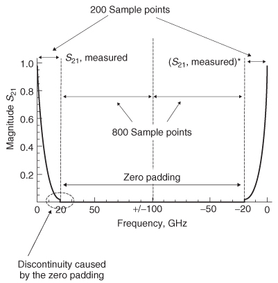
Figure 9-26 Impulse response calculated from the inverse FFT of the 20–GHz padded to 100–GHz S 21 data shown in Figure 9-25.
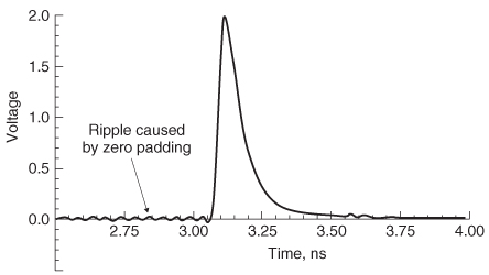
Note that the zero padding has introduced a small amount of ringing into the impulse response. The error is caused by the discontinuous spectrum where the measured data stops and the zero padding begins. This error can be minimized by increasing the bandwidth of the measured data, extrapolating the real and imaginary parts of the measured data instead of zero padding or smoothing the zero–padding discontinuity.
Figure 9-27 Two–port network used to describe ABCD parameters.
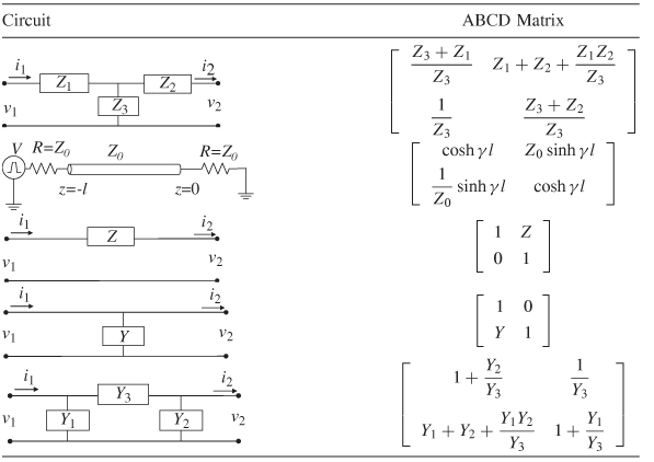
9.2.3 ABCD Parameters
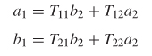
Consider the two–port network depicted in Figure 9-27. If the voltage and current are measured at the input and output ports, the system can be characterized in terms of its ABCD matrix. The ABCD parameters have several advantages over other network parameters. They allow the full description of a network in terms of input and output voltage and current, which makes them convenient for cascading circuits; they are easily related to equivalent circuits; and they provide a convenient basis for writing specialized programs that allow voltage and current sources to drive channels constructed from cascaded ABCD elements. Two–port ABCD parameters are developed here.
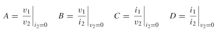
One significant difference between the ABCD matrix and the impedance matrix is the direction of i2, which is pointing out of, not into, port 2. This allows easy cascading of networks (which is addressed in Section 9.2.4). The ABCD values are evaluated as
Using the definition shown in equations (9–38), a set of linear equations can be written to describe the network:
which is more efficiently expressed in matrix form:
Consequently, if the ABCD matrix of a system is known, the response of the system can be predicted for any input.
Since the ABCD parameters are evaluated with short and open circuits as shown in equation (9–38), they are not practical to measure directly. However, relationships exist that allow the ABCD matrix to be calculated directly from the s–parameters as will be shown later.
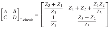
Figure 9-28 Deriving the ABCD parameters for a T–topology equivalent circuit.
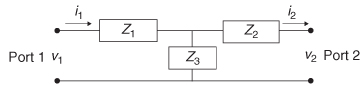
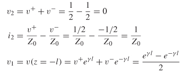
Relationship to Common Circuit Parameters The ABCD parameters can be used to create equivalent–circuit models for common circuit topologies. For example, consider the T–circuit shown in Figure 9-28. To determine A, port 2 must be open (since i2 = 0) while port 1 is driven with v1.
The term B is determined by shorting port 1 (since V2 = 0):
A current divider is used to calculate i2, which is substituted into the equation for B:
Since v1 /i1 is equal to the impedance looking into port 1, B can be simplified:
To determine C, port 2 must be open (since i2 = 0) while port i is driven with v1.
To determine D, port 2 must be short (since v2 = 0) while port 1 is driven:
Therefore, for a T–circuit like the one depicted in Figure 9-28, the ABCD matrix takes on the form
The ABCD parameters of a lossy transmission line can be derived for the case where the line is terminated is its characteristic impedance. This conversion is particularly useful for extracting transmission–line parameters such as Z0 and γ from measurements. For the case where the termination impedance is not equal to the characteristic impedance, the matrix can be renormalized as described in Section 9.2.6.
To begin the derivation, consider the transmission line in Figure 9-29:
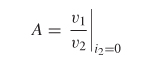
Figure 9-29 Deriving the ABCD parameters for a lossy transmission line.
Since i2 = 0, port 2 is open. Therefore, the voltage at port 2 will have an incident and a reflected component. For convenience, the total voltage at port 2 is set equal to 1:
The voltage at port 1 is calculated using equation (6-49) with z = –l.
The ratio of v1 and v2 is used to calculate A:
The term C is also calculated with i2 = 0.
The current i1 is calculated at z = –1 using the characteristics impedance.
The ratio of i1 and v2 is used to calculate C:
Terms B and D are calculated with v2 = o:
Since v2 = o, port 2 is shorted:
The ratio of v1 and i2 is used to calculate B:
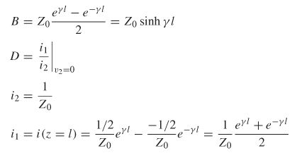
The ratio of i1 and i2 is used to calculate D:
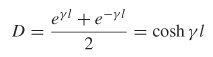
Therefore, the ABCD matrix for a lossy transmission line.
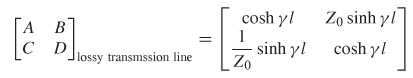
Using the same procedure, the ABCD parameters for a loss–free line can easily be derived where γ = jβ:
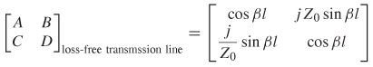
Table 9-2 depicts the relationship between common circuits and the ABCD parameters. These common forms are useful for extracting equivalent circuits from S–parameter measurements. Of course, a methodology is needed to convert S–parameters into an ABCD matrix, which is covered in the next section.
Relationship Between ABCD and S–Parameters To take advantage of the relationships between the ABCD matrix and common circuit forms, it is necessary to determine the relationship between the ABCD and S–parameters. The most straightforward derivation is first to define the transformation of ABCD parameters into a two–port Z–matrix and then use equation (9–34) to get the S–parameters.
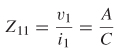
Beginning with the definition of Z11 from equation (9-8),
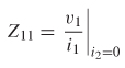
TABLE 9-2. Relationship Between Common Circuits and the ABCD Parameters
the ABCD equations reduce to

resulting in
The definition of Z12 is
so the ABCD equations reduce to
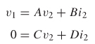
Solving the equations above for v1/i2 produces
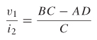
However, the convention for an ABCD matrix assumes that i2 is flowing out of port 2, and a Z matrix assumes that it is flowing into port 2. Consequently, the sign of i2 must be changed, which results in the definition of Z12 in terms of ABCD parameters:
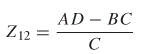
The terms Z21 and Z22 are derived using a similar procedure.

The final relationship between a two–port Z–matrix and the ABCD matrix is shown as
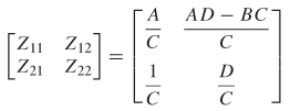
To derive the transformation of the ABCD to s–parameters, the results of (9–45) are substituted into equation (9-34). The final solution is summarized in (9–46), where Zn is the termination impedance at the ports, which are all assumed to be equal.
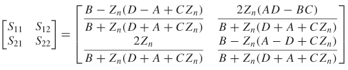
Similar techniques are used to derive the transformation of S into ABCD parameters. The complete sets of transformations are summarized in Table 9-3.
TABLE 9-3. Relationships Between Two–Port S and ABCD Parametersa
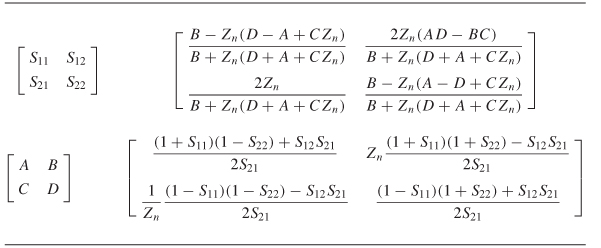
aZn is the termination impedance at the ports.
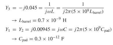
Figure 9-30 Via and equivalent circuit for Example 9–9.
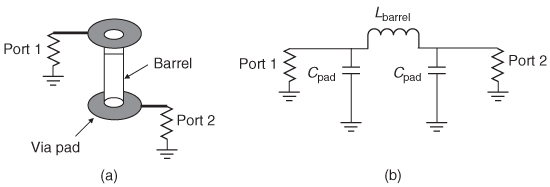
Example 9–9 Extract an equivalent circuit for the via shown in Figure 9-3oa from the following 5–parameter matrix measured at 5 GHz assuming port impedance values (Zn) of 50 Ω
SOLUTION
Step 1: Transform the 5–matrix into ABCD parameters using the relations in Table 9-3.
Step 2: Choose the form of the equivalent circuit. A signal propagating through the via will experience the capacitance of the via pad, the inductance of the barrel, and then the capacitance of the second pad. This configuration fits the pi model in Table 9-2 as shown in Figure 9-30b.
Step 3: Use the relations in Table 9-2 to calculate the admittance of each segment in the pi model:
Due to symmetry in the circuit, Y1 = Y2.
Step 4: Calculate the circuit values:
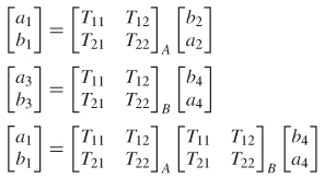
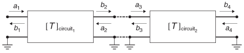
9.2.4 Cascading S–Parameters
One of the most useful aspects of network analysis is the ability to cascade independently measured structures. For example, if the S–parameters are measured independently for a transmission line, via, package, and connector, the engineer has the ability to create the response of an entire channel from the individual measurements. This allows S–parameter files to be used as portable models, gives the designer the ability to evaluate different topologies, and provides the mechanism to deembed or calibrate out unwanted items in the measurements. The two most common methods of cascading S–parameters are with the ABCD parameters and the T–matrix.
Cascading with the ABCD Matrix For two–port networks, the most common cascading methodology is to use the ABCD parameters. Cascading is achieved simply by multiplying the ABCD matrices. This is possible because of the current convention that flows outward at port 2, as shown in Figure 9-27. For example, consider the ABDC parameters of the two cascaded circuits shown in Figure 9-31. The equations that describe the port voltage and currents of circuits 1 and 2 can
Figure 9-31 ABCD parameters are cascaded though multiplication.
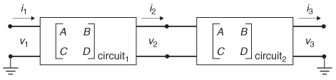
easily be written.
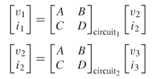
Note that the output of circuit i is v2 and i2, which is the input of circuit 2. This allows the simple substitution of
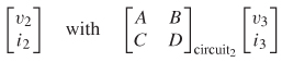
resulting in
Therefore, two–port S–parameters can be cascaded by converting to ABCD parameters and multiplying. The cascaded scattering matrix is then calculated by converting the cascaded ABCD matrix back to S–parameters using Table 9-3. The procedure is demonstrated in Example 9–i0.
Example 9–10 Using the two independently measured values of S–parameters for a via and a loss–free transmission line at 5 GHz, calculate the, equivalent S–parameters that would be measured if the two circuits were cascaded as shown Figure 9-32. Assume that the termination impedance is 50 Ω
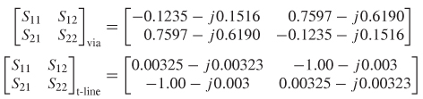
Figure 9-32 For Example 9–10: (a) configuration of the independently measured via; (b) transmission line; (c) via cascaded with the transmission line.
SOLUTION
Step 1: Convert to ABCD parameters using Table 9-3:
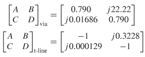
Step 2: Multiply the ABCD matrices:
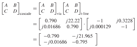
Step 3: Convert ![]() back to s–parameters using Table 9-3 where
Zn = 50 Ω (the termination impedance)
back to s–parameters using Table 9-3 where
Zn = 50 Ω (the termination impedance)
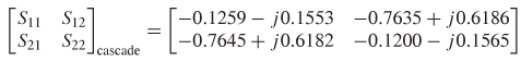
The cascaded S–matrix is equivalent to what would be measured if the via was cascaded with the transmission line, as shown in Figure 9-32c.
Cascading with the T–Matrix Another method commonly used to cascade S–parameters is the T–matrix, sometimes called transmission parameters. The T –parameters are derived simply by rearranging the equations for the S–parameters. Equation (9–18) describes the relationship between the incident power waves a and the exiting power waves b:
To facilitate the cascading of networks by simple matrix multiplication, the equation needs to be rearranged so that the ingoing and outgoing waves of port 1 can be described in terms of the waves at port 2. This is done with the T–matrix. A two–port T –matrix is
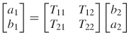
If the output of circuit A is attached to the input of circuit B, the total response can be calculated simply by multiplying the T–matrices, because the power wave exiting circuit A is b2, which feeds into the input of circuit B, which is a3. Therefore, b2 = a3 and a2 = b3, as shown in Figure 9-33.
Therefore, S–parameters can be cascaded by converting to T–parameters and multiplying. The cascaded scattering matrix is then calculated by converting the product of the T–matrices back to S–parameters.
Conversion between the T and S–parameters (and vice–versa) requires simple algebraic manipulation of the equations, which can be done for any number of
Figure 9-33 T–parameters are cascaded through multiplication.
ports. The conversion from S– to T–parameters is derived here for a two–port system to demonstrate the process. To begin, the equations that relate the incoming power waves to the outgoing are written
and equation (9-47) is expressed in algebraic form:
From the equations above, the individual T –parameters can be defined in terms of the S–parameters:
TABLE 9-4. Relationships Between T and S–Parameters for Two–Ports
A very similar analysis is used to transform the T–parameters back into S–parameters, which is left to an exercise for the reader. The transformations for two ports are summarized in Table 9-4.
The four–port T –matrix takes the form
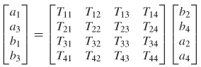
for the network shown in Figure 9-34. The transformations between T– and S–parameters for n–ports is developed in an identical manner, which is shown in Appendix B.
9.2.5 Calibration and De–embedding
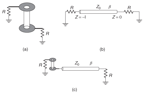
Very often in digital design it is desirable to measure a component such as a transmission line, a CPU socket, or a daughter–card connector using a vector network analyzer (VNA). The measurement can be used to create an equivalent–circuit model, validate the modeling methodologies used to simulate the channel, or estimate the performance of a component. Practicality dictates that the device under test (DUT) is usually mounted in a fixture and connected to the VNA with a cable using probes or SMA connectors. Consequently, methodologies are needed to separate the s–parameters of the DUT from the test fixture, cables, or probes. In this section we introduce the basic calibration and deembedding methodologies so that the concept will be understood. Since each measurement setup requires a specialized calibration and deembedding procedure, the breadth of the topic is too wide to be covered here.
Figure 9-34 Four–port network.
The terms calibration and deembedding refer to the same concept: remstepoving an unwanted part of the measurement. More specifically, calibration refers to removing the effect of the VNA cables and probes, and deembedding refers to removing unwanted portions of the DUT, such as a via, a test fixture, or a cable connector. A VNA measures S–parameters as ratios of complex voltage amplitudes. The reference for the measurement is some place within the VNA, not at the cable ends which are attached to the DUT, so the measurement will include the losses and phase delays of the cables, connectors, and probes used to connect the DUT to the analyzer. Calibration refers to the removal of these unwanted effects from the measured response so that only the measured response of the DUT remains. Figure 9-35 demonstrates this concept.
For calibration purposes, it is convenient to work with ABCD parameters. For example, the measurement setup in Figure 9-35 can be represented by cascaded ABCD matrices:
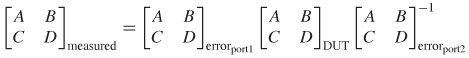
Note that the ABCD matrix for port 2 is inverted because the VNA drives into the port and measures the responses at all other ports. The inversion simply ensures that it represents current flowing from port 2 into the DUT and not the other way around. Equation (9-50) suggests that if the ABCD matrices of the errors are known, the ABCD matrix (and thus the S–parameters) of the DUT can be calculated. In short, the calibrated measurement is simply the error–corrected S–parameters.
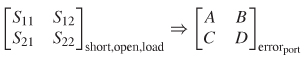
The most straightforward method to remove the errors and calibrate a VNA is to use three or more carefully controlled loads, such as a short, open, and
Figure 9-35 Calibration removes the unwanted parts of the measurement, such as the cable and probe effects.
Figure 9-36 The simplest way to calibrate a VNA is to characterize the port error by driving different loads (ZL): an open, a short, and a resistive load.
precision resistive load. For example, consider Figure 9-36, which represents one port of a VNA driving a load ZL . The equations for the S–parameters can be written in terms of the reflection coefficient at the load where the incoming wave at port 2 (a2) is simply the reflected portion of the exiting wave (b2) a2 = b2ΓL.
The input reflection Γin is the ratio of the reflected wave b1 to the incident wave a1:
If it is assumed that the error term is reciprocal, S21 = S12, the input reflection equation can be simplified:
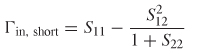
To calibrate the effect of the errors out of the measurement, the S–parameters must be found. This is done by considering three known values for the load, ZL: a short, an open, and a perfectly matched resistor. When the load is shorted, the reflection at the load is ΓL = –1, which reduces (9–52) to
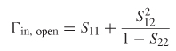
When the load is open and perfectly impedance matched, the reflection at the load is ΓL = 1 and ΓL = 0 respectively, producing
By measuring the open, short and matched loads, the three equations above can be solved simultaneously for S11, S12, and S22:
The equations above are then used to create a scattering matrix for the errors at the ports:
Finally, the measurements of the DUT are calculated by multiplying by the inverse of the error terms:
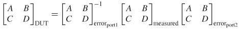
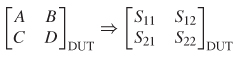
The calibrated S–parameters are obtained by converting the ABCD matrix of the DUT calculated with (9–56) using Table 9-3.
Basic deembedding principles utilize the same concepts to remove unwanted parts of the measurement. For example, Figure 9-32c shows a case where a via is cascaded with a transmission line. If it is desired to obtain only the measurements of the transmission line, the effects of the via must be deembedded. If the test board contains suitable structures to measure the S–parameters of the via in isolation, it can be effectively deembedded from the measurements using the same procedure shown in (9–56):
Using the concept of cascaded matrices, any number of structures can be deembedded from the measured data as long as the S–parameters for the structures are known.
9.2.6 Changing the Reference Impedance
S–parameters are dependent on the reference impedance of the VNA. If the port impedance values change, the S–parameters change. It is generally standard to measure S–parameters assuming a reference impedance of 50 Ω at each port. However, sometimes the port impedance values need to be adjusted after the measurements are performed. For example, perhaps the port impedance of the VNA was determined to be something other than 50 or the engineer wished to examine the performance of the circuit referenced to an impedance consistent with the transmission lines used in a specific board design. When an S–parameter is measured with a reference impedance at the ports of Zn, it is said to be normalized to that impedance.
To renormalize the S–matrix from Zn1 to Zn2, the definition of the Z–parameters from equation (9-35) is used:![]() (9-35)
(9-35)
Since the impedance matrix is not dependent on the port impedance, it can be used to renormalize the S–matrix.
![]()
Solving for S2 yields
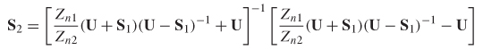
Example 9–11 Renormalize the following S–matrix measured with a 50–Ω reference load to 75 Ω
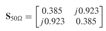
SOLUTION Using equation (9-59), the S–matrix can be manipulated so that it looks like it was measured with a 75–Ω reference impedance.
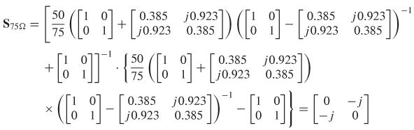
Therefore, the magnitude of the renormalized S–matrix is
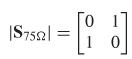
meaning that the transmission line is loss free with a characteristic impedance of 75 Ω since there is no reflection (S11 = 0) and the insertion loss is unity (S21 = 1).
9.2.7 Multimode S–Parameters
In Chapter 4 differential signaling was explained. Since many of the high–speed buses being designed in modern computing systems consist of differential pairs, it is often convenient to describe the behavior of the interconnects in terms of multimode S–parameters. The multimode S–matrix breaks the signal on a differential pair into terms of differential (i.e., odd mode) and common (i.e., even mode) signaling states. A multimode matrix for two modes can be derived
Figure 9-37 A pair of coupled transmission lines is a common example of a four–port network that is conveniently described with a multimode S –matrix.
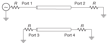
directly from the four–port S–parameters. For example, the S–parameters of the four–port system pictured in Figure 9-34 are shown as follows:
An example of a four–port system is two coupled transmission lines, as shown in Figure 9-37. To derive the multimode matrix, it is first necessary to calculate the S–parameters for each mode.
The differential S–parameters, where the energy is being transmitted in the odd mode, are calculated by driving the four–port network with +v on port 1 and –v on port 3 when ports 2 and 4 are not being driven. This allows (9–60) to be simplified.
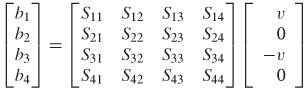
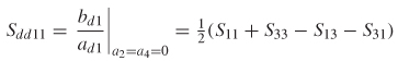
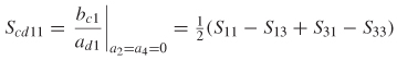
The differential return loss at port i can then be calculated algebraically where bd1 = b1 – b3 and ad1 = a1 – a3 = v – (–v) = 2v.
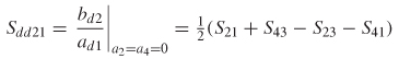
Sdd11is a measure of the differential energy reflected, or returned to the source. Similarly, the differential insertion loss is calculated wherebd2 = b2 – b4 and ad1 = a1 – a3 = v – (–v) = 2v.
Sdd21 is a measure of the differential energy transmitted across the network from port 1 to port 2.
Identical analysis can be used to calculate the common–mode S–parameters, where the energy is being transmitted in the even mode, by driving the four–port network with +v on port 1 and +v on port 3 when ports 2 and 4 are not being driven. This allows (9–60) to be simplified wherebc1 = b1 + b3, bc2 = b2 + b4, and ac1 = a1 + a3 = v + v = 2v.
The common–mode S–parameters are easily obtained algebraically from (9–63):
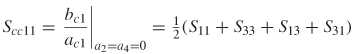
Equations (9–64a) and (9–64b) describe how much energy is being reflected and transmitted when the four–port system is being driven with a common–mode source (i.e., the system is being driven in the even mode).
As described in Chapter 4, for a system with two signal conductors, the voltages at the ports are combinations of odd and even modes. Consequently, for a perfectly symmetric system (where each leg of the differential pair is electrically identical), if the system is driven differentially, all the energy will be contained within the odd mode. However, if the pair exhibits any asymmetry, a portion of the energy will be flowing in the even mode. The multimode matrix also accounts for the differential–to–common mode conversion, which describes the amount of energy being transformed into the even mode when the system is being driven differentially and the common mode–to–differential conversion, which tells how much energy is being converted to the odd mode when driven commonly. Since most high–speed buses are driven differentially, the differential–to–common mode conversion is the most important parameter of the two.
The differential–to–common mode S–parameters, where the energy is being transmitted in the odd mode and received in the even mode, are calculated by driving the four–port network differentially at the driver and sensing in common mode at the receiver. The differential–to–common mode coefficients are bc1 = b1 + b3, bc2 = b2 + b4, and ad1 = a1 – a3 = v – (–v) = 2v.
The common mode–to–differential S–parameters, where the energy is being transmitted in the even mode and received in the odd mode, are calculated by driving the four–port network in the common mode and sensing differentially at the receiver. The derivation is left to the reader.
The multimode S–parameters for a four–port system can be combined to create the multimode matrix
Note that each quadrant of the multimode matrix represents unique parameters. For example, the upper left quadrant is the differential S–parameter matrix,
which assumes that all the energy is sourced and sensed in a differential manner. Consequently, the multimode matrix takes the form
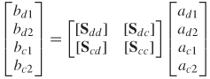
where each matrix describes a specific driving and receiving configuration:
Sdd: Driver and receiver are differential.
Scc: Driver and receiver are common mode.
Sdc: Driver is common mode and receiver is differential.
Scd: Driver is differential mode and receiver is common mode.
The format of (9–67c) allows the four–port S–parameters to be reduced to an equivalent simple two–port system for specific circumstances. For example, in high–speed differential buses, each pair is driven and received assuming that all
Figure 9-38 Unbalanced differential pairs cause energy to be converted from the odd mode to the even mode, which looks like additional differential insertion loss.
energy is in the odd mode, which means that for all practical purposes, equation (9-67b) is sufficient for design purposes.
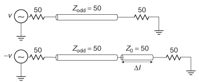
Invariably, a question is asked: If there is significant energy in the even mode, doesn’t the common mode matrix need to be accounted for? The answer is that it is already included in the differential matrix of (9–67b). If an asymmetrical four–port system is driven differentially, the energy that is converted to common mode will simply look like differential insertion loss. For example, consider the loss–free unbalanced differential transmission line pair being driven in the odd mode in Figure 9-38. Since the system is being driven differentially (in the odd mode), and the odd–mode impedance is equal to the termination, there will be no reflections. However, since it is unbalanced, it is expected that a portion of the energy will be transferred to the even mode. From a differential receiver’s point of view, this will look like extra channel loss.
To demonstrate this concept, consider the case where the difference in length between the legs of the differential pair (Δl) is 200 mils with a delay of 27.77 ps (refer to Figure 9-38). If the initial phase difference between v + and v– at the driver is of 180°, when the signals arrive at the receiver, the phase difference will no longer be equal to 180°, due to the extra length on the second leg. The actual phase difference at the receiver can be calculated using equation (9-22) as a function of frequency. For example, at 1 GHz the phase difference at the receiver will be
![]()
meaning that since the signals are no longer exactly 180° out of phase, and some of the energy is being dumped into the even mode.
As the frequency increases, the phase difference due to the extra delay will approach 180°. When θ = 180°, the differential signal at the driver has been fully transformed into a common–mode signal at the receiver. When the delay difference between the legs of the differential pair is 27.77 ps, the frequency where the signal is 100% common mode at the receiver is 18 GHz:
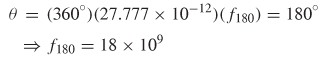
Figure 9-39 As the frequency increases, small asymmetries in a differential pair will cause larger phase differences between signals propagating on each leg, causing energy to be converted from odd to even mode. This shows up as differential insertion loss. In this case the differential signal is 100% converted to common mode at 18 GHz.
So at 18 GHz, the phase difference at the receiver will be
![]()
Therefore, at 18 GHz the differential insertion loss is zero because there is no longer any differential energy being transmitted to the receiver because all the energy has been converted to the common mode.
Figure 9-39 shows the S–parameters for the loss–free perfectly terminated asymmetrical transmission line with a interleg delay difference of 27.77 ps. Note that the differential energy transferred from port 1 to port 2 (Sdd21) decreases until 18 GHz, after which it begins to increase again. At 1 GHz (where θ = 190°), Scd21 = 0.1, which means that 10% of the differential energy is lost to the common mode. At 18 GHz, Scd21 = 1.0, so 100% of the energy is lost to the common mode. It is easy to see that the decrease in Sdd21 corresponds with the increase in Scd21 .
Do not falsely conclude that differential signals can be transmitted properly at frequencies above f180 (18 GHz in this example). Although Sdd21 increases, the phase difference between signals on each leg approaches 540° (3 . 180°), not the ideal value of 180°. For a digital signal, this means that the bit on line 1 is 180° out of phase with the next bit in the digital pulse train on line 2. Therefore, even though the common–mode conversion is small, the data are invalid.
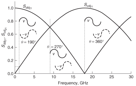
When loss is included in the transmission line, the Scd21 curve will peak at a lower frequency that does not correspond to the point where the differential–tocommon mode conversion is 100%, as shown in Figure 9-40. Be careful not to misinterpret the differential S–parameter data. The mode conversion is 100% when Sdd21 is zero, not necessarily when Scd21 is maximum.
Figure 9-40 For a loss–free case, the differential–to–common mode conversion curve will be maximum when the phase difference between legs is 180°. However, for a lossy case, the S cd21 curve will peak at a lower frequency, due to losses from the conductors and dielectrics.
9.3 PROPERTIES OF PHYSICAL –PARAMETERS
S–parameters are a valuable tool in digital design. They can be used to analyze the performance of a component, extract equivalent–circuit models, or be employed as a tool–independent portable model. The problem arises that S–parameters are difficult to generate accurately. For example, proper calibration of a vector network analyzer to high frequencies is both a science and an art. If probe effects are not removed or test fixtures are deembedded improperly, the S–parameters could contain significant errors that are difficult to detect. Additionally, when component models (i.e., for a connector or CPU socket) are distributed to engineers in the form of a frequency–dependentS–parameter file, the assumptions of how the model was constructed are lost, so it is impossible to judge correctness or applicability. Fortunately, even though it is impossible to judge the accuracy of S–parameters without comparison to measurements or examination of the underlying model, the concepts outlined in Chapter 8 can be used to look for gross errors that blatantly violate the laws of physics.
9.3.1 Passivity
As defined in Section 8.2.2, a physical system is passive when it is unable to generate energy. For digital design, S–parameters are used to analyze the physical components of the bus, such as the transmission lines, sockets, and connectors, none of which generate energy. Therefore, in digital design, if an S–parameter measurement or model is shown to be nonpassive, either the VNA was not calibrated correctly or the underlying assumptions of the modeling methodology are wrong. A practical test for the passivity of S–parameters can be developed directly from equations (8–22) and (8–23)[Ling, 2007].
Since power must be conserved, the power absorbed by the network (Pa) is equal to the power driven into the network less power flowing out:
where Pa ≥ 0 for a passive network. If Pa < 0, the network is generating power and the system would be considered nonpassive. This allows equation (8–22) to be written in terms of the power wave matrices that will produce a real value for the power absorbed by the network. A system is passive if
where a is a matrix that contains all the power waves incident to each port, b contains the power waves coming out of each port, and xH indicates the conjugate transpose (sometimes called the Hermitian transpose), which is calculated by taking the transpose of x and then taking the complex conjugate of each entry.
Using the definition of S–parameters from equation (9-18), the passivity requirement of (8–23) can be rewritten as
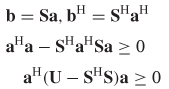
where U is the unity (identity) matrix. Equation (9-68) leads to the general requirement for passivity:
If SHS is greater than 1, the requirement of (8–22) is violated and the system is not passive.
A quick test to ensure passivity can be derived based on the eigenvalues of SHS. The eigenvectors ζ and eigenvalues λ are determined from the solution of the equation
![]()
Techniques for calculating the eigenvectors and eigenvalues are detailed by O’Neil [1991]; however, there are many software packages that can be used, such as Mathematica or Matlab.
The eigenvectors can be formed into an N x N matrix,
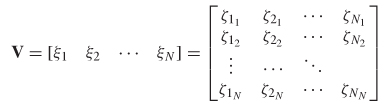
with the property that VVT U. The matrix SHS can be diagonalized into its eigenvalues with
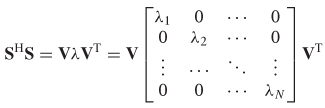
The definitions above allow (9–68) to be rewritten in terms of the eigenvalues:
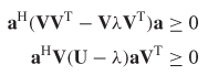
Equation (9-71) leads to a simple test for passivity [Ling, 2007]. Since U – λ must be greater or equal to zero and nonnegative, the system is passive if all the eigenvalues are between 0 and 1. The test for passivity is shown as
Some tools employ the strategy of applying correction algorithms for the nonpassive cases. Generally, the use of a passivity–corrected model or measurement is an unwise strategy because nonpassivity indicates an incorrect model or calibration. The best strategy is to reevaluate the method for equating the S–parameters and fix the problem.
9.3.2 Reality
Time–domain signals that are used to analyze digital interconnect are real. In other words, there is no imaginary part of a time–domain signal that can exist in nature. As mentioned in Section 8.2.1, the mathematical requirement for a frequency–domain response to ensure a real time–domain waveform is
where* indicates the complex conjugate and j and i represent the driving and receiving ports of the S–parameters. Most S–parameter data are presented only with positive frequency–domain data, and the tools construct the negative frequency portion from (9–73). However, if the negative frequency values of the S–parameters are available, (9–73) is a useful check.
9.3.3 Causality
As covered in Section 8.2.1, one seemingly obvious requirement of a model or measurement is that its output cannot precede its input. In other words, an effect cannot precede its cause. This fundamental principle is called causality . Very often, VNA calibration problems or incorrect model assumptions generate S–parameters that are not causal. This error becomes especially critical when S–parameters are used to represent the behavior of physical channel components when simulating system performance. Causality errors will introduce delay and amplitude errors in the time–domain responses, as well as distort waveforms to such a degree that signal integrity may be falsely predicted, which can lead to false solution spaces, incorrect equalization settings, and incorrect understanding of bus performance. Many commercially available tools create models that are noncausal simply because of the assumptions of a frequency–invariant dielectric model where er and tan 8 are not properly related. Figure 8.14 is a good example of how a noncausal model can distort the waveform of a single bit. The errors depicted in Figure 8.14 will be amplified for very long channel lengths and high frequencies. Many of the digital designs created in the past were designed using noncausal models that assume frequency–invariant dielectric parameters. At low data rates (below about 1 to 2 Gbit/s) and short lengths (a few inches), causality errors do not appreciable affect signal integrity. However, at high frequencies and/or long lengths, they can completely destroy the model’s ability to predict realistic behavior.
Causality requirements are often difficult to judge by looking directly at S–parameters because the phase errors are small compared to the propagation delay of the structure. Furthermore, even if the causality errors of a single component such as a connector or via are small in isolation, when numerous models are cascaded in a complete channel simulation the errors become cumulative. Consequently, it is important to check the causality of each component as well as the system response for the entire channel.
As described fully in Section 8.2.1 and demonstrated in Examples 8–3 and 8–4, causality can be tested by performing the Hilbert transform of the real part and ensuring that it is identical to the imaginary part. If it is not identical, the model is not causal. However, care should to be taken when performing this test because for bandlimited data, the Hilbert transform can exhibit truncation errors.
Equation (8-19) is adapted to calculate the Hilbert transform of the real part of the S–parameter data,
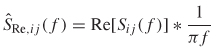
where ŜRe,ij(f) denotes the Hilbert transform of the real portion of the S–parameter, Sij(f) is an S–parameter where port j is driving and port i is receiving, and * denotes convolution. The S–parameter is causal when (9–75) is satisfied:
To implement (9–74), it is often necessary to reconstruct the negative frequency components of the response using
Figure 9-41 Classic impulse response behavior of a severely noncausal S –parameter. Note the precursor error, where part of the energy is arriving too early.
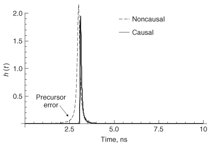
The most straightforward way to calculate the Hilbert transform is to use the Fourier transform (usually in the form of the fast Fourier transform), as demonstrated in Examples 8–3 and 8–4.
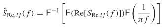
If the fast Fourier transform is used, the negative frequency values must be appended to the end of the positive values, as demonstrated in Example 9–7. A less rigorous way to evaluate the causality is to transform the S–parameters into an impulse response, as described in 9.2.2. If there is no distinct point at which the pulse arrives, it is an indication of a noncausal response, as shown in Figure 9-41.
9.3.4 Subjective Examination of S–Parameters
Often, it is desirable to recognize the trustworthiness of S–parameter data without the rigor of the mathematical analysis above. Understanding the basic properties of S–parameter data will allow an intuitive analysis. For example, a gross passivity violation can often be seen by observing the magnitude of the insertion loss. Figure 9-42 shows an example of measured insertion loss for a transmission line. Note that the scale often used with VNA measurements is, in decibels,
where mag is the magnitude of the complex S–parameter value. Notice how S21 in Figure 9-42 rises above zero at the lower frequencies, indicating that the transmission line has gain and is therefore producing energy and nonpassive
Figure 9-42 Bad S–parameter measurement of a transmission line, showing passivity violations due to incorrect VNA calibration.
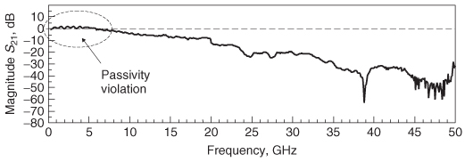
Figure 9-43 Bad S–parameter measurement of a transmission line, showing passivity violations at high frequencies where the VNA calibration breaks down.
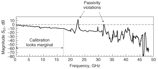
(0 dB is equal to an insertion loss of 1 on a linear scale). In this case, the passivity violation was a result and an incorrect calibration of the vector network analyzer. Another example of a severe passivity violation is shown in Figure 9-43, where the calibration breaks down after about 17 GHz. Even below 17 GHz this measurement looks questionable, due to the significant amount of nonperiodic ripples on the waveform. Periodic ripples would probably be a result of reflections or crosstalk, but nonperiodic noise on S21 indicates an inaccurate measurement.
Figure 9-44 shows an example of a good measurement of a 5–in. microstrip transmission line on a FR4 substrate. Note that the insertion loss does not rise above 0 dB and that it does not contain any nonperiodic noise. It should be noted that the S–parameters could still be nonpassive even if S21 does not rise above 0 dB. Passivity can only be verified using the techniques outlined in Section 9.3.1; however, simple observation of S21 is often sufficient to catch gross errors.
The periodic behavior of S11 can also be used to get an intuitive feeling about the validity of the S–parameters by ensuring reasonable phase delays. If the structure under test is a transmission line, the return loss (S11) should be periodic and the distance between peaks (or dips) is related to the time delay with equation (9-4). The propagation delay can be double–checked at various frequencies. From Figure 9-44 the propagation delays are calculated:
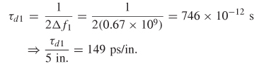
Figure 9-44 Good S–parameter measurement with no obvious problems.
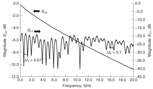
Figure 9-45 Good S–parameter measurement with no obvious problems, showing the proper relationship between the real and imaginary parts.
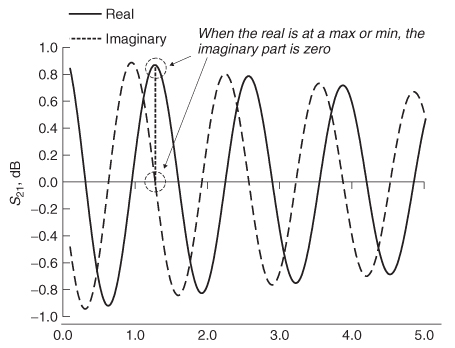
Since the delay of a typical microstrip line on FR4 is about 140 to 160 ps/in., the result seems reasonable.
At higher frequencies, the same test can be applied. From Figure 9-44, Δf2 = 0.7 GHz.
Note that the delay is less that it was at the lower–frequency test. This confirms the validity of the measurement because the dielectric constant, and therefore the propagation delay, should decrease with frequency, as described in Chapter 6.
Finally, the relationships between the real and imaginary parts of S21 can be examined. Figure 9-45 shows the real and imaginary parts of the insertion loss for the 5–in. transmission line measured in Figure 9-44. As discussed in Section 9.1.1, when the real part peaks, the imaginary part should be zero.
REFERENCES
Ling, Yun, 2007, Demystify S–parameters, I: The basics, class given at Intel Corporation. O’Neil, Peter V., 1991, Advanced Engineering Mathematics, Wadsworth, Belmont, CA.
Hall, Stephen, Garrett Hall, and James McCall, 2000, High Speed Digital System Design, Wiley–Interscience, New York.
PROBLEMS
9–1 Consider the measured S–parameters of a transmission line shown in Figure 9-46. What is the propagation delay of the transmission line? What is the characteristic impedance of the transmission line assuming that the port impedances are 50 Is the measurement valid? How can you tell?
9–2 Consider the S–parameters shown in Figure 9-47 of a transmission line. Are these S–parameters valid? How can you tell?
9–3 Consider the measured S–parameters of a transmission line shown in Figure 9-48. Are these S–parameters valid? How can you tell?
9–4 Derive the conversion from T–parameters back into S–parameters for two ports.
9–5 Derive the formulas to extract R, L, C, and G from a transmission line with arbitrary impedance. Prove that the method is accurate by extracting the frequency–dependent R, L, C, and G from a simulated transmission line.
9–6 Calculate the common–mode matrix and the common mode–to–differential conversion matrix of a four–port S–matrix.
Figure 9-46 Figure for Problem 9–1.
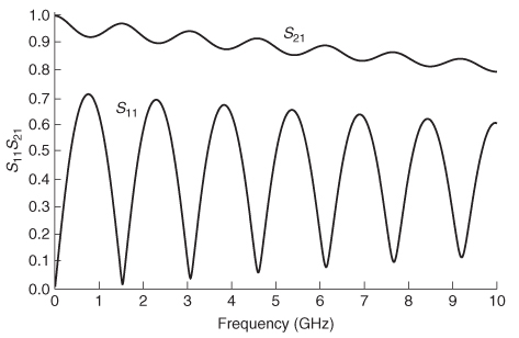
Figure 9-47 Figure for Problem 9–2.
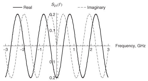
9–7 If a differential pair has 10% of its energy transformed into the common mode when driven differentially, is 10% of its energy transformed into the differential mode when driven commonly? Show the math to support your answer.
9–8 Derive the ABCD matrix for the pi circuit shown in the bottom of Table 9-2.
9–9 For the differential pair in Figure 9-49, at what frequency will the ACCM be 100%? Assume that the effective permittivities are erodd = 3.5 and er = 4.0.
Figure 9-48 Figure for Problem 9–3.
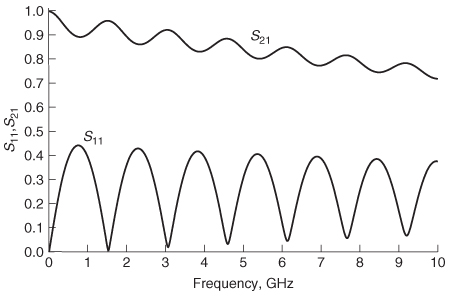
Figure 9-49 Figure for Problem 9–9.
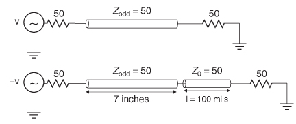
9–10 Derive the equations to renormalize the S–matrix measured with 50– Ω loads at each port to arbitrary and different reference impedances at each port.
9–11 Derive the two–port S–parameters for a frequency–dependent, causal 10–in. transmission line from 10 Hz to 100 GHz. Using a tool such as Mathematica or Matlab, plot the S–parameters and prove that they are passive and causal.
9–12 From the S–parameters calculated from the transmission line in Problem 9–11, calculate the pulse (single–bit) response for a 15–Gbit/s data rate.
9–13 Create the S–matrices for 4and 10–in. transmission lines using the method derived in Problem 9–11. Cascade the S–parameters to get the equivalent S–matrix for a 14–in. transmission line. Compare the cascaded S–matrix to that of a single 14–in. transmission line.
† The terms insertion loss and return loss should not be confused with ohmic or radiation losses. When a system is said to be loss free, it means that the power lost through heat, such as conductor and dielectric losses, does not exist. It also means that no energy is being lost through radiation into free space.