
5
NONIDEAL CONDUCTOR MODELS
5.1 Signals Propagating in Unbounded Conductive Media
5.1.1 Propagation Constant for Conductive Media
5.1.2 Skin Depth
5.2 Classic Conductor Model for Transmission Lines
5.2.1 DC Losses in Conductors
5.2.2 Frequency-Dependent Resistance in Conductors
5.2.3 Frequency-Dependent Inductance
5.2.4 Power Loss in a Smooth Conductor
5.3 Surface Roughness
5.3.1 Hammerstad Model
5.3.2 Hemispherical Model
5.3.3 Huray Model
5.3.4 Conclusions
5.4 Transmission-Line Parameters for Nonideal Conductors
5.4.1 Equivalent Circuit, Impedance, and Propagation Constant
5.4.2 Telegrapher’s Equations for a Real Conductor and a Perfect Dielectric
References
Problems
As digital systems evolve and technology pushes for smaller and faster designs, the geometric dimensions of the physical platform are shrinking. Smaller dimensions and higher data transmission rates necessitate the use of proper techniques to model both the frequency dependent resistive losses and inductance. Without proper models that accurately predict these quantities, simulation-based bus design for multigigabit data rates is not possible. Frequency-dependent resistive losses, for example, will affect bus performance by decreasing the signal amplitude and slowing edge rates, which in turn affects voltage and timing margins, respectively. In addition, frequency dependent inductance models are required to preserve causality , which is discussed in Chapter 8 and Appendix E. In prior days it was possible to utilize simpler conductor models for digital designs because bandwidth demands were much lower. However, as digital data rates increase, the assumptions and approximations of traditional conductorsgin to break down. Consequently, the signal integrity engineer is now required to learn new techniques that compensate for variables that were insignificant in past designs.
So far in this book we have covered the topics of electromagnetic theory for signal integrity engineers, transmission-line fundamentals, and crosstalk. Up to this point, the conductors were assumed to be infinitely conductive and the dielectric was assumed to be a perfect insulator. In this chapter we develop modeling techniques to predict properly the electrical behavior of conductors used to design transmission lines on printed circuit boards, multichip modules, and chip packages. First, classic electromagnetic theory will be used to derive the frequency dependence of resistance and inductance for smooth conductors with finite conductivity. Next, three different methodologies for modeling the effects of rough copper on the electrical parameters of the transmission lines will be introduced. Detailed analysis of how currents flow on a rough surface will give physical insights into the mechanisms of surface roughness losses. Finally, a new circuit model for a transmission line that accounts for realistic conductors will be introduced along with a modified version of the telegrapher’s equations that account for realistic conductor losses.
5.1 SIGNALS PROPAGATING IN UNBOUNDED CONDUCTIVE MEDIA
The topic of uniform plane waves propagating in a lossless media was discussed in Section 2.3, where the influences of the material properties µ and ε were observed. In Chapter 3 we described how the waves propagated when confined to the physical dimensions of a transmission line, yet the problem was still idealized because it was assumed that the dielectric was a perfect insulator and the conductor was infinitely conductive. To derive the equations that govern the propagation of waves on realistic transmission lines, it is first necessary to comprehend how an electromagnetic wave propagates in unbounded, conductive media.
5.1.1 Propagation Constant for Conductive Media
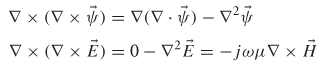
To derive the equations that govern electromagnetic waves propagating in conductive or lossy media, we begin with the loss-free forms of Maxwell’s differential equations presented in Chapter 2 and modify them appropriately to obtain a wave equation that accounts for loss. To begin, the time-harmonic forms of Maxwell’s equations are repeated here:
(2-33)![]()
(2-34)![]()
(2-35)![]()
(2-36)![]()
where ![]() , as derived from equations (2-06) through (2-09).
, as derived from equations (2-06) through (2-09).
Simplification of Ampere’s law (2-34) by replacing the current density term with ![]() yields
yields
(5-1)
Comparison to the solution of Ampere’s law in a loss-free medium (![]() ) allows us to define the complex permittivity for a conductive or lossy media by analogy:
) allows us to define the complex permittivity for a conductive or lossy media by analogy:

where the real component is the dielectric permittivity discussed in Chapters 2 and 3 (![]() ) and the imaginary component accounts for the losses in the medium where the wave is propagating. The term a can be thought of as the conductivity of the material, which will be quite high for a metal and quite low for a dielectric. If (5-2) is inserted into the time-harmonic solution of the electric field derived in Section 2.3.4,
) and the imaginary component accounts for the losses in the medium where the wave is propagating. The term a can be thought of as the conductivity of the material, which will be quite high for a metal and quite low for a dielectric. If (5-2) is inserted into the time-harmonic solution of the electric field derived in Section 2.3.4,
then the complex propagation constant for a lossy media can be derived. The complex propagation constant for a plane wave was derived in Section 2.3.4:
(2-42)![]()
As discussed extensively in Chapter 2, if the wave is propagating in a loss-free medium (where α=0), (2-42) reduces to
where ![]() and
and ![]() Substitution of the complex permittivity (5-2) into (5-3) provides the form of the complex propagation constant of an electromagnetic wave traveling in a conductive medium:
Substitution of the complex permittivity (5-2) into (5-3) provides the form of the complex propagation constant of an electromagnetic wave traveling in a conductive medium:
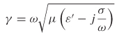
Setting(5-4) equal to 2-42) and separating into real and imaginary components yields the general form of the attenuation constant α and the phase constant β for an electromagnetic wave propagating in a conductive media with a conductivity of ∑:

(5-6)
Note that µ = >µ0 for virtually every practical digital design because the conductors are almost always constructed from copper, which is not magnetic. Both α and β have units of 1/m; however, the dimensionless terms neper (Np) and radian (rad) are used to communicate the attenuation and phase meanings in the wave equation.
5.1.2 Skin Depth
As described in Section 2.3.4, α is the attenuation constant, which will modify a wave propagating in the z -direction as described by
The factor e-αz is known as the wave decay for a wave propagating in the + z-direction. The wave attenuation in a conductive region is governed by the term ![]() , as shown in equation (5-5). As the conductivity of the medium is increased, the attenuation constant α becomes larger and the wave decay increases with distance and time. Consequently, for a good conductor such as copper, the wave will decay very rapidly. The decay of an electromagnetic wave propagating into a conductor is measured in terms of the skin depth. The skin depth, denoted δ, is simply the distance of penetration where the settling exponent -αz of the wave decay factor is -1 (e-αz = e-1). The skin depth is therefore given in units of meters:
, as shown in equation (5-5). As the conductivity of the medium is increased, the attenuation constant α becomes larger and the wave decay increases with distance and time. Consequently, for a good conductor such as copper, the wave will decay very rapidly. The decay of an electromagnetic wave propagating into a conductor is measured in terms of the skin depth. The skin depth, denoted δ, is simply the distance of penetration where the settling exponent -αz of the wave decay factor is -1 (e-αz = e-1). The skin depth is therefore given in units of meters:
Since the term J = aE in Ampere’s law (2-54)) is no longer neglected, a current density J must accompany the electric field E in the conductive region:
(5-8)![]()
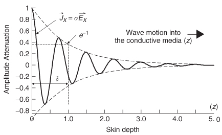
Therefore, at a penetration distance of one skin depth (1/α), the field intensity and the current density have been attenuated by a factor of e-1, or approximately 36.7%, meaning that approximately 63.6% of the current density exists within a distance of 5 from the conductor surface. Note that for a perfect conductor, the conductivity α is infinite and therefore α is also infinite. If α is infinite, equation (5-7) says that δ must be infinitely small. Therefore, for a perfect conductor, the current only flows on the surface and the wave cannot penetrate the conductor. Figure 5-1 shows how the current density decays as the wave propagates into a conductive medium. Note that although the magnitude of the current density is oscillatory, it remains within the envelope defined by the exponential decay of the skin depth.
Figure 5-1 Penetration depth δ associated with the amplitude attenuation of the current density for a plane wave propagating into a conductive region.
If a good conductor is defined such that α/εω»1, (5.5) reduces to
(5-9)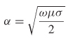
Therefore, the skin depth for a metal with conductivity γ at a frequency ω=2πf is given by (5-10) in units of meters:

Figure 5-2 shows the magnitude of the skin depth in copper as a function of frequency. Note that even at 1 GHz, the skin depth is only 2 µm, meaning that most of the current is flowing in a very small area.
5.2 CLASSIC CONDUCTOR MODEL FOR TRANSMISSION LINES
Classic conductor models are derived on the assumption of perfectly smooth surfaces. Although realistic conductors used to construct printed circuit boards (PCBs), packages, and multichip modules for high-speed digital designs rarely employ smooth conductors, a study of classical transmission-line losses will provide the theoretical basis needed to derive frequency-dependent physically consistent models of real-world conductors, which are often purposely roughened to promote adhesion to dielectric layers during the manufacturing process. The resistive loss induced by general transmission-line conductors can be broken down into two components: low frequency, or dc, and high frequency, or ac. First, the dc losses will be derived and the formulas will be modified to include the frequency-dependent effects of ac resistance at high frequencies.
Figure 5-2 Skin depth α in copper as a function of frequency.

5.2.1 DC Losses in Conductors
Dc losses are of particular concern in small-geometry conductors, very long lines, and multiload (also known as multidrop) buses. Long copper telecommunication lines, for example, must have repeaters every few miles to receive and retransmit the data because of signal degradation. Additionally, designs of multiprocessor computer systems with long buses experience resistive drops that can encroach on the logic threshold levels and reduce the noise margins.
The dc loss of a transmission line depends primarily on two factors: the conductivity of the metal and the cross-sectional area of the conductor where the current is flowing. Figure 5-3 shows the current distribution in a transmission line at dc. Traditionally, dc resistance is defined to be the value at 0 Hz. However, for the purposes of this chapter, dc will be assumed to be valid for all frequencies where the skin depth is larger than the conductor thickness t, which ensures almost uniform current density through the cross section of the signal conductor.
Figure 5-3 Current distribution in a microstrip at dc.
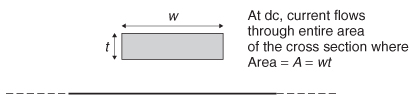
At dc the current will spread out as much as possible and flow through the entire cross section of the conductor, and the resistive loss can be found with
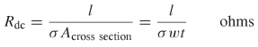
where l is the length, ω the width, t the thickness of the signal conductor, and α the conductivity of the metal. Note that (5.11) has neglected the dc losses of the current return path in the reference plane. This is an adequate approximation because at dc, the current will spread out and flow through the entire plane, which is several orders of magnitude larger than the signal conductor. Consequently, the cross-sectional area where the current flows in the return path will be much larger and the associated resistance will be much smaller.
5.2.2 Frequency-Dependent Resistance in Conductors
By extending the dc equation (5-11), the frequency dependence of the resistance in a transmission line can be approximated. Frequency-dependent resistance will be referred to as ac resistance or skin effect resistance in the remainder of the book. At low frequencies, the ac resistance will be identical to the dc resistance because the skin depth will be much greater than the thickness of the conductor. The ac resistance will remain equal to the dc resistance until the frequency increases to a point where the skin depth is smaller than the conductor thickness.
Figure 5-4 Current distribution in a microstrip with an ideal reference plane at high frequencies where the skin depth δ is small compared to the thickness t .

Microstrip Conductor Losses (Smooth Conductors) Figure 5-4 depicts the current distribution on a microstrip line at high frequencies. Notice that the current distribution is concentrated on the bottom edge of the transmission line. This is because the fields between the signal line and the ground plane pull the charge to the bottom edge, and the skin depth is much smaller than the conductor thickness. Also notice that the current density is greater near the corners of the conductor. This is because the charge density increases significantly in the proximity of a sharp edge, as described in Sections 3.4.4 and 3.4.5, and the current density along the conductor will vary in the same way. Furthermore, there is still significant field concentration along the thickness (the t dimension in Figure 5-4) of the conductor.
The skin effect will cause the cross-sectional area where the current is flowing to decrease as the frequency increases. Consequently, the frequency-dependent losses in the conductor can be approximated using the dc resistance formula by setting t = δ:

Note that the approximation is valid only when the skin depth is smaller than the conductor thickness. Notice that the ac resistance is directly proportional to the square root of the frequency f and inversely proportional to the conductivity δ.
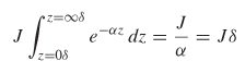
Equation (5-12) assumes that all the current is flowing in the first skin depth, which is not correct. Section 5.1.2 defines the skin depth such that only about 63% of the current density is contained in this depth. To test the validity of equation (5-12), the effective area of an exponential decay can be calculated by integrating e-αz from z = 0 δ to z = ∞ δ and comparing it to the case where all the current is confined to one skin depth. To visualize the differences, refer to Figure 5.5, which plots penetration depth into a conductive medium in terms of skin depths versus the total current density. If 100% of the current is assumed to flow within one skin depth, the area under the curve is J δ = 1, where J is the current density and δ is the skin depth. Integrating the wave decay term e-αz from z = 0δ to z = ∞ δ, the area under the curve also yields J δ:
Since the effective areas under each curve are identical, it is a valid approximation to assume that all the current is flowing in an area confined by the conductor width and a single skin depth. As this section progresses, more accurate methods of calculating the losses will be presented.
Figure 5-5 If all the current is approximated to be in one skin depth, the total area under the curve is identical to the realistic behavior, where the current density decays exponentially with increasing skin depths.

Figure 5-6 Frequency-dependent resistance of a microstrip transmission line with an ideal reference plane.

Figure 5-6 plots the total resistance of a transmission line over a wide fre-quency range. Note that the resistance will remain at approximately the dc value until the frequency where the skin depth is smaller than the thickness of the conductor, after which the ac resistance begins to take effect and increases proportional to ![]() . Note that the discontinuity shown in Figure 5-6 is artificial and drawn for instructional purposes. In reality, current is not completely confined to a single skin depth, so the transition from Rdc to Rac is more gradual and not discontinuous. The discontinuity generally will not have any ill effects on simulated waveforms; however, if it is desirable to smooth the curve to provide more realistic behavior, a root-sum-square function can be used:
. Note that the discontinuity shown in Figure 5-6 is artificial and drawn for instructional purposes. In reality, current is not completely confined to a single skin depth, so the transition from Rdc to Rac is more gradual and not discontinuous. The discontinuity generally will not have any ill effects on simulated waveforms; however, if it is desirable to smooth the curve to provide more realistic behavior, a root-sum-square function can be used:
(5-13)![]()
The resistance of the signal conductor, however, is only one part of the total ac resistance. The portion that is not included in equation (5-12) is the resistance of the return current on the reference plane. The return current will flow underneath the signal line in the reference plane, will be largely concentrated in one skin depth, and will spread out perpendicular to the trace direction with the highest amount of current concentrated directly beneath the signal conductor. Equation (5-14) was derived by Collins [1992] using conformal mapping techniques and shows how the current density varies with increasing distance from the signal conductor center:
Figure 5-7 Current distribution in the reference plane of a microstrip.

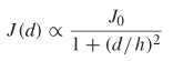
where d is the distance from the conductor center and h is the height above the ground plane and Jo is the total current density. Figure 5-1 is a graphical representation of this current density distribution.
An approximation of the ground plane resistance can be derived using a technique similar to that used to find the ac resistance of the signal conductor. First, assume that all the current will be confined to one skin depth 5. Next, an effective width weff where the current will flow must be determined. Integrating (5.14) from -∞ to +∞ with h = 1,

allows us to determine that (5-14) must be normalized by n so that the total current density is unity for an infinite plane. If the effective width is chosen somewhat arbitrarily at ±3h from the center of the conductor and the normalized current density function is integrated,
(5-15)
it can be shown that about 80% of the total current density is contained within a distance of ±3h of the signal conductors center. Using this approximation,weff = 6h and an approximate formula can be derived for the ground-plane resistance in a microstrip transmission line in units of ohms:

The total resistance is the sum of (5.12) and (5-16) in ohms:

Equation (5-17 ) should be considered a good “back of the envelope” estimation of the ac resistance for a microstrip transmission line [Hall et al., 2000] A more exact formula for the ac resistance of a microstrip was derived using conformal mapping techniques by Collins [1992] and is shown in equation set (5-18). This formula is significantly more cumbersome than (5-17), but should yield the most accurate results.
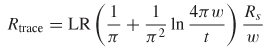
where LR is given by
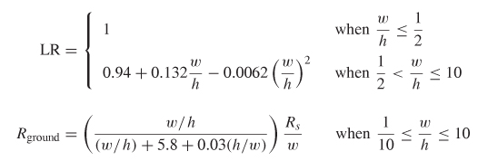
Where

For practical micristrip lines, formulas based on smooth conductors should simply be used as an approximation because realistic conductor surfaces are generally rough, which will increase the conductor losses significantly at frequencies where the skin depth begins to approach the magnitude of the roughness profile. The extra losses caused by surface roughness are calculated in Section 5.3.
Example 5-1 Calculate the approximate frequency where ac resistance must be used to calculate the ohmic losses of a microstrip transmission line constructed with a copper conductor with a conductivity of δ = 5.8 x 10⁷(Ω . m)-1 and the following cross-sectional dimensions: w = 5 mils, h = 3 mils, t = 2.1 mils.
SOLUTION
The ac resistance will exist when the frequency gets high enough so that the skin depth is smaller than the conductor thickness. Above this frequency, dc resistance ceases to exist; only ac (skin effect) resistance is present. The frequency can be calculated by setting a skin depth equal to the conductor thickness using (5-10) and solving for the frequency:
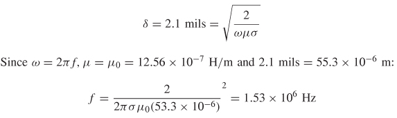
Therefore, at 1.53 MHz, dc resistance does not exist and ac resistance begins to increase with ![]() .
.
Stripline Losses (Smooth Conductors) In a stripline transmission line, the currents of a high-frequency signal are concentrated in the upper and lower edges of the conductor. The current density will be dependent on the proximity of the local reference planes. If the stripline is referenced equidistant from both planes, the current will be divided equally in the upper and lower portions of the conductor as depicted in Figure 5-8. In an offset transmission line, the current densities on the upper and lower edges of the transmission line will be dependent on the relative distances between the ground planes and the conductor (h1 and h2 in Figure 5-8). The current density distributions in each stripline reference plane will be governed by an equation similar to equation
Figure 5-8 Current distribution in the signal; conductor and reference planes of a stripline.

(5-14) and will differ only in the magnitude, which is a function of the respective distances between the reference planes and the strip (h1 and h2). Thus, the resistance of a stripline can be approximated by the parallel combination of the resistance in the top and bottom portions of the conductor. The resistance equations for the upper and lower sections of the stripline may be obtained by applying equation (5-17) or (5-18) for the appropriate value of h. These two resistance values must then be put in parallel to obtain the total resistance for a stripline:
(5-19)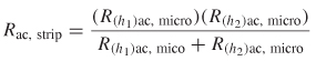
5.2.3 Frequency-Dependent Inductance
Section 5.1 describes how the skin effect will force high-frequency current to flow primarily in a small layer near the periphery of the conductor, and Section 5.2 describes how this translates into frequency-dependent resistance. Another conse-quence of the skin effect is a frequency-dependent inductance. To conceptualize where this frequency dependence comes from, consider two filaments of current that form a loop with the return plane immediately below the conductor over a differential length of transmission line Δz, as depicted in Figure 5-9. Loop (a) passes through the center of the signal conductor, and loop (b) exists only on the conductor surfaces. As described in Section 2.5.2, the inductance is proportional to the loop area,
(2-97)
where ψ1 is the magnetic flux, which depends on the loop area. Therefore, loop (a) will have a higher inductance than loop (b) simply because the loop is larger. At low frequencies, the skin depth will be large compared to the conductor thickness and there will be significant current flowing in the interior of the conductor
Figure 5-9 Loops for a filament of current: (a) in the center of the conductor; (b) on the surface of the conductor.
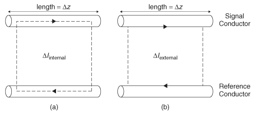
As frequency increases, the skin effect causes the current to flow very close to the surface, with minimal current flowing interior to the conductor. At infinite frequencies, all the current is flowing on the surface and the internal contribution is zero. Consequently, as frequency increases, the effect of Linternal will decrease and Ltotal will asymptote to Lexternal.
The external inductance is calculated with quasistatic techniques assuming that all the charge is on the surface of the conductor and solving Laplace’s equation as shown in Sections 3.4.2, 3.4.3, and 3.4.6. The internal inductance is derived by observing Ampere’s (2-34) and Faraday’s (2-33) laws for a good conductor. For a good conductor, the conduction current ![]() will be much larger than the displacement current jω
will be much larger than the displacement current jω![]() , and therefore Ampere’s law reduces to
, and therefore Ampere’s law reduces to
Faraday’s law is repeated here:
(2-33)![]()
Taking the curl of (2-33) yields the following equation:
(5-22)![]()
If it is assumed that the free charge is negligible and the source of the electric field is the time-varying magnetic field, Gauss’s law reduces to Δ·ε=0, allowing the use of the vector identity (see Appendix A)
to simplify the equation, which reduces to
Substituting Ampere’s law (5.21) into (5-23) and multiplying each side by δallows us to write (5-23) in terms of the current density (since![]() )=δ
)=δ![]() :
:
Equation (5-24) is known as the diffusion equation for the current density. Similar equations govern the electric and magnetic fields. Assuming a z-directed current, the solution to (5-24) is found using standard techniques.
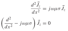
The roots of the characteristic equation yield

Comparing to equation (5-10), note that ![]() , giving a solution to the diffusion equation for current density of
, giving a solution to the diffusion equation for current density of
where only the negative exponent is a valid solution because the current density decreases as the electromagnetic wave penetrates into the conductor. Equation (5-25) says that the current density will decrease very rapidly into the surface of the conductor and is essentially confined to a layer at the surface equal to a few skin depths, as depicted in Figure 5-1.
The total current can be found by integrating (5.25):(5-26)
Figure 5-10 Diffusion of currents into a semi-infinite conductive material.
The surface impedance can be defined as the ratio of the electric field at the surface and the total current density:
(5-27)
Substituting (5-26) into (5-27) and expressing the current density in terms of the conductivity and the electric field (![]() 0 = δ
0 = δ![]() 0) yields
0) yields

The surface impedance is expressed in terms of an area of unit width and unit length, so the term ohms/square is used. Note the similarity of the real part of (5-28) to equation (5-12), which was the series resistance caused by the skin effect of a transmission line. For the case where l = ω, the real part of equations ( 5-28) and (5-12) are identical. If the real part of (5-28) is resistance, the imaginary part must therefore be reactance (the impedance of inductance). Since the impedance of inductance is joL, (5-28) can be expressed in terms of a series resistance (due to the skin effect) and a series inductance (the internal inductance):
(5-29)![]()
Therefore, the internal inductance can be calculated directly from the ac resistance:
Equation (5-30) highlights an important relationship between the skin effect resistance (ac resistance) and the internal inductance. As the skin effect forces the current to the periphery of the conductor, the resistance increases; however, since current ceases to flow in the interior of the conductor, the inductance must decrease. Figure 5-11 plots both the internal inductance and the ac resistance. Note that when the ac resistance becomes significant, the internal inductance is almost negligible.
Example 5-2 Calculate the total inductance and the resistance at 2 GHz of a microstrip transmission line constructed with copper of conductivity 107(Ω·m)-1, a dielectric constant of εr and the following cross-sectional dimensions: t = 0.5 mil, h = 2 mils, #x03C9; = 3 mils.
SOLUTION
Step 1: Determine if the ac or dc resistance should be used. The methodology presented in Example 5-1 could be used, however, it is easier simply to calculate the skin depth in copper at 2 GHz using (5-10) and compare it to the conductor thickness t:
Figure 5-11 Example of how the skin effect changes resistance and internal inductance with frequency for a copper microstrip as shown in Figure 5-6.

Since t = 0.5 mil = 12.7 µm, δ < t, so the ac resistance must be used.

Step 2: The impedance and effective dielectric permittivity must be calculated using equation (3-36b), which assumes a perfect conductor. If it is unknown whether a particular impedance formula includes the effect of a realistic conductor, the lack of a metal conductivity or a magnetic permeability variable indicates the assumption of infinite conductivity. From (3-36b), z0≈55 ω and εeff≈2.95
Step 3: Calculate the phase velocity with (2-52):

Step 4: The external inductance is solved with (3-31) and (3-33) Since ((3-36b)) assumes a perfect conductor, the inductance is the external value.

Step 5: Calculate the ac resistance at 2 GHz using (5-17). Note that (5-18) could be used as well.

Step 6: Calculate the internal inductance using (5-30).
Step 7: Calculate the total inductance using (5-20).
![]()
5.2.4 Power Loss in a Smooth Conductor
In high-speed digital design, surface treatment of the copper foils used to construct printed circuit boards (PCBs) significantly affects the power losses experienced by a signal propagating on a transmission line. In this section, the power losses of an electromagnetic wave impinging on a flat, smooth plane are examined. In later sections we explore the consequences of rough conductor surfaces.
First, we assume that the fields in the vicinity of a good but not perfect conductor will behave approximately the same as for a perfect conductor. In Section 3.2.1 it was shown that the electric fields terminate normal to a perfect conducting surface and the magnetic fields are tangential to the surface. Furthermore, in Section 5.1.2 it was shown that fields inside a conductor will attenuate exponentially and are measured in terms of the skin depth δ. At high frequencies, the boundary condition shown in (3-33) is true for a good conductor, except for a thin transitional layer.
To derive an equation to predict the loss for a smooth plane, we first assume that just outside the conductor there exists only a normal component of the electric field (![]() ±) and a tangential component of the magnetic field(
±) and a tangential component of the magnetic field(![]() ll), which are the identical boundary conditions used for perfect conductors. Following the approach outlined by Jackson [1999], Maxwell’s equations are then used to calculate the fields within the transition layer.
ll), which are the identical boundary conditions used for perfect conductors. Following the approach outlined by Jackson [1999], Maxwell’s equations are then used to calculate the fields within the transition layer.
If a tangential Hy exists just outside the surface, the same Hy must exist just inside the conductor surface. With the neglect of the displacement current, (2-33) and (2-34) become
(5-31)![]()
(5-32)![]()
where ![]() c and
c and![]() c denote the field values inside the conductor. If it is assumed that n is the normal vector pointing outward from the conductor surface and z is the normal coordinate inward into the conductor, the gradient operator is
c denote the field values inside the conductor. If it is assumed that n is the normal vector pointing outward from the conductor surface and z is the normal coordinate inward into the conductor, the gradient operator is ![]() reducing Maxwell’s equations to
reducing Maxwell’s equations to


These equations can be solved to yield the fields inside the conductor. The first step is to take the partial derivative of (5-34):

Next is to take the cross product of (5-33) with the unit vector,
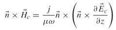
so the vector identity from Appendix A can be used to simplify the math,
where![]() because when (5-35) is substituted, the form becomes proportional to
because when (5-35) is substituted, the form becomes proportional to![]() which is zero. Furthermore,
which is zero. Furthermore,![]() , yielding
, yielding

Next, equation (5-35) is substituted for![]() yielding
yielding

After rearranging the equation, we get a more manageable form:

Since![]() , the equation can be written in terms of the skin depth,
, the equation can be written in terms of the skin depth,
![]()
which yields the differential equation

To solve (5-36), we reasonably assume that the field inside the conductor is a function of the external applied field,

where f(z=0)=1, which says that at the surface of the conductor, ![]() This allows us to substitute (5-37) into (5-36) and solve the equation for f (z).
This allows us to substitute (5-37) into (5-36) and solve the equation for f (z).

The solution to (5-38) is
![]()
wheref(z=0)=1=A, yielding
(5-39)![]()
where![]() is the tangential magnetic field applied to the surface of the conductor. The electric field inside the conductor is calculated from (5-34):
is the tangential magnetic field applied to the surface of the conductor. The electric field inside the conductor is calculated from (5-34):
Since the tangential component of the electric field must remain continuous, as shown in equation (3-8), the electric field just outside the conductor surface can be calculated with (5-40) evaluated at z = 0:
Section 3.2.1 says the electric field must terminate normal to a perfectly conducting surface, however, equation (5-41) shows that for a good conductor, a tangential component of ![]() must exist just outside the conductor. Since (5-40) describes the electric field decaying with increasing depth z into the surface, there must be power flow into the conductor. The time-averaged value of the Poynting vector described in Section 2.6.1 is used to calculate the power absorbed per unit area:
must exist just outside the conductor. Since (5-40) describes the electric field decaying with increasing depth z into the surface, there must be power flow into the conductor. The time-averaged value of the Poynting vector described in Section 2.6.1 is used to calculate the power absorbed per unit area:
(2-121)
The intrinsic impedance (2-53) at the surface of the conductor, 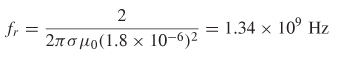 , is calculated with (5.37) and (5.41):

It is interesting to note that since  (5-42) reduces to equation (5-28), which is the series impedance of a transmission line:
Finally, the power flow per unit area into the conductor is calculated using equation (2-121):

From (5-10), ![]() , yielding (5-43) , which is the time-averaged power absorbed by a flat conducting plane per unit area:
, yielding (5-43) , which is the time-averaged power absorbed by a flat conducting plane per unit area:

Equation (5-43) will allow for the solution of the resistive power losses of a good conducting plane provided that the applied magnetic field ![]() has been solved for the idealized case of a perfect conducting plane.
has been solved for the idealized case of a perfect conducting plane.
The power loss from a plane can also be put in more intuitive form. Equation (2-07), which is simply Ohm’s law, can be used to calculate the current density from (5-40):
Again, since![]() the equation can be rewritten as
the equation can be rewritten as

Equation (5-44) simply says that most of the current density will be confined to a very small thickness, as described in Section 5.1.2. Note that the cross product in(5-44) implies that the current will flow perpendicular to the magnetic field.
To derive a more intuitive form of the power dissipated by a flat plane, it is first necessary to define an effective surface current. If the current density (5-44) is integrated to get the total current, an equivalent surface current can be calculated for use in the classic time-averaged power equation![]()

Equation (5-45) simply calculates the total current that is decaying exponentially into the conductor surface. To calculate the power per unit area, we make the approximation that all the current exists on the surface and use the real part of the surface impedance in (5-28):
(5-46)
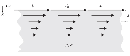
5.3 SURFACE ROUGHNESS
To account properly for the frequency variation of Linternal and Rac, the nonideal effects of the copper surface must be considered. The problem is that most (if not all) commercial 2D field solvers calculate the resistance and inductance assuming smooth conductors. Real copper surfaces, however, are purposely roughened to promote adhesion to the dielectric when manufacturing printed circuit boards. The resulting copper surfaces have a “tooth structure” as depicted in Figure 5-12. When the tooth height is comparable to the skin depth, the smooth copper assumptions break down. The root-mean-square (RMS) tooth height of common copper foils used to manufacture printed circuit boards range from approximately 0.3 to 5.8 µm, with peak heights exceeding 11 µm [Brist et al., 2005]. The skin depth in copper at 1 GHz is about 2 µm, indicating that for many copper foils, most of the current will be flowing in the tooth structure for multigigabit designs [Hall et al., 2000]. Since the rough copper surface affects current flow, it will also affect power dissipation, and thus insertion loss is.
Figure 5-12 Realistic conductors used to manufacture transmission lines exhibit a rough surface often called the “tooth structure.” When the skin depth is similar to the tooth size, power dissipation is increased.

Insertion loss, which is described extensively in Chapter 9, is a common way to measure the frequency-dependent losses in the form of a transfer function by injecting a sinusoidal waveform at port 1 (such as the input to a transmission line) and measuring at port 2 (such as the output). Expressed in terms of power, the insertion loss is
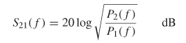
where S21 is the insertion loss in decibels, P2 is the power measured at the output of the transmission line, and P1 is the power injected into the input of the transmission line. Insertion loss is a convenient method to evaluate the power loss of a transmission line. Note that the ratio of powers reduce to a ratio of voltages when the port impedances are identical, as shown in equation (9-21), which is why the form 20 log is used instead of 10 log to calculate the magnitude in decibels [Hall et al., 2000].
Figure 5-13 shows the measured results of two identical transmission lines built with rough and relatively smooth copper. The copper foil used to construct the test boards was characterized with an optical profilometer prior to lamination yielding an RMS tooth height of hRMS = 1-2 µm for the smoother copper and hRMS = 5.8 µm for the rough copper. Note the significant increase in insertion losses, and therefore power losses, due to increased roughness profile. At high frequencies, surface roughness will increase the ohmic losses of a transmission-line conductor significantly.
5.3.1 Hammerstad Model
The traditional way to account for surface roughness losses in a transmission-line model is to use the Hammerstad equation:
Figure 5-13 Measured results of identical 7-in. transmission lines with relatively smooth (µRMS = 1-2 µm) and rough (hRMS = 5.8 µm) copper showing how surface roughness affects losses.

where ![]() is the classic skin resistance for a smooth conductor as calculated in (5-17) and (5-18) and KH is the Hammerstad coefficient:
is the classic skin resistance for a smooth conductor as calculated in (5-17) and (5-18) and KH is the Hammerstad coefficient:
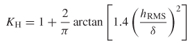
Where hRMS is the root-mean-square value of the surface roughness height and δ is the skin depth [Hammerstad and Jensen, 1980; Brist et al., 2005]. The Hammerstad coefficient is used to model the extra losses caused by the copper surfaces on a transmission line that are often purposely roughened to promote adhesion to the dielectric.
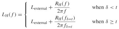
The frequency dependence of the skin effect resistance and total inductance using the Hammerstad correction for surface roughness is implemented with†
(5-49a)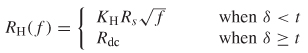
†Note that the method shown here for calculating the internal portion of the inductance (Linternal = Rac/ω)for a rough conductor is an approximation based on the result for a smooth conductor. The approximation will induce causality errors that tend to be small enough to ignore, so this method is generally acceptable. For the interested reader, Appendix E derives the internal inductance using a more rigorous approach based on the discussion in Chapter 8.
where KH is calculated with (5-48), t is the conductor thickness, δ the skin depth, and fδ=t the frequency where the skin depth equals the thickness of the conductor. When the skin depth (δ) is larger than the conductor thickness, the dc value of the resistance and low-frequency inductance where the skin depth is equal to the conductor thickness should be used.
This approach has been shown to be accurate by comparison to vector network analyzer measurements of insertion loss for copper surface roughness profiles less than approximately 2 µm (RMS). Figure 5-14 shows the accuracy of the Ham- merstad model by comparing measured transmission-line structures constructed with relatively smooth and very rough copper to simulations using (5-49). Notice that the Hammerstad model is considerably less accurate for the rough copper case for frequencies greater than about 5 GHz.
To understand why the accuracy breaks down for some copper types, it is useful to explore the assumptions behind (5-48), which assumes a 2D corrugated surface similar to that shown in Figure 5-15 [Pytel, 2007]. The first published work providing a theoretical investigation into the power loss from copper roughness was in 1948 by Samuel Morgan (Bell Laboratories), who studied the effects up to 10 GHz providing loss equations for current flow transverse and parallel to corrugated structures similar to that depicted in Figure 5-15. He concluded that power loss is proportional to the surface area of the roughness structure, current flow transverse to the corrugated surface could increase the power losses by 100%, and current flow parallel to the grooves increases losses by about 30%. In 1975, a Norwegian scientist named Erik Hammerstad used Morgan’s work to fit the data to an arctan function, producing the Hammerstad equation shown in (5-48), which became the standard equation in industry to account for the effects of surface roughness [Pytel, 2007]. The model assumes that at high frequencies, when the skin depth becomes small compared to the tooth height, the current will begin to follow the contour of the corrugated surface, which will increase the losses.
Figure 5-14 Example of the Hammerstad model accuracy for (a) relatively smooth (h RMS = 1.2 µm) and (b) rough (h RMS = 5.8 µm) copper foils; 7-in. microstrip line.
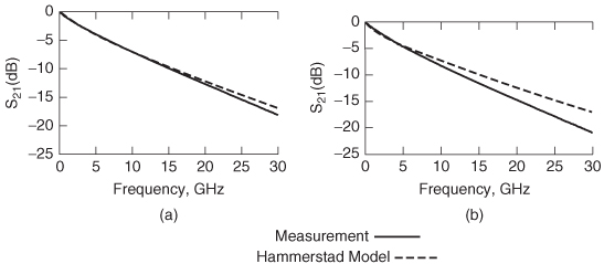
Figure 5-15 Two-dimensional corrugated surface assumption behind the Hammerstad equation.

To understand why the Hammerstad equation breaks down for some roughness profiles, the surfaces of relatively smooth and rough copper surfaces were measured using an optical profilometer. The surface shown in Figure 5-16a [Hall et al., 2007] can be described as corrugated with sparse protrusions on the surface, suggesting that the Hammerstad equation (5-48) might be adequate for approximating the surface roughness losses for a transmission line manufactured with this copper foil. Figure 5-14a depicts a measurement of a transmission line that was constructed with the copper foil depicted in Figure 5-16a compared to a model created using (5-47) and (5-48). Note that the model and measurement correlate very nicely until about 15 GHz, indicating that the Hammerstad model is adequate to model the losses for this case.
Figure 5-16 Surface profile measurement of (a) relatively smooth and (b) rough copper foil used to construct PCBs.
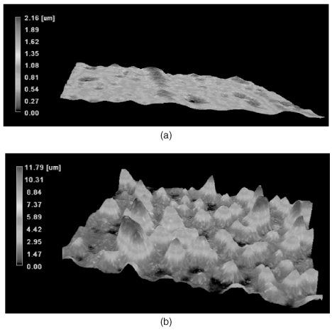
Conversely, Figure 5-16b depicts an optical profilometer measurement of a very rough copper foil. Note the significant difference between the corrugated surface assumed by the Hammerstad equation and the surface depicted in Figure 5-16b, suggesting that (5-48) will not work well for this type of 3D surface profile. Figure 5-14b depicts the measurement of a transmission line constructed with the rough copper sample shown in Figure 5-16b compared to a model created with (5-47) and (5-48). Note that the accuracy breaks down after about 5 GHz, indicating that an alternative modeling methodology is needed for losses induced by this surface profile.
Example 5-3 Assuming the transmission line in Example 5-2, calculate the frequency where surface roughness begins to affect the losses for an RMS tooth height of 1.8 µm, calculate the ac resistance and total inductance at an operating frequency of 2 GHz, and determine how surface roughness changes the resistance and inductance compared to the smooth case.
SOLUTION
Step 1: To determine the approximate frequency where the surface roughness will begin to affect the ac losses, the skin depth must be set equal to the RMS roughness height, and the frequency is calculated using (5-10):
Since this is close to the operating frequency of 2 GHz, the surface roughness will be significant and cannot be ignored. Note that the roughness will influence the losses at frequencies below fr; however, if fr» f, the surface roughness will have no significant effect, and it can be ignored.
Step 2: Calculate the ac resistance at 2 GHz using (5-47) and (5-48). The ac resistance at 2 GHz for a smooth surface was calculated in Example 5-2.
Since the RMS roughness height is less than 2 µm, (5-48) is suitable to correct the smooth formula to estimate the extra losses due to the rough surface.


Therefore, the ac resistance including the surface roughness is
![]()
Step 3: Calculate the internal inductance using (5-30).
![]()
Step 4: Calculate the total inductance using (5-20), where Lexternal is as calculated in Example 5-2.
![]()
Step 5: Compare the values to the smooth case in Example 5-2. Note that the surface roughness increases the resistance and internal portion of the inductance significantly compared to the identical values for a smooth conductor from Example 5-2.

5.3.2 Hemispherical Model
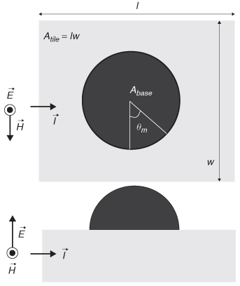
The rough surface depicted in Figure 5-16b can be characterized as random protrusions sitting on a flat plane, which precludes rigorous derivation of an analytical formula to calculate the extra losses due to current flowing in the tooth structure. Subsequently, for the rough copper, an approximation of the tooth structure is required so that an analytical solution can be derived. As a first approximation, a hemispherical boss sitting on a plane can be used to represent the individual surface protrusions as shown in Figure 5-17 [Hall et al., 2007]. The complete surface is modeled using N hemispheres randomly distributed on a flat plane. A TEM (transverse electromagnetic) wave is assumed incident on the hemisphere at a grazing angle of 90° with respect to the flat plane and with the H field (the magnetic field intensity) tangential to the surrounding plane as shown in Figure 5-17. To find the power dissipated by the structure, the absorption and scattering of the incident TEM wave on the hemisphere must be calculated. The problem of scattering of a plane wave from the hemispherical protrusion on the flat surface can be approximated using superposition. First the power losses of a sphere are calculated and then divided in half because the structure is a hemisphere, and then the power loss of the flat plane surrounding the hemisphere is calculated. The total power dissipated is then calculated simply by adding the results.
Figure 5-17 Simplified hemispherical shape approximating a single surface protrusion: top and side views; current direction and applied TEM field orientations shown.
For a good conducting protrusion (as opposed to a perfect electrical conductor protrusion) a plane electromagnetic wave incident on a conducting sphere will be partly scattered and partly absorbed. The total power scattered and absorbed from a sphere divided by the incident flux is known as the total cross sectionand is calculated by Jackson [1999] (with units of square meters) as

where![]() is the speed of light, and the scattering coefficients are approximated assuming that kr « 1, where r is the sphere radius, and are given by [Jackson, 1999]
is the speed of light, and the scattering coefficients are approximated assuming that kr « 1, where r is the sphere radius, and are given by [Jackson, 1999]
The Poynting vector, which was described in Section 2.6, gives the power of an electromagnetic wave in units of watts per square meter:

Subsequently, the total power absorbed or scattered is calculated by multiplying (5-50) and (5-52) and dividing by 2 so the results are for that of a hemisphere:

where ![]() and H0 is the magnitude of the applied magnetic field. Note that reasonable accuracy (at least up to 30 GHz) can be obtained when only the first term (m = 1) in (5-50) is considered when calculating (5-53).
and H0 is the magnitude of the applied magnetic field. Note that reasonable accuracy (at least up to 30 GHz) can be obtained when only the first term (m = 1) in (5-50) is considered when calculating (5-53).
Equation (5-53) calculates the power loss of a hemisphere. Now, the losses of the flat plane surrounding the protrusion must be accounted for. The time-averaged power absorbed by a flat conducting plane per unit area is calculated from equation (5-43):

To approximate the losses of a single hemispherical boss sitting on a flat plane of finite conductivity, the power loss of the hemisphere is added to the loss of the plane less the base area of the hemisphere:

where Atitle is the tile area of the plane surrounding the protrusion (see Figure 5-17) and Abase is the base area of the hemisphere. Note that (5-55) is an approx-imation because it assumes that the magnetic field (HO) on the tile is not affected by the presence of the hemisphere and the loss of the surrounding plane is simply a function of the area.
To gain an intuitive understanding of how a propagating electromagnetic wave behaves in the presence of a protrusion, it is useful to observe the fields and solve for the surface currents on a PEC (perfect electrical conducting) sphere, which is a good approximation of how the current will flow at very high frequencies when the skin depth is small compared to the sphere. In Section 3.2.1 the boundary conditions for a PEC were described; the electric field must emanate from and terminate normal to a perfectly conducting surface, and the magnetic field must be tangential to the conductor surface. First consider Figure 5-18a, which depicts the front cross-sectional view of a hemispherical protrusion sitting on a conducting plane where the current flow is out of the page. Note that the electric fields are drawn perpendicular to the conductor surface and the magnetic fields are tangent
Figure 5-18 (a) Front view of fields and current showing the normal electric field and tangential magnetic field; (b) current streamlines flowing over the top of a single surface protrusion.
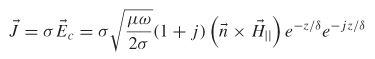
to the surface. Figure 5-18b shows the top view of the same protrusion with the current flowing from the left to the right. If TEM is assumed, the magnetic field will be perpendicular to the electric field as described is Section 2.3.2. The magnetic field intensity lines depicted in Figure 5-18b are those near the surface of the plane and not on the sphere. Note that these fields bend around the protrusion because they must satisfy the boundary conditions and remain tangent to the PEC hemisphere. Furthermore, equation (5-44) says that lines of constant magnetic field intensity are orthogonal to the lines of surface current flow, indicating that if the magnetic field bends around the hemisphere, an area of low current density perpendicular to the current flow will be induced. The surface current density on the hemisphere (Jeff) (in A/m2) can be derived by defining the magnetic field in terms of a magnetic scalar potential [Orlando and Delin, 1991; Huray et al., 2007; Huray, 2008]:
where θm is the angle between the applied magnetic field and the current flow (see Figure 5-17). If the uniform current streamlines on the plane are matched with those calculated with (5-56), the influence of a hemisphere sitting on a plane can be observed. Figure 5-18b depicts how current will flow in the presence of a spherical protrusion. Note that the current on the flat portion of the plane is drawn toward the protrusion with the highest density on the top and minimal current density on the side perpendicular to the current flow. The current crowding at the top of the protrusion effectively decreases the area where current flows, increases the path length, and thus helps explain the physical mechanisms that cause extralosses on a rough surface. It also appears to support Morgan’s claim that the surface area is the key factor to surface roughness losses.
To calculate a new correction factor for use in (5-47), the ratio of the power absorbed with and without a good conducting protrusion present must be derived. This is accomplished simply by dividing (5-55) by (5-54):
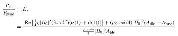
This equation can be simplified to eliminate the variable of the magnetic field, yielding

Note that (5-57) becomes invalid when the skin depth is greater than the surface protrusion height. At these frequencies the power dissipated by a flat plane with an area equal to the base of the protrusion will be greater than the power dissipated by the protrusion. Subsequently, a knee frequency can be defined when Ks = 1, where the roughness begins to affect the losses significantly. Below the knee frequency, the correction factor, Ks, is unity. Subsequently, implementation of this correction factor is shown as

To implement (5-58) accurately, the surface shown in Figure 5-16b must somehow be represented by equivalent hemispheres. The additional surface area of simple hemisphere bosses are insufficient to account for the measured surface roughness losses. This is not surprising when one compares the additional hemisphere model area to the 3D surface of the rough copper sample shown in Figure 5-16b. To account for additional surface area the root mean square (RMS) volume of the rough surface must be calculated, and volume equivalent hemispheres are created to determine Abase. The RMS distance between peaks in the roughness profile is used to calculate the tile area, Atitle To obtain these input parameters, the surface is measured using a profilometer, as shown in Figure 5-19. To facilitate the volume equivalent model, the tooth shape is approximated as one-half of a prolate spheroid instead of a hemisphere, because it more closely resembles the shape of the protrusion. A prolate spheroid is a surface of revolution obtained by rotating an ellipse about its major axis. A symmetrical egg (i.e., with the same shape at both ends) would approximate a prolate spheroid
Figure 5-19 Example of a surface profilometer measurement of a rough copper sample showing peak heights that range from 0.7 to 8.5 µm. The flat surface is assumed to be at 0.5 µm.

[Mathworld, n.d.]. The spheroid volume is in turn equal to one-half the volume of a sphere to calculate the radius of a hemisphere with the same volume as the hemispheroid-shaped surface protrusion:

where bbase is the tooth base width, htooth the tooth height, and re the radius of a hemisphere with equivalent tooth volume. The base area of the hemisphere, Abase is then calculated:
(5-60)
The square tile area of the surrounding flat plane is calculated based on the distance between peaks:
If the RMS values of dpeaks, htooth and bbasevalues are calculated, the surface shown in Figure 5-16b and measured in Figure 5-19 can be represented as the equivalent surface in Figure 5-20.
A comparison between the correction factor calculated from the Hammerstad model (5-48) and the hemispherical model (5-58) with the modified equivalent volume is shown in Figure 5-21. Note that the hemisphere model saturates at a much higher value than Hammerstad, which will always saturate at a value of 2. The implementation shown in (5-58) causes a nonphysical discontinuity at the frequency where the model transitions from dc to ac behavior, which is the point where the surface of the flat plane with an area equal to the base of the hemisphere has more loss than the hemisphere. Some engineers may be concerned that the discontinuity may induce nonphysical glitches into the time-domain responses. However, simulations of pulses as fast as 30 Gb/s were
Figure 5-20 Equivalent surface represented by hemispheres with the same RMS volume as that of the measured surface profile.
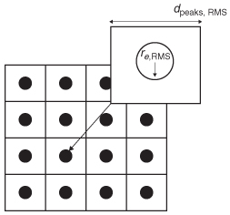
Figure 5-21 Hammerstad correction factor (5-48) compared to the hemisphere model (5-58). RMS roughness: ftRMS = 5.8 µm, rfpeaks,RMS = 9.4 µm.

performed using this method in HSPICE and Nexxim with no apparent nonphys- ical aberrations observed.
The frequency dependence of the skin effect resistance and total inductance using the hemisphere correction for surface roughness is implemented with (5-62a) and (5-62b).† When the skin depth δ is larger than the conductor thickness (which includes the roughness profile), the dc value of the resistance and low-frequency inductance where the skin depth is equal to the total conductor thickness should be used:
† Just as with equation (5-49b), the method shown here for calculating the internal portion of the inductance (Linternal = Rac/ω) for a rough conductor is an approximation based on the result for a smooth conductor. The approximation will induce causality errors that tend to be small enough to ignore, so this method is generally acceptable. Appendix E derives the internal inductance using a more rigorous approach based on the discussion in Chapter 8.
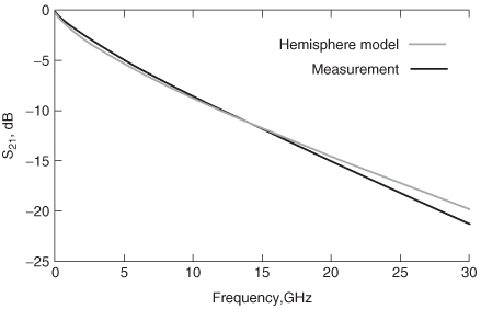
Figure 5-22 Accuracy of the hemisphere surface roughness model (5-58); 7 in. microstrip; εr tan S = 3.9/0.0073 at 1 GHz; RMS roughness of copper foil hRMS = 5.8 µm, dpeaks,RMS = 9.4 µm. (Adapted from Hall et al. [2007].)


Where Khemi is calculated with (5-58), t is the conductor thickness, >δ is the skin depth, and fδ=t is the frequency where the skin depth equals the thickness of the conductor.
Figure 5-22 depicts the accuracy of the hemisphere model for very rough copper. The small deviation that occurs between the model and the measurement in Figure 5-22 is because (5-57) essentially uses superposition to combine the losses of the tile and protrusion and does not account for the interaction between the hemisphere and the plane. Consequently, the formula is very accurate (1) at low frequencies where the skin depth is large compared to the protrusion and the loss is due primarily to the plane, and (2) at high frequencies where the skin depth is small compared to the protrusion and the loss is due primarily to the roughness. At intermediate frequencies, where the skin depth is on the same order as the roughness height, an error is introduced. Additionally, the roughness shape was approximated with a spheroid and the interactions between spheres were neglected. Nonetheless, for very rough copper surfaces, Figure 5-22 shows that the methodology produces very reasonable accuracy over a wide bandwidth with a simple, easy-to-use formula. More important, it provides valuable intuition into the mechanisms that cause surface roughness losses.
Note that the method of calculating the surface roughness correction factor K should be chosen carefully. If relatively smooth copper is being used, witha RMS value of the surface roughness less than about 2 µm, Hammerstad’s formula (5-48) has been shown to adequately approximate the surface roughness losses. However, for very rough copper (which is often preferred by PCB vendors due to its decreased tendency of delaminating), equation (5-58) using equivalent volume hemispheres will approximate the surface roughness losses with more accuracy.
Example 5-4 Calculate the surface roughness correction factor of the microstrip transmission line in Example 5-2 at 5 GHz. The RMS value of the tooth height htooth = 5.8 µm, the RMS base width of the tooth structures is bbase = 9.4 µm, and the distance between peaks dpeaks = 9.4 µm.
SOLUTION
Step 1: Use equations (5-59) through (5-61) to calculate a sphere with the same volume as a spheroid-shaped surface protrusion:

Note that the diameter of the equivalent volume hemisphere (10 µm) is actually larger than the edge length of the tile (9.4 µm), meaning that the hemispheres will overlap. This is not a concern since it is understood that the surface roughness shape is not hemispherical in nature and the shape of the protrusion is assumed to be a spheroid. However, the equivalent volume hemisphere allows for a much simpler solution to the electromagnetic fields without sacrificing much accuracy.
Step 2: Use (5-57) to calculate the correction factor at 5 GHz. To calculate the intrinsic impedance rj = V/’oA’oµ’- the value of the dielectric permittivity directly under the rough surface should be used and not the effective value for the microstrip as calculated in Example 5-2.

For this example, it can be shown that / (1) is negligible, so it is ignored.
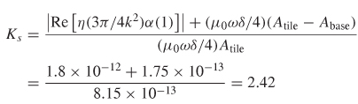
In this case, the series resistance of a transmission line manufactured with a cop-per conductor with this roughness profile would be approximately 2.42 times as high at 5 GHz as the same transmission line constructed with a smooth conductor.
5.3.3 Huray Model
In 2006 at the University of South Carolina, Paul G. Huray was researching new wideband modeling techniques for surface roughness that would provide better accuracy than both the Hammerstad and hemisphere models. Upon observation of scanning electron microscope (SEM) photographs of copper foil samples used to manufacture printed circuit boards (PCBs), he observed that the structures appeared to be constructed of conducting “snowballs,” as shown in Figure 5-23. Subsequently, he formed a material and physical basis of a theoretical model that is composed of a distribution of spherical shapes [Olufemi, 2007; Hurray, 2009].
Printed circuit boards are a “stackup” of layers of copper conductors and inter-vening layers of an insulating propagating medium such as FR4 joined under heat and pressure. To assure that the copper sheets do not delaminate from the dielectric layers, manufacturers typically electrodeposit an additional surface layer of copper on a relatively smooth copper foil that creates irregular features as large as 11 µm, to promote good adhesion. The electroplated copper produces a surface
Figure 5-23 SEM photograph of rough copper at 5000 x magnification at a 30° angle.

roughness profile that can be described as spherical particles, joined together in a network to form a distorted surface, as shown in Figure 5-24. An individual snowball is located a distance x below a flat copper surface, has radius ai, and, when it experiences an external electromagnetic field intensity, as it would in the region below the copper trace when a signal is propagating on a transmission line, it will dissipate power similar to the hemisphere described in equation
Figure 5-24 Cross section of a distribution of copper spheres that create a 3D rough surface in the form of copper “pyramids” on a flat conductor.*

(5-53) with twice the magnitude since it is a whole sphere:
(5-63)
For a distribution of copper spheres such as the pyramidal configuration that creates 3D copper roughness profiles shown in Figures 5-23 and 5-24, superposition of the sphere losses can be used to calculate the total losses of the structure [Olufemi, 2007; Huray, 2009]. Since roughness losses are proportional to the surface area of the tooth structure, the number and size of the spheres can be chosen to approximate the surface roughness correction factor very accurately. To do this, the general tooth shape must be approximated, the average snowball size must be measured, and the number of spheres that correspond to the surface area of the protrusion must be calculated. If SEM photographs are analyzed extensively, it may be possible to build a model with multiple snowball sizes that very closely replicated the actual tooth shape. However, since electron microscopes are typically not available, profilometers will provide approximate tooth shapes, and a reasonable model can be constructed.
The total power dissipated by the tooth structure is simply the sum of the power dissipated from the total number of spheres (N) required to replicate the surface area of the tooth structure:
(5-64)
To calculate a new surface roughness correction factor for use in (5-47), the ratio of the power absorbed with and without surface roughness must be derived using (5-65) and (5-54):
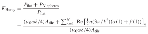
To calculate the total number of spheres(N) needed to represent the surface area of the roughness profile, it is useful to choose a geometric shape that resembles a typical tooth. If one-half of a spheroid (a hemispheroid) is chosen as the approximate tooth shape, laboratory data indicate that reasonable accuracy can be obtained. However, the SEM photograph in Figure 5-23 clearly shows that a spheroid is only an approximation because the real tooth shape has more surface area. Consequently, this assumption is expected to slightly underpredict the surface roughness losses at high frequencies. A detailed statistical analysis of theSEM photograph could provide a more accurate representation of the specific size and number of spheres; however, the spheroid assumption produces reasonable results compared to measured surfaces.
To construct a Huray surface roughness model, the surface is measured as in Figure 5-19 and the RMS values of bbase and htooth are calculated. Next, the surface area of a hemispheroid is calculated with a base bbase and a height htooth. An appropriate snowball radius is chosen (usually between 0.5 and 1 µm), and the total number of copper spheres (N) are calculated so that the total surface area of all N spheres is equal to that of the hemispheroid constructed using the RMS values measured with the profilometer. The procedure is demonstrated with the following example.
Example 5-5 Calculate the surface roughness correction factor using the Huray equation at 5 GHz. The RMS value of the tooth height htooth = 5.8 µm, the RMS base width of the tooth structures bbase = 9.4 µm, and the distance between peaks dpeaks = 9.4 µm.
SOLUTION
Step 1: Calculate the number of spheres required. If profiliometer measurements indicate that the RMS value of the tooth height htooth = 5.8 µm with an RMS spacing between protrusions of bbase = 9.4 µm and the tooth shape is approximated as a hemispheroid, the number of spheres can be calculated. The lateral surface area of a hemispheroid is given by
Plugging in the values for bbase and htooth yields the surface area:
![]()
Assuming a 0.8-µm sphere radius, the surface area of a single sphere is calcu-lated:
![]()
The number of spheres that would have the same surface area as the hemi- spheroid is

Step 2: Calculate the correction factor at 5 GHz. Since the peak-peak distance is 9.4 µm, Atitle = (9.4 µm)2 is chosen for the tile area. However, any tile size could be used as long as the total number of spheres that equals the surface area of the profile within the tile size is calculated. The sphere radius a = 0.8 |im. From Example 5-4 ![]() and
and ![]()
The scattering coefficient is calculated from equation (5-51a) . For this example, it can be shown that β (1) is negligible, so it is ignored.

The Huray surface roughness correction factor is calculated with (5-66) at 5 GHz:
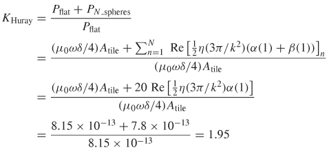
Therefore, the Huray model predicts that the series resistance of a transmission line manufactured according to the roughness profile defined above would be approximately 1.95 times higher than the same transmission line constructed with a smooth conductor at a frequency of 5 GHz.
Figure 5-2 shows a comparison of the insertion losses of a transmission line constructed with rough copper modeled using the Huray equation compared to measured results. Note that the Huray model correctly predicts the shape of the insertion loss curve with less than 1.5 dB of error at 30 GHz. Simulations show that if 23 spheres are used in this example, the model fits the measured results almost exactly [Olufemi, 2007]. However, aside from detailed statistical analysis of the SEM photographs, there is no known deterministic methodology to arrive at the perfect fit. The methodology presented allows the use of a profilometer and produces reasonable wideband results.
Figure 5-26 shows the Huray equation (5-65) constructed with twenty 0.8-µm spheres as calculated in Example 5-5, compared to the Hammerstad and hemisphere models for the roughness profile assumed in Examples 5-4 and 5-5. Note that the Hammerstad equation saturates at 2, which does not provide enough loss
Figure 5-25 Accuracy of the Huray surface roughness model (5-65) constructed with N = 20 spheres with a radius of a = 0.8 µm, assuming a hemispheroid tooth shape; 7-in. microstrip; sr/tanS = 3.9/0.0073 at 1 GHz; RMS roughness of copper foil µRMS = 5.8 µm, Speaks,RMS = 9.4 µm.

Figure 5-26 Surface roughness correction factors for rough copper; Huray model (5-65), hemisphere model (5-58), and Hammerstad model (5-48); RMS roughness: µRMS = 5.8 µm, Speaks,rms = 9.4 µm.

for rough copper. The hemisphere model overpredicts at middle frequencies and slightly underpredicts at high frequencies. As demonstrated by Figure 5-25, a properly constructed Huray model predicts a realistic correction curve.
The frequency dependence of the skin effect resistance and total inductance using the Huray equation for surface roughness is implemented with (5-66a) and(5-66b). When the skin depth (5) is larger than the conductor thickness, the dc value of the resistance and low-frequency inductance where the skin depth is equal to the conductor thickness should be used:
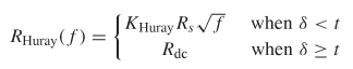

where kHurry is calculated with (5-65), t is the conductor thickness, δ is the skin depth, and fδ=t is the frequency where the skin depth equals the thickness of the conductor.
5.3.4 Conclusions
For rough copper, Figure 5-14b shows that the Hammerstad model slightly overpredicts surface roughness losses at low frequencies and significantly underpredicts losses at high frequencies. However, Figure 5-14a shows that the Hammerstad method works well for copper profiles that are relatively smooth with a corrugated surface profile. The Hammerstad model should be used only for RMS copper roughness profiles less than about 2 µm.
The hemisphere model is an improvement over Hammerstad for rough copper but still overpredicts the losses at middle frequencies and underpredicts the losses at high frequencies, which causes the “belly ”in the simulated results in Figure 5-22. The major benefit gained by studying the hemisphere model is a physical understanding of how the fields and surface currents behave in the presence of a protrusion. The hemisphere is the simplest geometry that can be solved analytically to predict the impact of a rough surface compared to a smooth surface. Furthermore, the hemisphere model is not appropriate for smoother copper profiles that are corrugated in nature. The hemisphere model is valid only for copper profiles that can be characterized by a distribution of distinct protrusions, such as the surfaces shown in Figures 5-16b and 5-23.
The Huray approach is the most diverse and accurate modeling methodology for surface roughness. It can be used for any type of copper as long as a detailed image of the surface profile can be obtained with a profilometer or a scanning electron microscope. The surface area of the roughness profile prior to lamination must be determined, and the number of appropriately sized spheres less than 1µmin radius must be calculated so that the total surface area is equal to that of the roughness profile.
5.4 TRANSMISSION-LINE PARAMETERS FOR NONIDEAL CONDUCTORS
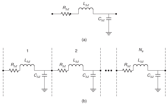
As bus data rates increase and physical implementations of high-speed digital designs shrink, the transmission-line losses become more important. Consequently, the engineer must have the ability to calculate the response of a transmission line successfully and account for realistic conductor behavior. The next two sections will (1) describe how to include ac resistance and internal inductance in an equivalent circuit, and (2) modify telegrapher’s equations to comprehend realistic conductors.
5.4.1 Equivalent Circuit, Impedance, and Propagation Constant
In deriving the equivalent circuit for a transmission line in Section 3.2.3, which is shown in Figure 3-9, the conductor was considered to be infinitely conductive, meaning that all the current flows only on the surface because the skin depth δ= 0, as shown by taking the limit of (5-10) :

Furthermore, the assumption of perfect conductors did not allow the calculation of a resistive term or an internal inductance term because there was no field penetration into the conductor. As described in Section 5.1.2, physical conductors manufactured with metals of finite (although good) conductivity behave very similar to perfect conductors except for a small transition region where internal currents exist that are mostly confined to a few skin depths. As described in Sections 5.2.2 and 5.2.3, the skin effect leads directly to frequency-dependent resistance and internal inductance terms that must be comprehended in the equivalent circuit.
Fortunately, the form of the equivalent circuit derived in Section 3.3 is also applicable to a line whose conductors have finite conductivity. To begin this derivation, the series impedance of an ideal transmission line with infinite conductivity is calculated in units of ohms.
(5-67)![]()
The idealized parameters must be modified to include the surface impedance (also known as the internal impedance):
(5-29)![]()
The total inductance was calculated in (5-20):
indicating that the series impedance contribution from the inductance is simply![]() To calculate the total series impedance of a transmission-line segment, the resistive component is added:
To calculate the total series impedance of a transmission-line segment, the resistive component is added:
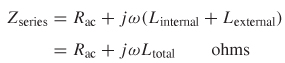
leading to the equivalent circuit for a transmission line with a conductor of finite conductivity, as shown in Figure 5-27, where Ns is the number of segments, ![]() and
and ![]() as calculated in Section 3.2.3, and RΔZ=Δz Rac, where Δz is the length of the differential section of transmission line and C, Ltotal, and Rac are the capacitance, inductance, and resistance per unit length.
as calculated in Section 3.2.3, and RΔZ=Δz Rac, where Δz is the length of the differential section of transmission line and C, Ltotal, and Rac are the capacitance, inductance, and resistance per unit length.
The characteristic impedance, which was defined in equation (3-33), can be calculated by dividing the series impedance as defined by (5-68) by the parallel admittance of the capacitance, Yshunt=jωC for a short section of transmission line of length Δz.
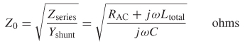
Note that the units in (5-69) are
![]()
Figure 5-27 (a) Model for a differential element of a transmission line; (b) full model.
The propagation constant can be derived by inserting the complex values of the series impedance and shunt admittance into the loss-free formula that was derived in Section 3.2.4, which takes the form
![]()
Substitution of Zseries and Yshunt in place of the loss-free values of the series impedance and the parallel admittance yields the propagation constant for a transmission line with an ideal dielectric and a conductor with a finite conductivity, as shown in
Equations (5-69) and (5-70) account for realistic conductor effects, such as skin effect resistance, internal inductance, and surface roughness, as outlined throughout this chapter.
5.4.2 Telegrapher’s Equations for a Real Conductor and a Perfect Dielectric
The time-harmonic forms of the telegrapher’s equations for a transmission line with a perfect dielectric and perfect conductor were shown in equations (3-25) and (3-26):
(3-25)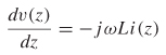
(3-26)![]()
To adjust these formulas to account for a realistic conductor with a finite conductivity, the equivalent circuit must be observed. Notice that the right-hand side of equation (3-25) is simply the impedance of an inductor. Therefore, the series impedance of a differential slice of an ideal transmission line of length dz is based on external inductance since a perfect conductor has infinite conductivity. To account for the realistic conductor effects, the series impedance of a realistic conductor as defined in equation (5-68) is simply substituted into the right hand of (3-25):
(5-71)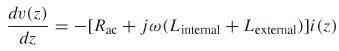
Consequently, the classic form of the telegrapher’s equations for a perfectly insulating dielectric and a realistic conductor are
(5-72a)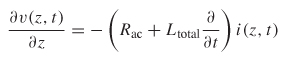
(5-72b)
REFERENCES
Brist, G., S. Hall, S. Clouser, and T. Liang, 2005, Non-classical conductor losses due to copper foil roughness and treatment, CircuiTree, May.
Collins, Robert, 1992, Foundations for Microwave Engineering, McGraw-Hill, New York.
Hall, S., G. Hall, and J. McCall, 2000, High-Speed Digital System Design, Wiley, New York.
Hall, Stephen, Steven G. Pytel, Paul G. Huray, Daniel Hua, Anusha Moonshiram, Gary A. Brist, and Edin Sijercic, 2007, Multi-GHz causal transmission line modeling using a 3-D hemispherical surface roughness approach, IEEE Transactions on Microwave Theory and Techniques, vol. 55, no. 12, Dec.
Hammerstad, E., and O. Jensen, 1980, Accurate models for microstrip computer-aided design, IEEE MTT-S International Microwave Symposium Digest, May, pp. 407-409.
Huray, Paul, 2008, Foundations of Signal Integrity, Wiley, Hoboken, NJ.
Huray, P. G., S. Hall, S. G. Pytel, F. Oluwafemi, R. Mellitz, D. Hua, and P. Ye, 2007, Fundamentals of a 3D “snowball” model for surface roughness power losses, Proceedings of the IEEE Conference on Signals and Propagation on Interconnects, Genoa, Italy, May 14.
Jackson, J. D., 1999, Classical Electrodynamics, 3rd ed., Wiley, New York.
Mathworld, n.d., http://www.mathworld.wolfram.com/ProlateSpheroid.xhtml.
Olufemi, Oluwafemi, 2007, Surface Roughness and Its Impact on System Power Losses, ProQuest, Ann Arbor, MI.
Orlando, Terry P., and Kevin A. Delin, 1991, Foundations of Applied Superconductivity, Addison-Wesley, Reading, MA.
Pytel, Steven G., 2007, Multi-gigabit data signaling rates for PWBs including dielectric losses and effects of surface roughness, Ph.D. dissertation, Department of Electrical Engineering, University of South Carolina.
PROBLEMS
5-1 Draw the resistance, inductance, and impedance curves from 0 to 10 GHz for a microstrip transmission line constructed with copper that has the parameters w = 5 mils, h= 3 mils, t = 2.1 mils, er = 4.1, bbase =10.2 µm, htooth = 4.5 µm, dpeaks= 12 µm, and δ = 5.8 x 10⁸ S/m. Assume a general tooth shape that is hemispheroid in nature. Create the model with the hemisphere model and the Huray model. Discuss the physical mechanisms that cause the differences between the curves.
5-2 Create an equivalent-circuit model valid at 15 GHz of the transmission lines defined in Problem 5-1.
5-3 For the transmission-line description in Problem 5-1, under what condi-tions is the Hammerstad approximation valid?
5-4 For the transmission line defined in Problem 5-1, when do ac losses overtake dc losses?
5-5 What causes internal inductance? Is internal inductance larger or smaller for a thick conductor line versus a thin conductor? What is the relationship between inductance and resistance? In physical terms, explain why the relationship must hold.
5-6 For a stripline transmission line with the parameters w = 5 mils, h1 = h2 = 6 mils (refer to Figure 5-8), t = 0.7 mil, εr = 4.1, bbase = 10.2 µm, htooth = 0.9 µm, and dpeaks = 15 µm, calculate the resistance and inductance at 1 GHz.
5-7 For the transmission-line models defined in Problem 5-1, when do the surface roughness losses become significant?
5-8 For a periodic roughness pattern such as that shown in Figure 5-20, how will the current flow between and on top of the surface protrusions? Assuming TEM fields, draw the magnetic and electric fields and the associated current. What is significant about the periodic pattern? What assumptions break down for a periodic pattern?
5-9 For a 10-in. transmission line with the parameters w = 5 mils, h = 3 mils, t = 2.1 mils, εr = 4.1, and δ = 5.8 x 10⁸S/m, sourced with 5 mA of current, what is the total power per unit area dissipated by the reference plane?
5-10 For the transmission line described in Problem 5-1, how much error would be introduced by neglecting surface roughness at 10 GHz?
5-11 For the transmission line described in Problem 5-1, how much surface roughness would be required to double the power loss of the transmission line?
5-12 For a plane wave impinging onto an infinitely thick slab of a good- conducting medium, draw the electric field outside the conductor and the magnetic fields inside the conductor. Compare and contrast this to the boundary conditions for a perfect conductor.