
9Simulation and Hardware Implementation of Chaotic System
Chaos system can be applied in many fields, such as secure communications, information encryption, system control, system optimization, and so on. To develop the applications of chaos theory, the hardware design and implementation of chaotic systemmust be solved, including the design and implementation of chaotic analog circuit and chaotic digital circuit. In this chapter, we focus on the simulation and hardware implementation of chaotic system.
9.1Dynamic Simulation of Chaotic System
9.1.1Dynamic Simulation Steps on Simulink
Dynamic simulation steps of Simulink are shown in Figure 9.1. The steps include establishing simulation model, setting system parameters and observation window, analyzing simulation results, and modifying model and parameters [188]. A detailed description is presented as follows:
- Establishing simulation mathematical model. It is the key for the simulation of chaos system. According to the chaotic system equation, the whole system is simplified to the source system. Functions of the system are determined, and each part of the function is modeled. We should find out the relationship between the various parts and draw the system flow diagram model. With the increase of the modules and complexity of the system, the model will become more and more complicated. To reduce the number of modules in the model window, we can group the same function modules and simplify the complex problem by packaging subsystem. For example, to observe the time evolution of the synchronization error signal
 the module is constructed as shown in Figure 9.2(a), which can be packaged into a subsystem as shown in Figure 9.2(b), which simplifies the structure of the simulation system.
 - Building simulation system model. According to the established mathematical model, the function module is dragged into the editing window from the Simulink model library. After the modules are connected, the simulation model of chaotic system is constructed.
- Setting simulation parameters. It is an important part of the simulation process, which may directly affect the simulation times and results. Parameters setting include setting operating system parameters (such as the system running time, the integration step size, the tolerable error, the integral algorithm) and the operation parameters of the function modules (such as the initial value, signal amplitude, frequency). The former is finished in the parameter submenu of the Simulink menu, and the latter is finished in the pop-up window by double-clicking the module.


Figure 9.2: Error calculation submodule for synchronization system: (a) error signal function module and (b) packaged subsystem.
4.Setting observation window. The observation module is used to observe the operation of the simulation system, so as to adjust the parameters and analyze the results. The observation modules include the oscilloscope (Scope), XYgraph, Display, to workspace, and so on.
5.Analyzing simulation results and correcting model or parameter. We can judge whether the simulation results are consistent with that of the theoretical analysis by analyzing the output waveform and output data of the simulation system. Generally, it is difficult to succeed at a time. Many factors affect the simulation results. First, you need to check whether the simulation system is consistent with the theoretical model or whether the parameter settings are correct. If the correct simulation results cannot be obtained by checking and modifying the simulation parameters, you need to consider whether the simulation model is correct. We need to modify the model and then simulate it until the results are satisfactory.
9.1.2Simulation Result Analysis and Performance Improvement
Outputting simulation results (graphics) to the word document is an important way to observe the results. First, the output signal is written into the return variable. That is to say, the Out module in the sink library is connected as the output. After choosing the variable time (I/O) and output (Output) box and setting the corresponding time variable tout() and output variable yout(), the simulation is operated. Finally, we can run the Matlab command plot(tout, yout) in the command window. In addition, by using “Figure Copy” in the Edit Windows of the submenu, one can get the copied graph, and then paste it into the drawing software window. To improve the resolution, the graph is generally processed by graphics processing software and then be pasted into the document.
Note that the simulation time is different from the time of simulation running. The simulation time is defined as the difference between the Start time and the Stop time. The time of simulation running is the time to run a simulation. In general, the two are not equal. The time required to run a simulation depends on many factors, including the complexity of the model, the maximum and minimum step size, computer performance, and so on.
Several reasons will lead to simulation time too long. For example, the simulation step size and the tolerance error are too small. When the model contains Fcn Matlab module, the simulation of each step needs to explain the program, which will greatly reduce the simulation speed, so it is best to use the S-function M file. S-function of M file also allows Simulink to call the Matlab interpreter at each simulation time, so it can be replaced by the C-mex function or equivalent subsystem.
9.2Circuit Simulation of Chaotic System
Circuit simulation experiment method is used to simulate the chaotic system by the electronic circuit diagram and to study the characteristics of the chaotic system by analyzing the experimental results. For example, the Electronics Workbench (EWB) software platform is used to design the chaotic system.
EWB is a virtualization working platform that simulates the analog circuit. It has a more perfect model library and several common analytical instruments. It can be used to analyze the electronic circuit and directly output the designed circuit files to common electronic circuit layout software, such as Protel. The experimental analysis steps of the chaotic system are shown in Figure 9.3 [188].
- According to the chaotic system, design the EWB simulation circuit of a chaotic system.
- Choose the components in the window of EWB and connect them.
- Determine the component parameters, including the label of the components and its parameter values.

4. Use EWB virtual instrument to observe the experimental results, analyze data, and compare whether the results are consistent with that of the theoretical analysis. Otherwise we should adjust the circuit.
9.3Design of Chaotic Analog Circuit
9.3.1Procedure of Chaotic Circuit Design
There are three kinds of chaotic circuit design methods, such as individual design, modular design, and improved modular design. The advantage of the individual design is that the number of circuit components is the least, but it needs a rich prior knowledge and circuit design skills. The modular design is based on the nondimensional state equation, which is universal but needs more components. The improved modular design is applied to determine the system parameters by comparing the state differential equation with the actual circuit state differential equation so that the number of components is the minimum. Chaotic circuit modular design flowchart is shown in Figure 9.4. First, based on the dimensionless chaotic state equation, the phase diagrams are calculated to determine the range of the state variables. If the variable is too large to beyond the scope of the dynamic variables of components, the proportion of compression transform is needed, and all variables will be reduced N times. If the variables are within the range, it is not necessary to carry out the compression transformation. Then the EWB circuit simulation is carried out, and the circuit is designed finally.

Circuit design process mainly includes following five steps.
- Variable ratio compression transformation. Because the common power supply voltage is 15 V, the linear dynamic range of an operational amplifier (OA) is 13.5 V. According to the simulation graph, one needs to analyze whether the variable range is beyond. If it is beyond, it needs to do compression transformation.
- Do timescale transformation.
- Do differential integral transformation.
- The equation was standardized to adapt to the inverse phase adder in the module circuit.
- According to the standard integral equation, the corresponding modular circuit is designed.

9.3.2Modular Design of Chaotic Circuit
The modular design of chaotic circuit is designed mainly based on dimensionless equation. The general principle block diagram is shown in Figure 9.5 [196]. The circuit consists of four modules, including nonlinear function, reverse phase additive proportional arithmetic unit, reverse integrator, and inverter. A nonlinear function includes multiplication function, the absolute value function, and so on. Circuits of the latter three modules mainly are built based on amplifiers.
9.3.3Basic Components of Chaotic Circuit
In general, a chaotic circuit contains a nonlinear unit and a linear unit. A nonlinear unit circuit includes analog multiplier, Chua’s diode circuit, the absolute value of the arithmetic circuit and index operation circuit, and so on. Based on the OA device, the common linear basic unit circuits are shown in Figure 9.6, and the input and output expressions of each unit circuit are presented as follows.
- Reverse phase proportion amplifier:
 as shown in Figure 9.6(a).
 - Reverse phase adder:
 as shown in Figure 9.6(b).
 - Subtractor:
 as shown in Figure 9.6(c).
 - Proportional amplifier:
 as shown in Figure 9.6(d).
 - Reverse phase differentiator:
 as shown in Figure 9.6(e).
 - Reverse phase integrator:
 as shown in Figure 9.6(f).

Figure 9.6: Linear unit circuits: (a) reverse phase proportion amplifier; (b) reverse phase adder; (c) subtractor; (d) proportional amplifier; (e) inverse phase differentiator; and (f) reverse phase integrator.
Now taking the simplified Lorenz system as an example, the modular design process is described in detail. The mathematical model of simplified Lorenz system is [56]

where c is the system parameter. When c ∈ [–1.59, 7.75], it is chaotic.
1.When c = 5, by numerical simulation, all the state variables of the system are beyond the dynamic range of the device, so it is necessary to change the system variables. Let x′ = 0.25x, y′ = 0.25y, and z′ = 0.25z, then system (9.1) becomes to

2.Do timescale transformation to system (9.2) and transform t to τ0t′, where τ0 is the time-scaling factor. Let τ0 = 1/(R0C0), then we have

3.After the differential is transformed to integral, the system becomes

4.According to system (9.4), the basic circuit units include inverter, inverting adder, integrator, and multiplier. The circuit is shown in Figure 9.7.
In Figure 9.7, x, y, and z represent the output voltage values, respectively. According to the circuit theory, the state equation of the circuit is obtained:


Figure 9.7: Circuit diagram of simplified Lorenz system.
Comparing eq. (9.4) with eq. (9.5), the value of the components is obtained as Ri = 10 kΩ (i = 1, 2, 4, 5, 6, 11, 12, 13, 17, 18, 19), Ri = 100 kΩ (i = 3,10,16), R7 = 20 kΩ, R8 = 25 kΩ, R9 = R14 = 2.5 kΩ, R15 = 37.5 kΩ, Ci = 100 nF (i = 1, 2, 3).
9.4Improved Modular Design of Chaotic Circuit
The modular design of chaotic circuit is intuitive, simple, and easy to debug, but it has a large number of components. The circuit based on the improved modular design has fewer components, and its precision is higher than that of the standard-type chaotic circuit. The basic unit circuit module is shown in Figure 9.8. Here taking the multiscroll Jerk system as an example, we illustrate the improved modular design in detail.
The equation of multiscroll Jerk system is [197]

where α is the system parameter. When α = 0.6 andf(x) = sgn(x)+sgn(x+2)+sgn(x–2), it can produce a four-scroll chaotic attractor. According to the results of the numerical simulation, the system variables are not beyond the dynamic range of the device, so it is not necessary to do proportion transformation for variables.
Do timescale transformation for system (9.6), let t = τ0t′, τ0 = 10, 000, we obtain

The circuit units for system (9.7) include basic unit circuit module, inverter module, and nonlinear circuit module. Next, we design the system circuit based on OA and current conveyor (CC).

Figure 9.8: General basic unit circuit module based on improved modular design.
9.4.1Design of Multiscroll Jerk Circuit Based on OA
Four-scroll Jerk circuit based on OA devices is shown in Figure 9.9.
In Figure 9.9, x, y, and z represent the output voltage, respectively, the output current value of the subcircuit f(x) is: i(x) = –sgn(x–2)/Rx1–sgn(x)/Rx2–sgn(x+2)/Rx3. According to the circuit theory, we can obtain the state equation of the circuit

Comparing eq. (9.7) with eq. (9.8), the values of the components are obtained as follows: Ri = 10 kΩ (i = 1, 2, 3, 4, 5, 6), Rxi = 135 kΩ (i = 1, 2, 3), R7 = 16.7 kΩ, Ci = 10 nF (i = 1, 2, 3). According to Figure 9.9, we do simulations on EWB, and the results are shown in Figure 9.10.
9.4.2Design of Multiscroll Jerk Circuit Based on CC
The CC is the active device commonly used in current mode circuit, and it has strong versatility, high precision, less external devices, and good high-frequency characteristics. It has been widely used in active power filter, analog signal processing, and so on. Among the CCs, the second-generation current conveyor (CCII) is widely applied. Its circuit symbol is shown in Figure 9.11. Characteristics of the ports are iy = 0, Vx = Vy, and iz = ±ix. When iz = ix, it is the second-generation current conveyor (CCII+). When iz = –ix, it is the reverse second-generation current conveyor (CCII–). CCII+ can be implemented by employing an AD844 device, while CCII– can be realized by cascading two AD844 devices as shown in Figure 9.12.

Figure 9.9: Multiscroll Jerk circuit based on OA devices: (a) main circuit and (b) subcircuit of function f (x).

Figure 9.10: Jerk circuit simulation with four scrolls based on the OA: (a) phase diagram on x–y plane and (b) phase diagram on x–z plane.


Based on CCII+, the common linear basic unit circuits are shown in Figure 9.13; the input and output expressions of each unit circuit are shown as follows [198]:
- Proportional amplifier:
 as shown in Figure 9.13(a).
 - Reverse proportional amplifier:
 as shown in Figure 9.13(b).
 - Inverting differential device:
 as shown in Figure 9.13(c).
 - Inverting adder:
 as shown in Figure 9.13(d).
 - Reverse integrator:
 as shown in Figure 9.13(e).
 - Integrator:
 as shown in Figure 9.13(f).

Figure 9.13: Basic unit circuits: (a) proportional amplifier; (b) reverse proportional amplifier; (c) reverse differentiator; (d) inverting adder; (e) reverse integrator; and (f) integrator.

Figure 9.14: Four-scroll Jerk circuit based on CCII device: (a) main circuit and (b) subcircuit f (x).
Based on the mathematical models and system (9.7), the four-scroll Jerk circuit is designed based on CCII as shown in Figure 9.14.
Nonlinear function f(x) is a step function, and a saturation function is achieved based on the N1 network as shown in Figure 9.14(b). The saturation function sequence is realized by parallel network. If Rb/Ra is large enough, the sequence of saturation function can be approximated by infinite step function. The output current is i(x) = –[sgn(x–2)+sgn(x)+sgn(x+2)]/Rwx. According to the circuit theory, the state equation of the circuit is

Figure 9.15: Four-scroll Jerk chaotic attractor based on CCII: (a) phase diagram on x–y plane and (b) phase diagram on x–z plane.

Figure 9.16: Phase diagram on x–y plane: (a) circuit implement based on OA and (b) circuit implement based on CC.

When comparing eq. (9.7) with eq. (9.9), the value of each component was obtained as follows: Ri = 10 kΩ (i = 1, 2, 3, 4, 6), R5 = 16.7 kΩ, R7 = 20 kΩ, Rwx = 102 kΩ, Ra = 470 Ω, Rb = 1 MΩ, Ci = 10 nF (i = 1, 2, 3). The circuit in Figure 9.14 is simulated on EWB. According to Figure 9.14, we do simulations on EWB, and the results are shown in Figure 9.15.
9.4.3Multiscroll Jerk Circuit Implementation
According to Figures 9.9 and 9.14, the four-scroll Jerk circuit is designed based on CC and OA devices, and the phase diagram is observed by oscilloscope as shown in Figure 9.16. When compared with Figures 9.10 and 9.15, respectively, we concluded that the results of actual circuit experiment and circuit simulation experiment are consistent, and it verified the correctness of the circuit design and the physical realization of the four-scroll Jerk system.
9.5Digital Signal Processor Design and Implementation of Chaotic Systems
Hardware implementation of chaotic system is a key problem for the applications of chaotic system in engineering practice. With the development of microelectronics and digital signal processing technology, the digital circuit realization of chaotic system has become a research hotspot [199–201]. Compared with the analog devices, digital signal processor (DSP) device has the characteristics of stability, repeatability, programmable, and easy to implement. It brings about great developments of digital signal processing in the fields of aviation, aerospace, radar, sonar, communication, domestic appliance, and so on and becomes the core of electronic system. With increase in the calculation speed of DSP, the bandwidth of the real-time processing is greatly increased, and the DSP is widely used in the application of chaotic system.
Here, taking simplified Lorenz system and fractional-order simplified Lorenz system as examples, we will study the DSP implementation of the chaotic system based on DSP TMS320F2812.
9.5.1DSP Experimental Platform of Chaotic System
The hardware platform to implement chaotic system based on DSP is shown in Figure 9.17, in which the D/A converter is the 16-bit dual-channel DAC8552 chip, and the interface chip is MAX3232. Their pin distribution is shown in Figure 9.18.
According to the system requirements, we can choose DSP chip with fixed point or floating point. The main frequency of DSP chip will affect the operation speed, and consequently affect the generating speed of the chaotic sequence. In addition, the width of the data bus will affect the numerical accuracy of the chaotic sequence. We need to consider the DSP chip peripherals to connect with other parts of the system conveniently. Here, we choose TMS320F2812 with 32-bit fixed point DSP chip, amount of peripheral interfaces, and 150 MHz main frequency. Universal Asynchronous Receiver/Transmitter (UART) serial interface is generally used in communication interface, which transmits chaos sequences to the computer in real time. The D/A converter converts the chaotic sequence generated by DSP into analog signals, which can be observed on the oscilloscope. So it demands that the D/A conversion has the dual-channel conversion function for synchronous output, and its conversion speed and precision are high enough. The operation command words of DSP for the DAC8552 are shown in Figure 9.19, where DB15–DB0 is the converted digital signal.

Figure 9.17: Hardware block diagram of chaotic system based on DSP.

By employing CCS4.2 as the DSP integrated development environment, the experimental platform of chaotic system based on DSP is shown in Figure 9.20.
The software flowchart for the realization of the chaos system on DSP is shown in Figure 9.21, which includes DSP initialization, setting of the clock frequency, initialization of the related interface, and so on. Different chaotic system has different system parameters, and the iteration step size, iteration number, and iteration initial value also need to be determined. According to different solution algorithm, we can derive the iterative calculation formula. Each iteration calculation results needs to be stored as the initial value of the next iteration. If data output to D/A or PC, the corresponding data processing is needed, as shown in Figures 9.22 and 9.23.


1.Data processing 1: To realize the D/A conversion correctly, a large enough positive number is added to all of the output value of chaotic sequence, which is equivalent to coordinate translation on the output of the system. DAC8552 is a 16-bit D/A converter, and the converted digital quantity must be positive integers between 0 and 65,535, while the majority value of the chaos sequence generated by DSP is too small. So we need to multiply the sequence value with a positive integer so that the digital numbers are distributed in the whole range of conversion as far as possible.

2.Data processing 2: Similarly, the sequence value of variable is turned to positive. To facilitate the computer display and process, each bit of the chaotic sequence value is converted to ASCII code. Namely, each decimal adds 48 and transmits to the computer bit by bit. Each complete sequence is separated with commas (ASCII 0 × 2C). The length of the data can be chosen. When we analyzing it on computer, the chaotic sequence value can be restored to the values calculated by DSP.
The DSP implementation steps are presented by taking integer-order simplified Lorenz system and its fractional-order counterpart as examples.
9.5.2DSP Implementation of Integer-Order Chaotic System
Taking the simplified Lorenz system as an example, the DSP implementation of the chaotic system based on the fourth-order Runge–Kutta algorithm is described. The simplified Lorenz system equation is [56]

where c is the system parameter. When c ∈ [–1.59, 7.75], it is chaotic. By solving the differential equations based on the fourth-order Runge–Kutta method, we obtain

The recursive parameters are as follows:


where T is the iteration step size. According to eqs (9.11)–(9.15), setting initial values x = 0.1, y = 0.2, z = 0.3, c = 5, and T = 0.01, the attractor phase diagram is generated by the hardware implementation as shown in Figure 9.24.
Taking 4 bits after decimal point of the chaotic sequence generated by DSP, and transmitting a total of 10,000 sequence values between 1,001 and 20,000 to the computer, the phase diagram of the attractor is plotted as shown in Figure 9.25.

Figure 9.24: Attractors in an oscilloscope for the Lorenz system based on the DSP: (a) x–y plane; (b) x–z plane; and (c) y–z plane.

Figure 9.25: Attractors of the simplified Lorenz system by experiment data from DSP: (a) x–y plane; (b) x–z plane; and (c) y–z plane.
9.5.3DSP Implementation of Fractional-Order Chaotic System
Except the difference of the iterative algorithm, the realization of fractional-order chaotic system based on DSP is similar to that of the integer-order chaotic system based on DSP. Fractional-order simplified Lorenz system is described as [186]

where q is the order of fractional differential and c is the system parameter. Choosing suitable q and c, it is chaotic. According to the Adomian decomposition algorithm, the fractional differential equations are solved, and the first seven items are obtained as follows [202]:


For all the above-mentioned equations, h is the iterative step size and Γ(⋅) is the gamma function. According to the calculating process, Γ(⋅) and hnq are unchanged in the iterative process, so to speed up the calculation, we need to calculate the relevant Γ(⋅) and hnq before iteration, taking them as constants in iterative process. The initial values are x0 = 0.1, y0 = 0.2, z0 = 0.3, c = 5, q = 0.9, and h = 0.01, and hardware implementation of the attractor phase diagram is shown in Figure 9.26.
Taking 4 bits after decimal point of the chaotic sequence generated by DSP and transmitting a total of 10,000 sequence values between 10,001 and 20,000 to the computer, the phase diagram of the attractor is plotted as shown in Figure 9.27.
In this chapter, we study the simulation and circuit design techniques of the chaotic system, including the dynamic simulation, circuit simulation, and realization of the chaotic system. The realization of analog circuit and digital circuit of chaotic system has laid an experimental foundation for the applications of chaotic system.
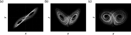
Figure 9.26: Attractors in an oscilloscope for the fractional-order simplified Lorenz system based on the DSP: (a) x–y plane; (b) x–z plane; and (c) y–z plane.

Figure 9.27: Attractors of the fractional-order simplified Lorenz system by experiment data from DSP: (a) x–y plane; (b) x–z plane; and (c) y–z plane.
Questions
- Try to study a chaotic system by using different simulation methods and compare the results.
- What are the similarities and differences of the chaotic systems based on the OA device and the CC device? What is the difference between the chaotic signals generated by them?
- To achieve the digital circuit implementation of a chaotic system, what are the demands for solving algorithm of differential equations?
- Is there finite precision effect in DSP implementation of the chaotic system, and how to overcome it?
- Design and implement a chaotic system circuit.