Chapter Seventeen
Feedback and Flip-Flops
Everybody knows that electricity can make things move. A brief glance around the average home reveals electric motors in appliances as diverse as clocks, fans, food processors, and anything that spins a disk. Electricity also controls the vibrations of loudspeakers, headphones, and earbuds, bringing forth music and speech from our many devices. And even if that’s not an electric car sitting outside, an electric motor is still responsible for starting up antique fossil-fuel engines.
But perhaps the simplest and most elegant way that electricity makes things move is illustrated by a class of devices that are quickly disappearing as electronic counterparts replace them. I refer to those marvelously retro electric buzzers and bells.
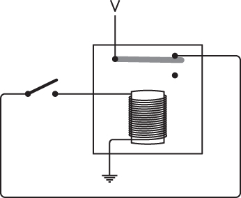
Consider a relay wired like this with a switch and battery:
![]()
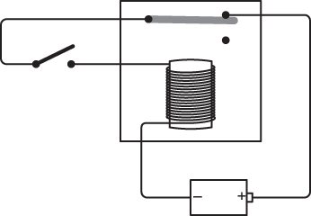
If this looks a little odd to you, you’re not imagining things. We haven’t seen a relay wired quite like this yet. Usually a relay is wired so that the input is separate from the output. Here it’s all one big circle.
If you close the switch, a circuit is completed:
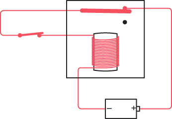
The completed circuit causes the electromagnet to pull down the flexible contact:
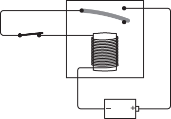
But when the contact changes position, the circuit is no longer complete, so the electromagnet loses its magnetism, and the flexible contact flips back up:

But that completes the circuit again. As long as the switch is closed, the metal contact goes back and forth—alternately closing the circuit and opening it—most likely making a repetitive (and possibly annoying) sound. If the contact makes a rasping sound, it’s a buzzer. If you attach a hammer to it and provide a metal gong, you’ll have the makings of an electric bell.
You can choose from a couple of ways to wire this relay to make a buzzer. Here’s another way to do it using the conventional voltage and ground symbols:
Drawn this way, you might recognize the inverter from Chapter 8 on page 79. The circuit can be drawn more simply this way:
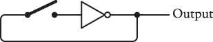
As you’ll recall, the output of an inverter is 1 if the input is 0, and 0 if the input is 1. Closing the switch on this circuit causes the relay or transistor in the inverter to alternately open and close. You can also wire the inverter without a switch so that it goes continuously:

This drawing might seem to be illustrating a logical contradiction because the output of an inverter is supposed to be opposite the input, but here the output is the input! Keep in mind, however, that regardless if the inverter is built from a relay, a vacuum tube, or a transistor, it always requires a little bit of time to change from one state to another. Even if the input is the same as the output, the output will soon change, becoming the inverse of the input, which, of course, changes the input, and so forth and so on.
What is the output of this circuit? Well, the output quickly alternates between providing a voltage and not providing a voltage. Or, we can say, the output quickly alternates between 0 and 1.
This circuit is called an oscillator. It is intrinsically different from anything else you’ve seen so far. All the previous circuits have changed their state only with the intervention of a human being who closes or opens a switch. The oscillator doesn’t require a human being; it basically runs by itself.
Of course, the oscillator in isolation doesn’t seem to be very useful. But we’ll see later in this chapter and in the next few chapters that such a circuit connected to other circuits is an essential part of automation. All computers have some kind of oscillator that makes everything else move in synchronicity. (The oscillators in real computers are somewhat more sophisticated, however, consisting of quartz crystals wired in such a way that they vibrate very consistently and very quickly.)
The output of the oscillator alternates between 0 and 1. A common way to symbolize that fact is with a diagram that looks like this:

This is understood to be a type of graph. The horizontal axis represents time, and the vertical axis indicates whether the output is 0 or 1:
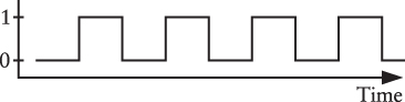
All this is really saying that as time passes, the output of the oscillator alternates between 0 and 1 on a regular basis. For that reason, an oscillator is sometimes referred to as a clock because by counting the number of oscillations you can tell time (kind of).
How fast will the oscillator run? How many times a second will the output alternate between 0 and 1? That obviously depends on how the oscillator is built. One can easily imagine a big, sturdy relay that clunks back and forth slowly and a small, light relay that buzzes rapidly. A transistor oscillator can vibrate millions or billions of times per second.
One cycle of an oscillator is defined as the interval during which the output of the oscillator changes and then comes back again to where it started:
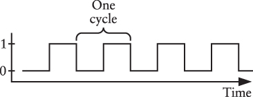
The time required for one cycle is called the period of the oscillator. Let’s assume that we’re looking at a particular oscillator that has a period of 0.02 seconds. The horizontal axis can be labeled in seconds beginning from some arbitrary time denoted as 0:
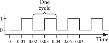
The frequency of the oscillator is 1 divided by the period. In this example, if the period of the oscillator is 0.02 second, the frequency of the oscillator is 1 ÷ 0.02, or 50 cycles per second. Fifty times per second, the output of the oscillator changes and changes back.
Cycles per second is a fairly self-explanatory term, much like miles per hour or pounds per square inch or calories per serving. But cycles per second isn’t used much anymore. In commemoration of Heinrich Rudolph Hertz (1857–1894), who was the first person to transmit and receive radio waves, the word hertz is now used instead. This usage started first in Germany in the 1920s and then expanded into other countries over the decades.
Thus, we can say that our oscillator has a frequency of 50 hertz, or (to abbreviate) 50 Hz.
Of course, we just guessed at the actual speed of one particular oscillator. By the end of this chapter, we’ll be able to build something that lets us actually measure the oscillator’s speed.
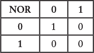
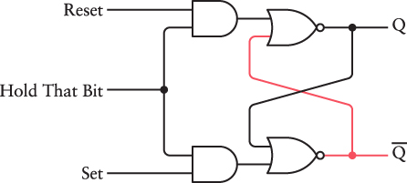
To begin this endeavor, let’s look at a pair of NOR gates wired in a particular way. You’ll recall that the output of a NOR gate is a voltage only if both inputs aren’t voltages:
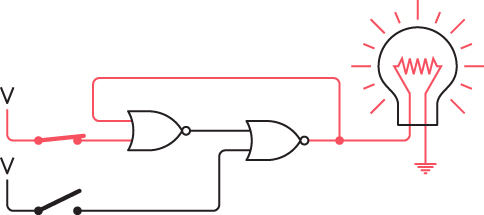
Here’s a circuit with two NOR gates, two switches, and a lightbulb:
![]()

Notice the oddly contorted wiring: The output of the NOR gate on the left is an input to the NOR gate on the right, and the output of that NOR gate is an input to the first NOR gate. This is a type of feedback. Indeed, just as in the oscillator, an output circles back to become an input. This idiosyncrasy will be characteristic of most of the circuits in this chapter.
There’s a simple rule in using this circuit: You can close either the top switch or the bottom switch, but not both switches at the same time. The following discussion is dependent on that rule.
At the outset, the only current flowing in this circuit is from the output of the left NOR gate. That’s because both inputs to that gate are 0. Now close the upper switch. The output from the left NOR gate becomes 0, which means the output from the right NOR gate becomes 1 and the lightbulb goes on:
The magic occurs when you now open the upper switch. Because the output of a NOR gate is 0 if either input is 1, the output of the left NOR gate remains the same and the light remains lit:
Now this is odd, wouldn’t you say? Both switches are open—the same as in the first drawing—yet now the lightbulb is on. This situation is certainly different from anything we’ve seen before. Usually the output of a circuit is dependent solely upon the inputs. That doesn’t seem to be the case here. Moreover, at this point you can close and open that upper switch and the light remains lit. That switch has no further effect on the circuit because the output of the left NOR gate remains 0.
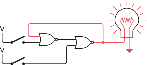
Now close the lower switch. Because one of the inputs to the right NOR gate is now 1, the output becomes 0 and the lightbulb goes out. The output of the left NOR gate becomes 1:
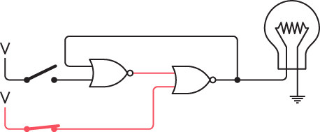
Now you can open the bottom switch and the lightbulb stays off:
We’re back where we started. At this time, you can close and open the bottom switch with no further effect on the lightbulb. In summary:
Closing the top switch causes the lightbulb to go on, and it stays on when the top switch is opened.
Closing the bottom switch causes the lightbulb to go off, and it stays off when the bottom switch is opened.
The strangeness of this circuit is that sometimes when both switches are open, the light is on, and sometimes when both switches are open, the light is off. We can say that this circuit has two stable states when both switches are open. Such a circuit is called a flip-flop, a word also used for beach sandals and the tactics of politicians. The flip-flop dates from 1918 with the work of English radio physicists William Henry Eccles (1875–1966) and F.W. Jordan (1881–1941). A flip-flop circuit retains information. It “remembers.” It only remembers what switch was most recently closed, but that is significant. If you happen to come upon such a flip-flop in your travels and you see that the light is on, you can surmise that it was the upper switch that was most recently closed; if the light is off, the lower switch was most recently closed.
A flip-flop is very much like a seesaw. A seesaw has two stable states, never staying long in that precarious middle position. You can always tell from looking at a seesaw which side was pushed down most recently.
Although it might not be apparent yet, flip-flops are essential tools. They add memory to a circuit to give it a history of what’s gone on before. Imagine trying to count if you couldn’t remember anything. You wouldn’t know what number you were up to and what number comes next! Similarly, a circuit that counts (which I’ll show you later in this chapter) needs flip-flops.
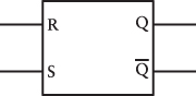
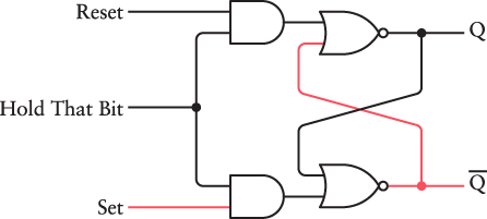
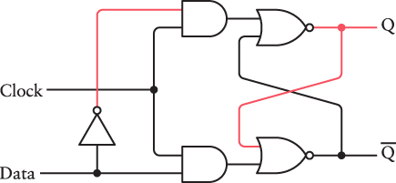
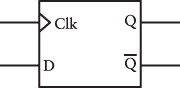
Flip-flops are found in a couple of different varieties. What you’ve just seen is the simplest and is called an R-S (or Reset-Set) flip-flop. The two NOR gates are more commonly drawn and labeled as in the following diagram to give it a symmetrical look:
![]()
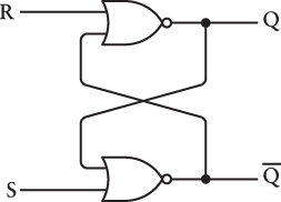
The output that we used for the lightbulb is traditionally called Q. In addition, there’s a second output called Q (pronounced Q bar) that’s the opposite of Q. If Q is 0, then Q is 1, and vice versa. The two inputs are called S for set and R for reset. You can think of these verbs as meaning “set Q to 1” and “reset Q to 0.” When S is 1 (which corresponds to closing the top switch in the earlier diagram), Q becomes 1, and Q becomes 0. When R is 1 (corresponding to closing the bottom switch in the earlier diagram), Q becomes 0, and Q becomes 1. When both inputs are 0, the output indicates whether Q was last set or reset. These results are summed up in the following table:
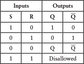
This is called a function table or a logic table or a truth table. It shows the outputs that result from particular combinations of inputs. Because there are only two inputs to the R-S flip-flop, the number of combinations of inputs is four. These correspond to the four rows of the table under the headings.
Notice the row second from the bottom when S and R are both 0: The outputs are indicated as Q and Q. This means that the Q and Q outputs remain what they were before both the S and R inputs became 0. The final row of the table indicates that making both the S and R inputs 1 is disallowed or illegal. This doesn’t mean you’ll get arrested for doing it, but if both inputs are 1 in this circuit, both outputs are 0, which violates the notion of Q being the opposite of Q. If you’re designing circuitry that uses the R-S flip-flop, you’ll want to avoid situations in which the S and R inputs are both 1.
The R-S flip-flop is often drawn as a little box with the two inputs and two outputs labeled like this:
The R-S flip-flop is certainly interesting as a first example of a circuit that seems to “remember” which of two inputs was last a voltage. What turns out to be much more useful, however, is a circuit that remembers whether a particular signal was 0 or 1 at a particular point in time.
Let’s think about how such a circuit should behave before we actually try to build it. It would have two inputs. Let’s call one of them Data. Like all digital signals, the Data input can be 0 or 1. Let’s call the other input Hold That Bit, which is the digital equivalent of a person saying “Hold that thought.” Normally the Hold That Bit signal is 0, in which case the Data signal has no effect on the circuit. When Hold That Bit is 1, the circuit reflects the value of the Data signal. The Hold That Bit signal can then go back to being 0, at which time the circuit remembers the last value of the Data signal. Any changes in the Data signal have no further effect.
In other words, we want something that has the following function table:
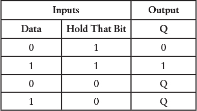
In the first two cases, when the Hold That Bit signal is 1, the Q output is the same as the Data input. In the second two cases, when the Hold That Bit signal is 0, the Q output is the same as it was before regardless of what the Data input is. The function table can be simplified a little, like this:
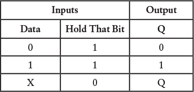
The X means “don’t care.” It doesn’t matter what the Data input is because if the Hold That Bit input is 0, the Q output is the same as it was before.
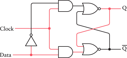
Implementing a Hold That Bit signal based on the existing R-S flip-flop requires that we add two AND gates at the input end, as in the following diagram:
![]()
I know this doesn’t include a Data input, but I’ll fix that shortly.
Recall that the output of an AND gate is 1 only if both inputs are 1, which means that the Reset and Set inputs have no effect on the rest of the circuit unless Hold That Bit is 1.
The circuit starts out with a value of Q and an opposite value of Q. In this diagram, the Q output is 0, and the Q output is 1. As long as the Hold That Bit signal is 0, the Set signal has no effect on the outputs:
Similarly, the Reset signal has no effect:
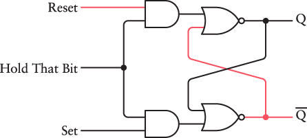
Only when the Hold That Bit signal is 1 will this circuit function the same way as the normal R-S flip-flop shown earlier:
It behaves like a normal R-S flip-flop because now the output of the upper AND gate is the same as the Reset signal, and the output of the lower AND gate is the same as the Set signal.
But we haven’t yet achieved our goal. We want only two inputs, not three. How is this done?
If you recall the original function table of the R-S flip-flop, the case in which Set and Reset were both 1 was disallowed, so we want to avoid that. And it also doesn’t make much sense for the Set and Reset signals to both be 0 because that’s simply the case in which the output doesn’t change. We can accomplish the same thing in this circuit by setting Hold That Bit to 0. This implies that it only makes sense for Set and Reset to be opposite each other: If Set is 1, Reset is 0; and if Set is 0, Reset is 1.
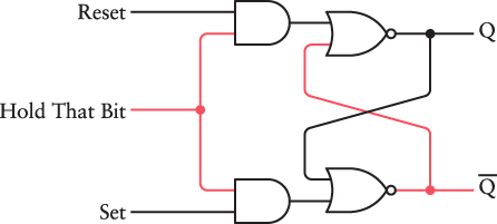
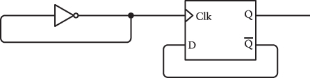
Let’s make two changes to the circuit. The Set and Reset inputs can be replaced with a single Data input. This is equivalent to the previous Set input. That Data signal can be inverted to replace the Reset signal.
The second change is to give the Hold That Bit signal a more traditional name, which is Clock. This might seem a little odd because it’s not a real clock, but you’ll see shortly that it might sometimes have clocklike attributes, which means that it might tick back and forth between 0 and 1 on a regular basis. But for now, the Clock input simply indicates when the Data input is to be saved.
Here’s the revised circuit. The Data input replaces the Set input on the bottom AND gate, while an inverter inverts that signal to replace the Reset input on the top AND gate:
![]()
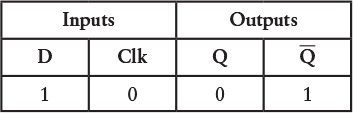
Again, we begin with both inputs set to 0. The Q output is 0, which means that Q is 1. As long as the Clock input is 0, the Data input has no effect on the circuit:
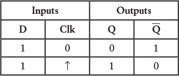
But when Clock becomes 1, the circuit reflects the value of the Data input:
The Q output is now the same as the Data input, and Q is the opposite. Now Clock can go back to being 0:
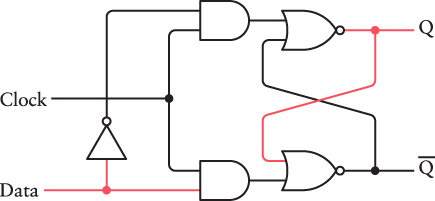
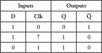
The circuit now remembers the value of Data when Clock was last 1, regardless of how Data changes. The Data signal could, for example, go back to 0 with no effect on the output:
This circuit is called a level-triggered D-type flip-flop. The D stands for Data. Level-triggered means that the flip-flop saves the value of the Data input when the Clock input is at a particular level, in this case 1. (We’ll look at an alternative to level-triggered flip-flops shortly.)
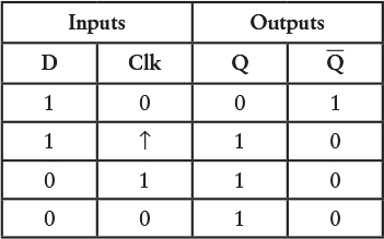
In the function table, Data can be abbreviated as D and Clock as Clk:
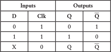
This circuit is also known as a level-triggered D-type latch, and that term simply means that the circuit latches onto one bit of data and keeps it around for further use. The circuit can also be referred to as a 1-bit memory. I’ll demonstrate in Chapter 19 how very many of these flip-flops can be wired together to provide many bits and bytes of memory.
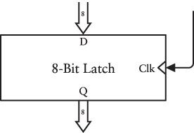
For now, let’s try saving just 1 byte of data. You can assemble eight level-triggered D-type flip-flops with all the Clock inputs consolidated into one signal. Here’s the resultant package:
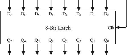
This latch is capable of saving a whole byte at once. The eight inputs on the top are labeled D0 through D7 , and the eight outputs on the bottom are labeled Q0 through Q7. The input at the right is the Clock. The Clock signal is normally 0. When the Clock signal is 1, the entire 8-bit value on the D inputs is transferred to the Q outputs. When the Clock signal goes back to 0, that 8-bit value stays there until the next time the Clock signal is 1. The Q outputs from each latch are ignored.
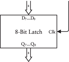
The 8-bit latch can also be drawn with the eight Data inputs and eight Q outputs grouped together in a data path, as shown here:
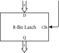
Or simplified even more with the inputs labeled simply D and Q:
Toward the end of Chapter 14, eight 1-bit adders were also collected and wired together to add entire bytes:
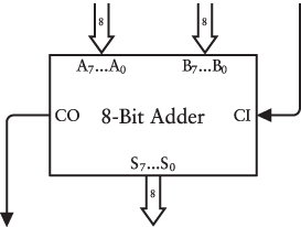
In that chapter, the eight A inputs and eight B inputs were connected to switches, the CI (Carry In) input was connected to ground, and the eight S (Sum) outputs and CO (Carry Out) outputs were wired to lightbulbs.
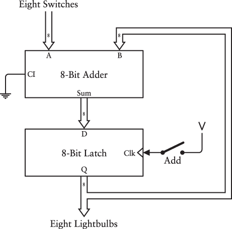
The latch and adder can be used as modular building blocks in assembling more complex circuitry. For example, it’s possible to save the output of the 8-bit adder in an 8-bit latch. It’s also possible to replace one of the rows of eight switches with an 8-bit latch so that the output of the latch is an input to the adder. Here’s something that combines those two concepts to make what might be called an “accumulating adder” that keeps a running total of multiple numbers:
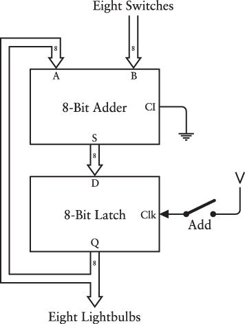
Notice that the switch labeled Add controls the Clock input of the latch.
Besides reducing the number of switches by half, this configuration allows you to add more than just two numbers without re-entering intermediate results. The output of the latch begins with an output of all zeros, which is also the A input to the adder. You key in the first number and toggle the Add button—close the switch and then open it. That number is stored by the latch and appears on the lights. You then key in the second number and again toggle the Add button. The number set up by the switches is added to the previous total, and it appears on the lights. Just continue keying in more numbers and toggling the Add switch.
Unfortunately, it doesn’t quite work how you would hope. It might work if you built the adder from slow relays and you were able to flip the Add switch very quickly to store the result of the adder in the latch. But when that Add switch is closed, any change to the Data inputs of the latch will go right through to the Q outputs and then back up to the adder, where the value will be added to the switches, and the sum will go back into the latch and circle around again.
This is what’s called an “infinite loop.” It occurs because the D-type flip-flop we designed was level-triggered. The Clock input must change its level from 0 to 1 in order for the value of the Data input to be stored in the latch. But during the time that the Clock input is 1, the Data input can change, and those changes will be reflected in the values of the outputs.
For some applications, a level-triggered Clock input is quite sufficient. But for the accumulating adder, it just doesn’t work. For the accumulating adder, we don’t want a latch that allows the data to flow through whenever the Clock input is 1. Much preferred would be a latch that saves the data at the very instant the Clock changes from 0 to 1 (or alternatively from 1 to 0). This transition is called an edge because that’s what it looks like graphically:

The transition from 0 to 1 is sometimes called a positive transition or a positive edge, and the transition from 1 to 0 is a negative transition or negative edge.
The level-triggered flip-flop shown earlier latched the data when the Clock input is 1. In contrast, a positive edge-triggered flip-flop latches the data only when the Clock makes a transition from 0 to 1. As with the level-triggered flip-flop, when the Clock input is 0, any changes to the Data input don’t affect the outputs. The difference in a positive edge-triggered flip-flop is that changes to the Data input also don’t affect the outputs when the Clock input is 1. The Data input affects the outputs only at the instant that the Clock changes from 0 to 1.
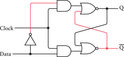
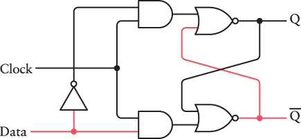
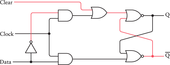
This concept is unlike anything encountered so far, so it might seem difficult to implement. But there’s a trick involved: An edge-triggered D-type flip-flop is constructed from two stages of level-triggered D-type flip-flops, wired together this way:
![]()
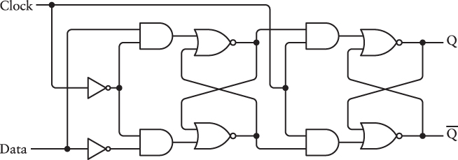
The idea here is that the Clock input controls both the first stage and the second stage. But notice that the clock is inverted in the first stage. This means that the first stage works exactly like a D-type flip-flop except that the Data input is stored when the Clock is 0. The outputs of the first stage are inputs to the second stage, and these are saved when the Clock is 1. The overall result is that the Data input is saved only when the Clock changes from 0 to 1.
Let’s take a closer look. Here’s the flip-flop at rest with both the Data and Clock inputs at 0 and the Q output at 0:
Now change the Data input to 1:
This changes the first flip-flop stage because the inverted Clock input is 1. But the second stage remains unchanged because the uninverted Clock input is 0. Now change the Clock input to 1:
This causes the second stage to change, and the Q output goes to 1. The difference is that the Data input can now change (for example, back to 0) without affecting the Q output:
The Q and Q outputs can change only at the instant that the Clock input changes from 0 to 1.
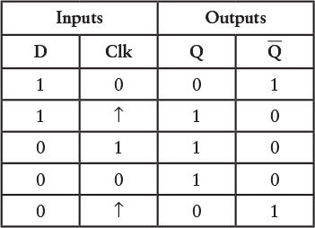
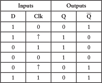
The function table of the edge-triggered D-type flip-flop requires a new symbol, which is an arrow pointing up (↑). This symbol indicates a signal making a transition from a 0 to a 1:
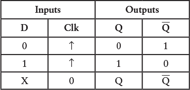
The arrow pointing up indicates that the Q output becomes the same as the Data input when the Clock makes a positive transition, which is a transition from 0 to 1. The flip-flop has a diagram like this:
The little angle bracket on the Clk input indicates that the flip-flop is edge triggered. Similarly, a new assemblage of eight edge-triggered flip-flops can be symbolized with a little bracket on the Clock input:
This edge-triggered latch is ideal for the accumulating adder:
![]()
This accumulating adder is not handling the Carry Out signal very well. If the addition of two numbers exceeds 255, the Carry Out is just ignored, and the lightbulbs will show a sum less than what it should be. One possible solution is to make the adder and latch all 16 bits wide, or at least wider than the largest sum you’ll encounter. But let’s hold off on solving that problem.
Another issue is that there’s no way to clear this adder to begin a new running total. But there is an indirect way to do it. In the previous chapter you learned about ones’ complement and two’s complement, and you can use those concepts: If the running total is 10110001, for example, enter the ones’ complement (01001110) on the switches and add. That total will be 11111111. Now enter just 00000001 on the switches and add again. Now all the lightbulbs will be off, and the adder is cleared.
Let’s now explore another type of circuit using the edge-triggered D-type flip-flop. You’ll recall the oscillator constructed at the beginning of this chapter. The output of the oscillator alternates between 0 and 1:
Let’s connect the output of the oscillator to the Clock input of the edge-triggered D-type flip-flop. And let’s connect the Q output to the D input:
The output of the flip-flop is itself an input to the flip-flop. It’s feedback upon feedback! (In practice, this could present a problem. The oscillator is constructed out of a relay or other switching component that’s flipping back and forth as fast as it can. The output of the oscillator is connected to the components that make up the flip-flop. These other components might not be able to keep up with the speed of the oscillator. To avoid these problems, let’s assume that the oscillator is much slower than the flip-flops used elsewhere in these circuits.)
To see what happens in this circuit, let’s look at a function table that illustrates the various changes. It’s a little tricky, so let’s take it step by step. Begin with the Clock input at 0 and the Q output at 0. That means that the Q output is 1, which is connected to the D input:
When the Clock input changes from 0 to 1, the Q output will become the same as the D input:
The Clock input is now 1. But because the Q output changes to 0, the D input will also change to 0:
The Clock input changes back to 0 without affecting the outputs:
Now the Clock input changes to 1 again. Because the D input is 0, the Q output becomes 0, and the Q output becomes 1:
So the D input also becomes 1:
What’s happening here can be summed up very simply: Every time the Clock input changes from 0 to 1, the Q output changes, either from 0 to 1 or from 1 to 0. The situation is clearer if we look at the timing diagram:
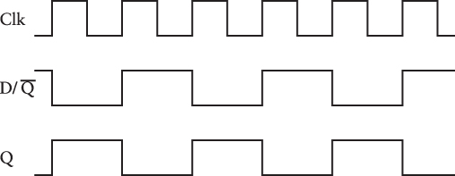
When the Clock input goes from 0 to 1, the value of D (which is the same as Q) is transferred to Q, thus also changing Q and D for the next transition of the Clock input from 0 to 1.
Earlier I mentioned that the rate at which a signal oscillates between 0 and 1 is called the frequency and is measured in Hertz (and abbreviated Hz), which is equivalent to cycles per second. If the frequency of the oscillator is 20 Hz (which means 20 cycles per second), the frequency of the Q output is half that, or 10 Hz. For this reason, such a circuit—in which the Q output is routed back to the Data input of a flip-flop—is also known as a frequency divider.
Of course, the output from the frequency divider can be the Clock input of another frequency divider to divide the frequency once again. Here’s an arrangement of just three of these cascading flip-flops, but the row could be extended:
![]()
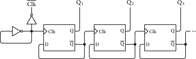
Let’s look at the four signals I’ve labeled at the top of that diagram:
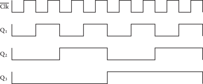
I’ll admit that I’ve started and ended this diagram at an opportune spot, but there’s nothing dishonest about it: The circuit will repeat this pattern over and over again. But do you recognize anything familiar about it?
I’ll give you a hint. Let’s label these signals with 0s and 1s:
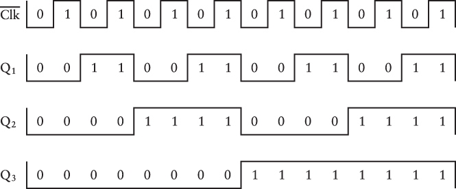
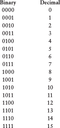
Do you see it yet? Try turning the diagram 90 degrees clockwise, and read the 4-bit numbers going across. Each of them corresponds to a decimal number from 0 through 15:
Thus, this circuit is doing nothing less than counting in binary numbers, and the more flip-flops we add to the circuit, the higher it will count. I pointed out in Chapter 10 that in a sequence of increasing binary numbers, each column of digits alternates between 0 and 1 at half the frequency of the column to the right. The counter mimics this. At each positive transition of the Clock signal, the outputs of the counter are said to increment—that is, to increase by 1.
Let’s string eight flip-flops together and put them in a box:
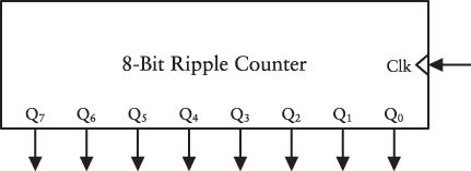
This is called a ripple counter because the output of each flip-flop becomes the Clock input of the next flip-flop. Changes ripple through the stages sequentially, and the flip-flops at the end might be delayed a little in changing. More sophisticated counters are synchronous, which means that all the outputs change at the same time.
I’ve labeled the outputs Q0 through Q7. These are arranged so that the output from the first flip-flop in the chain (Q0) is at the far right. Thus, if you connected lightbulbs to these outputs, you could read an 8-bit number.
I mentioned earlier in this chapter that we’d discover some way to determine the frequency of an oscillator. This is it. If you connect an oscillator to the Clock input of the 8-bit counter, the counter will show you how many cycles the oscillator has gone through. When the total reaches 11111111 (255 in decimal), it goes back to 00000000. (This is sometimes known as rollover or wraparound.) Probably the easiest way to determine the frequency of an oscillator is to connect eight lightbulbs to the outputs of this 8-bit counter. Now wait until all the outputs are 0 (that is, when none of the lightbulbs are lit) and start a stopwatch. Stop the stopwatch when all the lights go out again. That’s the time required for 256 cycles of the oscillator. Say it’s 10 seconds. The frequency of the oscillator is thus 256 ÷ 10, or 25.6 Hz.
In real life, oscillators built from vibrating crystals are much faster than this, starting on the low end at 32,000 Hz (or 32 kilohertz or kHz), up to a million cycles per second (a megahertz or MHz) and beyond, and even reaching a billion cycles per second (a gigahertz or GHz).
One common type of crystal oscillator has a frequency of 32,768 Hz. This is not an arbitrary number! When that is an input to a series of frequency dividers, it becomes 16,384 Hz, then 8192 Hz, 4096 Hz, 2048 Hz, 1024 Hz, 512 Hz, 256 Hz, 128 Hz, 64 Hz, 32 Hz, 16 Hz, 8 Hz, 4 Hz, 2 Hz, and 1 Hz, at which point it can count seconds in a digital clock.
One practical problem with ripple counters is that they don’t always start at zero. When power comes on, the Q outputs of some of the individual flip-flops might be 1 or might be 0. One common enhancement to flip-flops is a Clear signal to set the Q output to 0 regardless of the Clock and Data inputs.
For the simpler level-triggered D-type flip-flop, adding a Clear input is fairly easy and requires only the addition of an OR gate. The Clear input is normally 0. But when it’s 1, the Q output becomes 0, as shown here:
![]()
This signal forces Q to be 0 regardless of the other input signals, in effect clearing the flip-flop.
For the edge-triggered flip-flop, the Clear signal is more complex, and if we’re going to add a Clear signal, we might also consider adding a Preset signal as well. While the Clear signal sets the Q output to 0 regardless of the Clock and Data inputs, the Preset sets Q to 1. If you were building a digital clock, these Clear and Preset signals would be useful for setting the clock to an initial time.
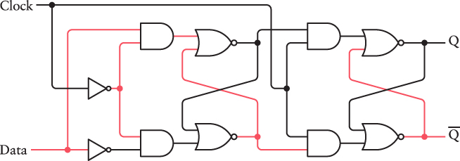
Here’s the edge-triggered D-type flip-flop with preset and clear built entirely from six 3-input NOR gates and an inverter. What it lacks in simplicity it makes up in symmetry:
![]()
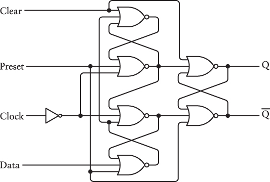
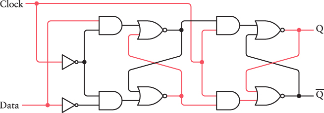
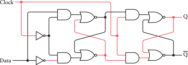
The Preset and Clear inputs override the Clock and Data inputs. Normally these Preset and Clear inputs are both 0. When the Preset input is 1, Q becomes 1, and Q becomes 0. When the Clear input is 1, Q becomes 0, and Q becomes 1. (Like the Set and Reset inputs of an R-S flip-flop, Preset and Clear shouldn’t be 1 at the same time.) Otherwise, this behaves like a normal edge-triggered D-type flip-flop:
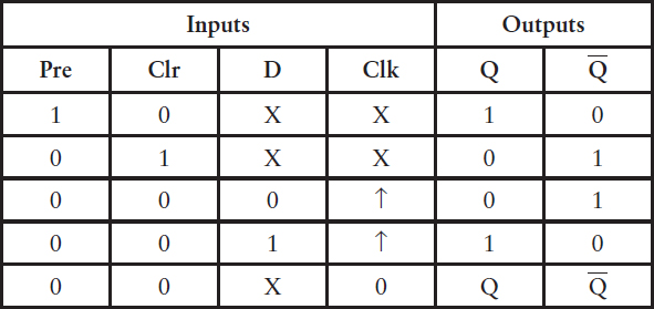
The diagram for the edge-triggered D-type flip-flop with preset and clear looks like this:
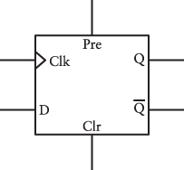
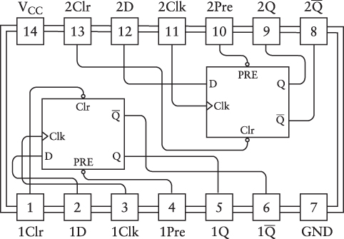
In Chapter 15, I described some examples of integrated circuits in the family known as TTL (transistor-transistor logic). If you were working with TTL and you needed one of these flip-flops, you don’t need to build it from gates. The 7474 chip is described as a “Dual D-Type Positive-Edge-Triggered Flip-Flop with Preset and Clear,” and here’s how it’s shown in the TTL Data Book for Design Engineers:
We have now persuaded telegraph relays and transistors to add, subtract, and count in binary numbers. We’ve also seen how flip-flops can store bits and bytes. This is the first step to constructing an essential component of computers known as memory.
But let’s first have some fun.