Chapter Twenty-Two
Registers and Busses
Many of the routine operations of a computer involve moving stuff around, and by “stuff” I mean bytes of course. We experience this movement of bytes every time we load or save a file, when streaming music or movies, or when videoconferencing. Sometimes if those bytes don’t move fast enough, sound or video can freeze or become garbled. We’ve all been there.
On a more micro level, bytes also move within the central processing unit (CPU) itself. Bytes move from memory into the CPU, and into the arithmetic logic unit (ALU). Results from the ALU sometimes go back into the ALU for additional arithmetic or logical operations before eventually being moved into memory.
This movement of bytes within the CPU is not quite as glamorous as the number crunching of the ALU, but it is just as essential.
As these bytes are moved within the CPU, they are stored in a collection of latches. This is a concept that should be familiar from the Triple-Byte Accumulator in Chapter 20. That machine contained four 8-bit latches, one for storing an instruction code and the other three for storing data bytes.
The CPU that I’m building in these chapters is based on the Intel 8080 microprocessor, and it will require more than just four latches. I won’t show you all of them right away. I first want to focus on seven very special 8-bit latches that can be directly controlled by CPU instructions. These latches are called registers, and a primary purpose of these registers is to store bytes as they are processed by the ALU.
All seven of these registers are important, but one of them is especially important, and that one is called the accumulator.
How special is the accumulator? As you’ll recall from the previous chapter, the ALU has two inputs labeled A and B. In the Intel 8080 (and hence, the CPU that I’m building), the first of these two inputs is always the value stored in the accumulator, and the output of the ALU is always stored back in the accumulator. From the accumulator, it can be moved to one of the other registers or stored in memory.
The seven registers are identified by letters. The accumulator is also known as register A. Four of the other registers are unimaginatively labeled B, C, D, and E. But the final two registers are not F and G. As you’ll see, these two registers are often used together to create a 16-bit address for accessing memory. For that reason, they are called H and L, standing for “high byte” and “low byte.”
In summary, the Intel 8080 (and my CPU) defines seven registers referred to as A, B, C, D, E, H, and L.
On page 318 in the previous chapter, I identified the operation code 3Eh as the “Code to move next byte into CPU.” More precisely, that is the code to move the next byte in memory into the accumulator, also known as register A. That code 3Eh is part of a family of similar codes implemented by the 8080:
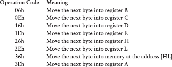
Code 3Eh is at the bottom of this table. Yes, it’s true that the numerical order of these codes does not match the alphabetical order of the registers, but that’s just the way it is.
Notice code 36h. This code is different from the others in the table. It doesn’t move the byte following the operation code into one of the seven latches. Instead, that byte is stored in memory at the 16-bit memory address formed by the H and L registers, which is symbolized as [HL].
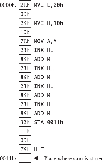
I haven’t yet completed building a CPU that understands these instructions, but if we had such a CPU (or a computer using an Intel 8080), we could run the following little computer program that uses three of these instruction codes:
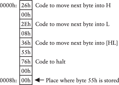
Three of these codes—26h, 2Eh, and 36h—are in the table I just showed you. The first moves the next byte in memory (which is 00h) into register H. The second moves the byte 08h into register L. The registers H and L together now form the memory address 0008h. The third instruction code is 36h, which means to store the next byte (which is 55h) into memory at [HL], which is the address formed by the H and L registers. Finally, the code 76h is encountered, which halts the CPU.
The use of registers H and L to form a 16-bit memory address is known as indirect addressing, and while it might not be obvious at the moment, it turns out to be very useful.
If you examine the bits in the eight operation codes in the previous table, you’ll discover a pattern. All these eight codes are made up of these bits:
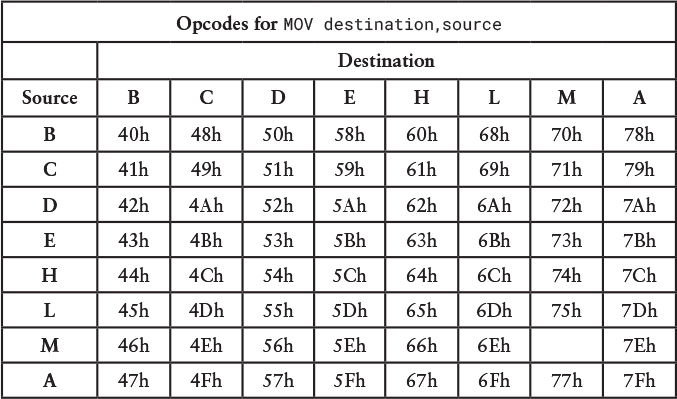
where DDD is a 3-bit code for the destination of the byte, as shown in the following table:
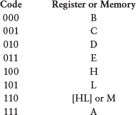
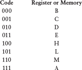
Code 110 in this table indicates a memory location addressed by the 16-bit combination of registers H and L. I personally prefer to denote that memory location as [HL], but Intel’s documentation of the 8080 refers to it as M (standing for memory, of course) as if M were simply another register.
If all the operation codes supported by an 8-bit processor are 1 byte in length, how many operation codes can there be? Obviously 256. It turns out that the Intel 8080 only defines 244 instruction codes, leaving 12 8-bit values undefined. So far, you’ve seen two tables of eight instruction codes each, the first in Chapter 21 on page 329, and eight more in the table on page 336. On page 318 in Chapter 21, you were also introduced to codes 32h, which stores a byte in a memory address that follows the instruction code, and 76h, which halts the processor.
Hold on to your hat, because the next table contains 64 operation codes:

This table contains more than a quarter of all the operation codes implemented by the Intel 8080. These operations constitute the core of the arithmetical and logical functions supported by the CPU.
At the top of the eight columns of operation codes you’ll see three-letter abbreviations for Add, Add with Carry, Subtract, and Subtract with Borrow; the logical operations AND, XOR, and OR; and Compare. These are the abbreviations that Intel uses in its documentation of the 8080 microprocessor. You can think of them as mnemonics—that is, simple words to help you remember longer operations—but they also play an important role when writing programs for the 8080.
Each of the eight arithmetic and logical operations can be combined with a source shown in the leftmost column, which lists the seven registers and memory accessed by [HL].
These abbreviations provide convenient ways to refer to the instruction codes. For example, instead of saying “code to add the content of register E to the accumulator” or “operation code 83h,” you can simply say:
ADD E
The sum of register E and the accumulator is stored back in the accumulator.
Instead of saying “Perform an exclusive OR operation between the accumulator and the memory byte stored at [HL]” or “operation code AEh,” you can simply say:
XRA M
The result is stored back in the accumulator.
These abbreviations are formally known as assembly language instructions. The term originated in the early 1950s and refers to the process of assembling a computer program. The mnemonics are a very concise way of referring to a particular instruction code implemented by the CPU. The assembly language instruction XRA M is the same as the operation code AEh, and vice versa.
All 64 instructions in the previous table have the following bit patterns:
where FFF is the code for the arithmetic or logical function as implemented in the ALU in Chapter 21. The code SSS refers to the source register or memory, which are the same codes as in the table on page 337.
Earlier, on page 336, you saw a table of instruction codes that moved the byte following the instruction code into one of the registers or memory. These are referred to as move immediate instructions, which is abbreviated MVI. Now it’s time to stop referring to them with English descriptions and begin using the official assembly language instructions:

I’ve also moved the operation code to the last column to emphasize the primacy of the assembly language instruction. The word data refers to the byte following the operation code.
The code 32h introduced on page 318 of Chapter 21 stores the contents of the accumulator to memory at the address location that follows the instruction code. This is one of a pair of similar codes. The code 3Ah loads the byte at that address into the accumulator:
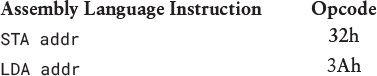
The abbreviation STA means “store accumulator,” and LDA means “load accumulator.” The abbreviation addr refers to a 16-byte address given in 2 bytes following the operation code.
The mnemonic HLT corresponds to the opcode 76h, which halts the CPU.
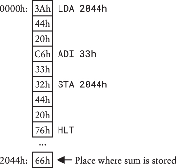
Here’s a little computer program that uses a few of these instructions, showing how the operation codes correspond to the assembly language instructions:

The LDA instruction loads the values at the address 2044h in the accumulator. That value is 66h. The MVI instruction loads the value 33h into register B. The ADD instruction adds the value in register B to the value in the accumulator. Now the accumulator contains the value 99h. The STA instruction then stores that sum to memory at the address 2044h, overwriting the value 66h with the value 99h.
The eight operation codes in the table on page 329 in Chapter 21 perform arithmetic and logical operations using the byte following the instruction code. Those instructions are shown here with their official Intel 8080 mnemonics:

I mentioned in Chapter 21 that these instructions are referred to as immediate instructions because they perform an arithmetic or logical operation using the byte immediately following the opcode. They can be pronounced “add immediate,” “add with carry immediate,” “subtract immediate,” and so forth. The operation always involves the accumulator, and the result goes back into the accumulator.
The little program shown previously can be simplified like so:
Now instead of loading the value 33h into register B and adding that to the accumulator, the value 33h is added to the accumulator with the ADI instruction.
The Intel 8080 also defines 63 instructions that move bytes from one register to another, from the memory address [HL] to a register, or from a register to that memory address:
These are called move instructions, abbreviated with the 8080 mnemonic MOV. These 63 instructions are written with both the destination register and source register. The code 69h is
MOV L,C
The destination register appears first, and the source register is second. Watch out! This convention can be confusing at first. This instruction means to move the byte in register C to register L. Perhaps you can visualize it like this, with a little arrow showing how the byte is moved:
The previous content of register L is replaced with the value from register C. The content of register C does not change, and afterwards C and L contain the same value.
Notice that seven of these instructions don’t really do anything because the source and destination registers are the same, for example:
MOV C,C
Moving the contents of a register to itself doesn’t do anything.
However, there is no MOV M,M instruction. That would be operation code 76h, which is instead used for the instruction that halts the computer, abbreviated HLT.
Here’s another way to write the little program that adds a value to the byte at memory location 2044h:
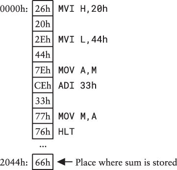
This version demonstrates the convenience of indirect addressing using the H and L registers. They are set just once to values that form a memory address of 2044h. The first MOV instruction moves the value at that address into the accumulator. The accumulator then contains the value 66h. Then the value 33h is added to that. The second MOV instruction moves the value of the accumulator to the memory location 2044h without needing to specify that address again.
If you examine the bits that make up these 63 MOV instructions, you’ll discover the following pattern:
where DDD is the destination register and SSS is the source register. This is the same table you saw earlier:
One way to design a CPU is to first decide what instructions you want the CPU to implement and then figure out what circuitry you need to do that. That’s essentially what I’m doing here. I’m selecting a subset of the Intel 8080 instructions and then building the circuitry.
To implement all the instruction codes that involve the seven registers, the CPU needs a way to store bytes in seven latches and to retrieve those bytes based on those 3-bit codes. For now, I will ignore the code 110 because it must be treated as a special case. The other seven codes can be used as inputs to 3-to-8 decoders.
The following circuit contains seven latches and seven tri-state buffers. One 3-to-8 decoder is used to latch the incoming value into one of the registers, and another 3-to-8 decoder is used to enable one of the tri-state buffers to select a value from one of the registers:
![]()

This is called a register array, and it is the most important circuit you’ll be seeing in this chapter. I know it looks a bit complex at first, but it’s really quite straightforward.
At the top of the circuit is an 8-bit data path labeled “In.” That’s a byte to be saved in the register array. The seven boxes labeled with letters are 8-bit latches. Although not explicitly labeled, each of these latches has a Clock input on the left that saves a value in the latch.
At the top of the diagram on the left and right are two 3-to-8 decoders with Select inputs labeled S2, S1, and S0. The values of these Select inputs correspond with the codes for the seven latches as shown in the previous table. That’s why the output labeled 6 is unused: That output corresponds to a select value of 110, which refers to a memory location rather than a latch.
The 3-to-8 decoder on the top left controls the Clock inputs on these latches. That Clock signal is routed to one of the seven latches depending on the values of S0, S1, and S2. This process saves the input byte in one of the latches.
Underneath each of the seven latches is a tri-state buffer. Although not explicitly identified, each of these buffers has an Enable input. On the upper right is another 3-to-8 decoder. This decoder enables one of the seven tri-state buffers, and the byte stored in that latch appears at the Out data path at the bottom.
Notice that the accumulator is treated somewhat specially here: The value stored in the accumulator is always available as the Acc output shown at the bottom.
The 8-bit values going into this register array can come from several sources: They can come from memory, or from one of the other registers, or from the ALU. The 8-bit values coming out of this register array can be stored in memory, stored in one of the other registers, or go into the ALU.
Just so you don’t lose sight of the forest while wandering around the trees, here’s a simplified block diagram that shows these data paths:

Much is missing from this diagram. Only shown are the major 8-bit data paths. Besides the path from the Acc output of the register array to the A input of the arithmetic logic unit, all the other inputs and outputs are interconnected. Even the Data Output of the RAM is connected to the RAM Data Input!
This is possible because all the outputs of these components go through tri-state buffers, only one of which is enabled at any time. That enabled value can then be stored in memory with the Write signal, or stored in one of the seven registers in the register array, or a result of an arithmetic or logical operation can be stored in the ALU.
The connection between all the inputs and outputs is called a data bus. It’s a data path that is common to the inputs and outputs of all the components. When a tri-state buffer connected to the data bus is enabled, that byte is available all over the data bus, and it can be used by any other component on the data bus.
This data bus is only for 8-bit data. There will be another bus for the 16-bit memory address because that address can also come from a variety of sources. That 16-bit bus is called the address bus, and you’ll see it shortly.
Now for some annoying details. I sincerely wish that the register array were as simple as the circuit that I showed you on page 344, but it’s going to need a couple of enhancements.
The register array that I’ve shown you is great for the MOV instructions that involve moving a byte from one register to another. Indeed, the 3-to-8 decoders were implemented in the register array with the MOV instruction in mind: The contents of one register can be enabled on the data bus, and that value can be stored in another register.
But this register array doesn’t work for the STA and LDA instructions. Those instructions store a value from the accumulator into memory and load a value from memory into the accumulator. Other instructions also involve the accumulator. All the arithmetic and logic instructions store the result in the accumulator.
For that reason, the accumulator section of the register array must be enhanced somewhat to allow a value to be stored in the accumulator and later retrieved from the accumulator independently of the 3-to-8 decoders. This can be accomplished with just a little additional logic in the register array that involves only the accumulator latch and tri-state buffer:
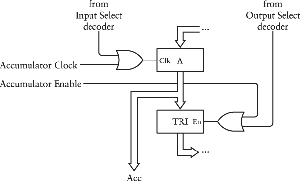
Two additional signals at the left have been added that are inputs to two OR gates. These signals allow a value from the data bus to be saved in the accumulator (the latch labeled “A”) independently of the Input Select decoder and to be enabled on the data bus independently of the Output Select decoder.
Another enhancement to the register array is required for addressing RAM with the combination of the H and L registers. But that enhancement is much more severe, so let’s delay it as long as possible while focusing on other necessities!
Three additional 8-bit latches must be connected to the data bus. These are the latches that store the instruction bytes:
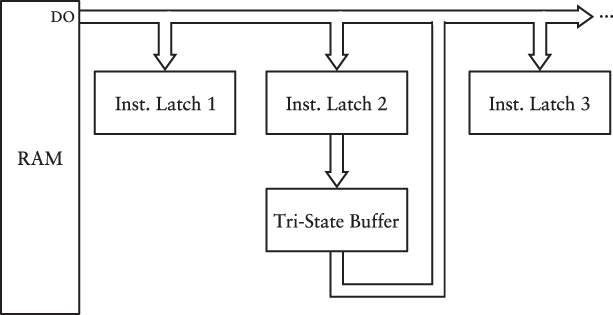
The operation code is always stored in Instruction Latch 1. After the operation code is stored in the latch, it can be used to generate all the other signals that control the CPU. You’ll see how this works in the next chapter.
Instruction Latch 2 is used for instructions that have an additional byte. For example, the move immediate (MVI) operation codes are followed by a byte that is then moved into one of the registers. The arithmetic and logical immediate instructions, such as ADI, are also followed by a byte. In the case of ADI, for example, that byte is added to the accumulator. The value in Instruction Latch 2 must therefore be enabled on the data bus, which is the purpose of the tri-state buffer.
Instruction Latches 2 and 3 are used together for those instructions that are 3 bytes in length—for example, STA and LDA. For these instructions, the second and third bytes constitute a 16-bit value used to address memory.
Aside from the 8-bit data bus, the CPU requires a 16-bit address bus to access up to 64K of memory. From what you know so far, the address used to access memory can come from three different sources:
A value called the program counter. This is the 16-bit value that accesses instructions. It starts at 0000h and sequentially increases until a
HLTinstruction.The 2 bytes following the
STAorLDAoperation codes. Together these form a 16-bit address.The H and L registers form a 16-bit address—for example, in the
MOV A,Minstruction. When used in this way, HL is called a register pair.
In the Triple-Byte Accumulator, memory was accessed sequentially using a 16-bit counter. I’m not going to use a counter with the CPU that I’m building. As you’ll see in Chapter 24, some instructions can set the program counter to a different address. For that reason, the program counter will be a 16-bit latch whose value is generally increased by one after an instruction byte is retrieved from memory.
Here’s the program counter in its entirety:
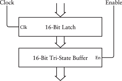
Notice that these data paths are visibly wider than those shown in earlier diagrams because they represent 16-bit values. Both the input at the top and the output at the bottom are connected on the address bus. Any value on the address bus can be saved in the latch using the Clock input, and the value in the latch can be put on the address bus using the Enable signal.
For an STA or LDA instruction, the 2 bytes following the operation code are stored in Instruction Latches 2 and 3. This means that those latches must also be connected to the address bus through a tri-state buffer.
For a MOV instruction that involves a memory address with the HL register pair, the values from the H and L latches must also be connected to the address bus. When building the register array, I gave no thought at all to this requirement. In my design of the register array, the H and L registers only come in contact with the data bus.
Moreover, I want to introduce two more instructions:

The INX instruction adds 1 to the 16-bit value in the register pair HL. The DCX instruction performs a decrement by subtracting 1 from the value.
These instructions turn out to be very useful, particularly INX. For example, suppose there are 5 bytes stored sequentially in memory starting at address 1000h, and you want to add them up. You only need to set the H and L registers once and then increment the value after accessing each byte:
You’ll recall that the ALU has some flags that indicate when the result is zero, or if it’s negative or if a carry has resulted from an addition or subtraction. No flags are affected by the INX and DCX instructions.
(The Intel 8080 also implements INX and DCX instructions for the register pairs BC and DE, but those are less useful, and I won’t be implementing them in my CPU. The Intel 8080 also implements 8-bit increment and decrement operations, abbreviated INR and DCR, for all seven registers and memory addressed by HL, but I won’t be implementing those instructions either.)
The INX and DCX instructions imply that we need some additional circuitry to perform a 16-bit increment and decrement.
I mentioned earlier that the program counter—the latch used to store the 16-bit value that accesses instructions from memory—must also be incremented after each byte of an instruction is read from memory. A 16-bit increment is needed here as well.
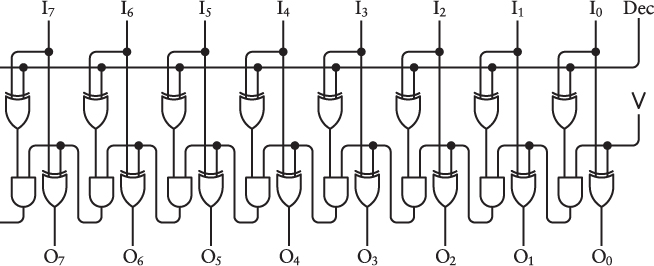
An increment and decrement circuit is somewhat simpler than an adder and subtracter because it only has to add and subtract the number 1. Here’s an 8-bit version just so you get an idea of what it looks like. The subscripted I’s are inputs; the subscripted O’s are outputs. The Dec input signal is set to 0 for incrementing the value, and 1 for decrementing the value:
Let’s put this assemblage of XOR and AND gates in a larger component that includes a 16-bit latch to store a value that needs to be increased or decreased by 1, and a tri-state buffer that provides the incremented or decremented value:
![]()

Let’s call this component the incrementer-decrementer. As with the program counter, the 16-bit input to the latch and the 16-bit output from the tri-state buffer are both connected to the address bus. Either the Decrement or Increment input signal can enable the tri-state buffer, but the Decrement signal decrements the value in the latch, while the Increment signal increments it.
The 16-bit address bus is primarily for providing an address to the RAM, but it must also be capable of moving 16-bit values among components of the CPU.
For example, the program counter is used to address RAM when accessing instructions from memory. After the value in the program counter accesses an instruction, the value must be moved into the incrementer-decrementer to be incremented and then saved back in the program counter latch.
Another example: A MOV A,M instruction uses the HL register pair to access a byte from memory. But often this is followed by an INX HL instruction that moves the value of HL into the incrementer-decrementer to be increased by 1 and then saved back into the HL register pair.
Finally, the problem I’ve been avoiding can be avoided no longer. The register array I showed you earlier is very neat and elegant and lovely, but it doesn’t provide a way to put the values of the H and L on the 16-bit address bus. Here’s a fix for that:
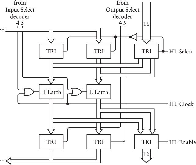
Notice the 16-bit inputs and outputs on the far right. Both of those will be connected to the address bus to allow saving a 16-bit value in the H and L registers and to retrieve it.
That diagram enhancing the H and L registers shows several new signals and components that have been added to the register array:
The HL Select signal at the right controls the top row of new tri-state buffers. The signal determines whether the inputs to the H and L registers come from the normal input to the register array or from the 16-bit input.
The HL Clock signal at the right goes into two OR gates that have been added to the Clock inputs of the latches to allow saving values from the address bus.
The HL Enable signal at the right enables a new 16-bit tri-state buffer so the composite output of the H and L latches can appear on the address bus.
What a mess! But nobody ever claimed that building a computer was easy.
![]()
An interactive version of the complete register array is available on the website CodeHiddenLanguage.com.
Now let’s connect these 16-bit components to a 16-bit address bus. The following block diagram shows part of the data bus at the top as input to Instruction Latches 2 and 3, the outputs of which are combined in a tri-state buffer connected to the address bus:

The visibly wider 16-bit address bus itself circles around the components at the bottom as both inputs and outputs, and it also supplies the address to the RAM.
Like the earlier block diagram of the data bus, this block diagram of the address bus is missing a few essential signals: signals to enable the tri-state buffers, and signals to save the value on this bus in various latches.
It is these signals—properly coordinated and synchronized—that cause instructions to be executed by the CPU. It is these signals that are the pulsing life force of the computer, and they deserve their own chapter. That’s up next.