Making and editing footprints
Abstract
Footprints provide a means of physically attached components to your printed circuit board (PCB), and they provide electrical connectivity as defined by the netlist generated in Capture. Footprints in PCB Editor are known by several names, including symbols, components, and packages. The PCB Editor library has over 400 symbols, but there will be occasions when you will need to make your own. This purpose of this chapter is to
- 1. introduce PCB Editor’s symbol libraries,
- 2. discuss the composition of a footprint,
- 3. provide a detailed explanation of padstacks,
- 4. demonstrate how to create a padstack using the Padstack Editor,
- 5. provide footprint design examples, and
- 6. provide design examples for mechanical symbols and flash symbols.
Keywords
Printed circuit board; plated through holes; pin-grid array; ball grid array; design rule checker; Package Geometry; padstack; footprint
Footprints provide a means of physically attached components to your printed circuit board (PCB), and they provide electrical connectivity as defined by the netlist generated in Capture. Footprints in PCB Editor are known by several names, including symbols, components, and packages. The PCB Editor library has over 400 symbols, but there will be occasions when you will need to make your own. This purpose of this chapter is to
- 1. introduce PCB Editor’s symbol libraries,
- 2. discuss the composition of a footprint,
- 3. provide a detailed explanation of padstacks,
- 4. demonstrate how to create a padstack using the Padstack Editor,
- 5. provide footprint design examples, and
- 6. provide design examples for mechanical symbols and flash symbols.
Introduction to PCB Editor’s symbols library
The standard PCB Editor footprint library is located in the special folder of the OrCAD® installation path, for example, “C:CadenceSPB_17.2sharepcbpcb_lib”. In that folder, there are two more folders: devices and symbols. The devices folder contains text files that define logic information for certain component types, which are not discussed here. The symbols folder contains eight types of files. Table 8.1 lists the files and explanations of their functions.
Table 8.1
Some files have the same file name but different file extensions, for example, the cap300.dra file and cap300.psm file. In general, you work with the .dra files with PCB Editor, then PCB Editor creates the other files that it actually uses in a board design.
For each type of file, PCB Editor operates in a particular mode. When you open an existing drawing (.dra) file, PCB knows which mode to be in as it reads the file and knows the corresponding symbol file (.bsm, .psm, etc.). When you start a new drawing (.dra) file, you select the mode by choosing a drawing type from a list. When you finish working with the .dra file and save it, PCB Editor automatically creates the correct symbol file. This is demonstrated in the examples that follow.
Symbol types
Package symbols (name.dra and name.psm) are the component footprints used on your board design that are assigned in Capture. After finishing the footprint drawing the .psm file is generated when you save the drawing.
Mechanical symbols (name.dra and name.bsm) are objects, such as mechanical pins, which are not connected to a net, mounting holes on boards, or predefined board outlines. The mechanical pins don’t have the pin number, and there is no need to include such pins to the Schematic.
Flash symbols (name.dra and name.fsm) are used to define thermal reliefs, which are used to connect padstacks to power and ground planes when the planes are defined as negative plane layers. Positive plane layers do not need flash symbols, because PCB Editor automatically creates thermal reliefs based on trace width and spacing settings as defined in the Constraint Manager (more on that in PCB Design Examples in Chapter 9). Also flash symbols can be used to create the array of openings in the pastemask stencil.
Drawing formats (name.dra and name.osm) are predefined drawing templates that follow standard paper sizes. The six drawing formats range from drawing size A (8.5×11 in.) to size E (44×34 in.). You can add these to your board designs to give them a professional look and follow industry drawing standards.
Custom pad shapes (name.dra and name.ssm) are specially designed shapes used to create padstacks that have pad shapes other than round or rectangular/square pads.
Padstack files (name.pad) define surface-mount and through-hole padstacks and include conductor information, such as inner and outer pad shape and size, and thermal relief sizes and physical information, such as drill diameter and soldermask and pastemask shapes and sizes. Padstack definitions are handled using an application called Padstack Editor, which can be launched from within PCB Editor (Tools menu) or launched separately from the Windows Start menu. Padstack Editor is demonstrated in the design examples that follow.
Composition of a footprint
A footprint symbol is made up of pins (padstacks), graphics (for outlines etc.), and text. As an example, Fig. 8.1 shows the through-hole resistor symbol res400.dra found in the symbols library. To view it, open PCB Editor, navigate to the symbols folder, and select the .dra file type and then select the res400.dra. Table 8.2 describes what the objects are and to what class and subclass each object belongs. As described earlier the pin (padstack) is actually defined by the Padstack Editor and simply inserted into the symbol drawing along with the graphics and text objects.

Table 8.2

Padstacks
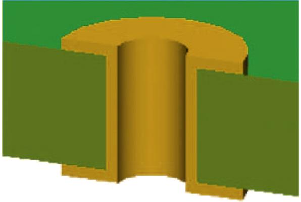
Fig. 8.2 shows an example of a multilayer padstack from a PCB’s perspective. Padstacks define every aspect of how a component’s pins will be fastened to the PCB and how traces will be connected to them. Padstack definitions specify areas for copper pads on outer and inner routing layers, thermal reliefs and clearance areas in plane layers, openings in soldermasks, and solder paste (optional). From the PCB designer’s perspective the drill hole may also be considered part of the padstack definition, but the copper used to plate through holes and vias is not. This is because the plating thickness is controlled by the board manufacturer and is typically insignificant relative to the drill and lead diameters. More about the lead-to-hole diameter is discussed in a later example and Chapter 5, Introduction to design for manufacturing.
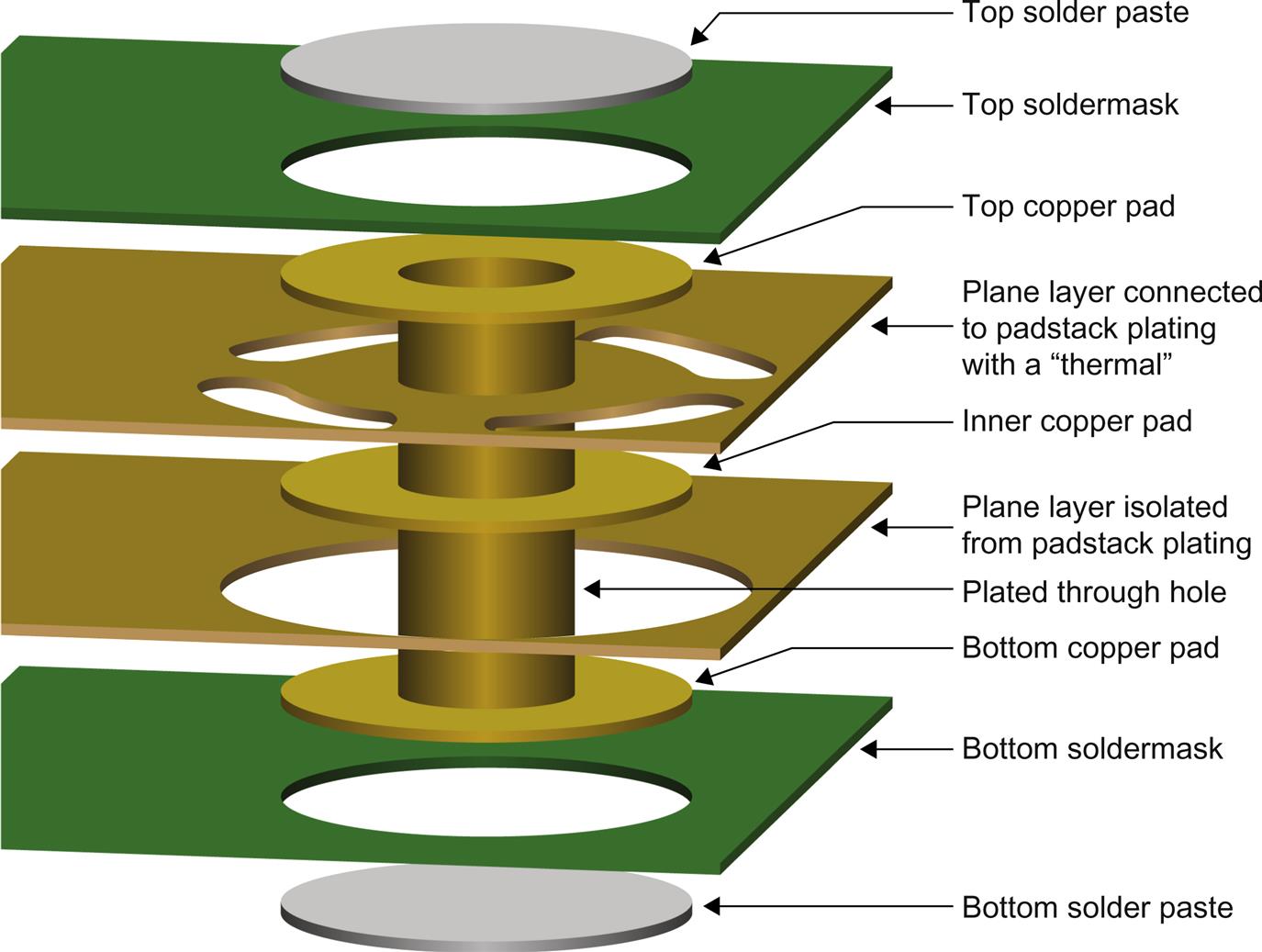
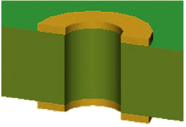
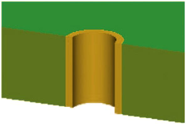
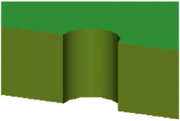
Fig. 8.3 shows how a padstack is actually displayed in PCB Editor. When a particular layer is made active (using the Options pane), the pad on that layer is brought to the front of the view, while pads on inactive layers are pushed behind. Padstacks have clearance areas defined, which remove copper from plane layers and are visible when the plane layers are visible. The pin number of the padstack is displayed if the Pin_Number subclass box is checked in the Package Geometry class in the Color Dialog panel. Drill holes are also displayed if the Display / Plated Holes option is enabled in the Design Parameter Editor as shown in Fig. 8.4.


Graphical objects
Graphical objects (lines, arcs, etc.) are placed on footprints and board layouts to show information not defined by padstacks (such as the outline of a part). The objects may be visible on the final board or visible only in the design files. Objects that are visible on the board include silk-screen markings (component outlines, for example), while objects visible only in the design files include things such as board outlines, assembly outlines, and boundaries (e.g., keep-out areas where traces and components are not allowed).
Several types of objects can be used in PCB Editor, but usually only three or four types are used when making footprints (i.e., detail objects, place boundary outlines, and occasionally copper areas). Detail objects are used to indicate silk-screen markings that will be visible on the board and on assembly layers to provide information during assembly. Place boundary outlines are used by the design rule checker (DRC) utility to maintain required distance between parts while laying out the board. On routing layers, copper areas can be used as heat spreaders or mini-ground planes for components that require them. Examples of how to use these objects are given in the PCB Design Examples (Chapter 9).
Text
Like graphics, text objects can be visible on a PCB or visible only within the design files. Text objects on PCBs are often part of the silk screen and may be used for such purposes as component reference designators (part of the footprint silk screen) and displaying board serial numbers or design revisions (part of the board silk screen). Text that is visible only in the design files might be placed on one of the assembly or documentation layers to show board dimensions or special manufacturing instructions.
Minimum footprint requirements
As shown in Fig. 8.1, many types of text and graphics objects can be used when you make a new footprint. Not all the items shown in the figure are required, but four minimum objects are required on a footprint design. Packages must have the following elements: (1) at least one pin, (2) at least one reference designator, (3) a component outline, and (4) a place-bound rectangle. As shown in Table 8.2, reference designators and component outlines are placed on the silk-screen or assembly layers (usually both), and the place-bound rectangle is on the Place_Bound_Top (or Bottom) layer.
Optional footprint objects
The following is a list of other elements you can add to a package symbol during the symbol building process:
- • Device type (text for the component device type).
- • Component value (text for the component value).
- • Tolerance (text for the component tolerance).
- • Component height (text for the physical height of the component).
- • User part number (text for the package part number).
- • Route keep-out shapes, identifying areas where etch is not allowed.
- • Via keep-out shapes, identifying via keep-out areas.
- • Etch (etch lines, arcs, rectangles, shapes, or text added to the symbol).
- • Vias.
For further reading on design requirements, please see Chapter 4, Introduction to industry standards, for a list of industry standards and Appendix B for more information on packages and footprints.
Good sources for package information can be found at the following websites:
- • IPC website (www.ipc.org)
- • www.PCBLibraries.com/downloads—Land Pattern Calculator based on the IPC-7351B standard
- • http://www.onsemi.com/PowerSolutions/supportDoc.do?type=drawing
- • http://www.ti.com/support-packaging/packaging-information.html
- • www.diodes.com/datasheets/ap02002.pdf
Introduction to the Padstack Editor
The two basic kinds of padstacks are through-hole padstacks (for leaded components and vias) and surface-mount pads. Through holes are made using padstacks that allow connections from any one layer to any other layer (as in Fig. 8.2). Surface-mount pads are isolated from all layers except for the top layer and therefore do not use drilled and plated holes. Surface-mount pads may be on the top or bottom layer (or both in the case of edge connector footprints). Connecting a surface-mount pad to another layer is accomplished using a special padstack called a fan-out via (also called a stringer pad). A fan-out via is usually not part of the footprint; it is added to a PCB when placing parts and routing traces. You will see how to do this in the PCB Design Examples (Chapter 9).
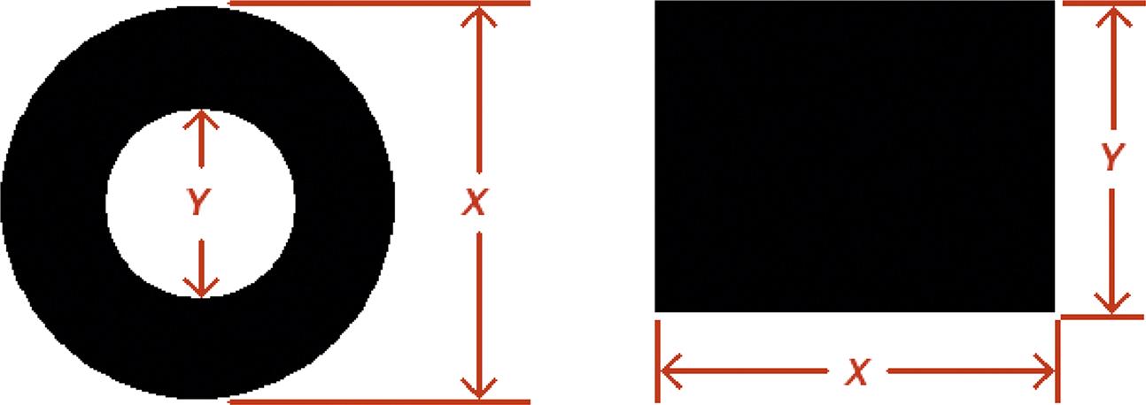
Through-hole padstacks are often named by their shape and size. The typical pad geometries are null, circle, square, oblong, rectangle, rounded rectangle, chamfered rectangle, octagon, donut, n-sided polygon, and user-defined shape. For circular through-hole padstacks, one naming convention used is padXcirYd.pad, where pad indicates padstack, X is the pad outer diameter (OD), cir is the circular shape (sq for a square top pad or rec for rectangular), and Y is the pad inner diameter (ID)—the drill size (see Fig. 8.5). For example, if the outer dimension of a round pad is 62 mil (0.062 in.) and the drill hole is 25 mil, the pad name would be pad62cir25d.pad.
For surface-mount pads a typical naming convention is smdXrecY.pad (or smdX_Y.pad), where smd indicates the padstack, which is for a surface-mount device, X is the pad width, rec (or _ ) indicates a rectangular pad, and Y is the pad height.
Through-hole and surface-mount pads are designed and modified using the Padstack Editor (see Fig. 8.6). There are two ways to launch the Padstack Editor.
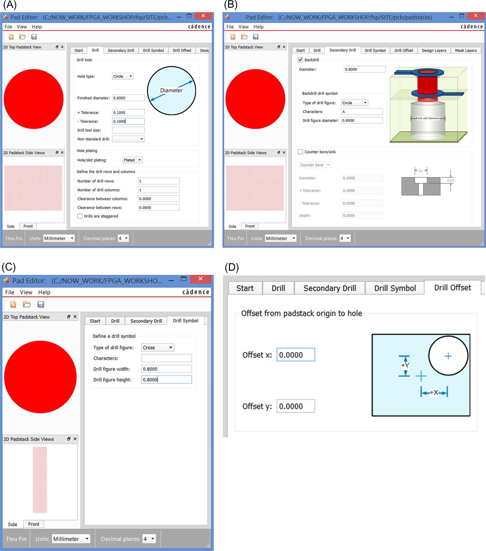
Padstack Editor can be launched from within PCB Editor or separately from the Windows Start menu. In the PCB Design Examples (Chapter 9), it will usually be launched from within PCB Editor. In the footprint design examples that follow, Padstack Editor will be launched from the Windows Start menu, where detailed instructions on how to use it are provided in the examples. Padstack Editor has several tabs, arranged from left to right in the sequence of steps required to create the new padstack.
Start tab
Here you can define the Type (usage) and Shape (geometry) of new pad.
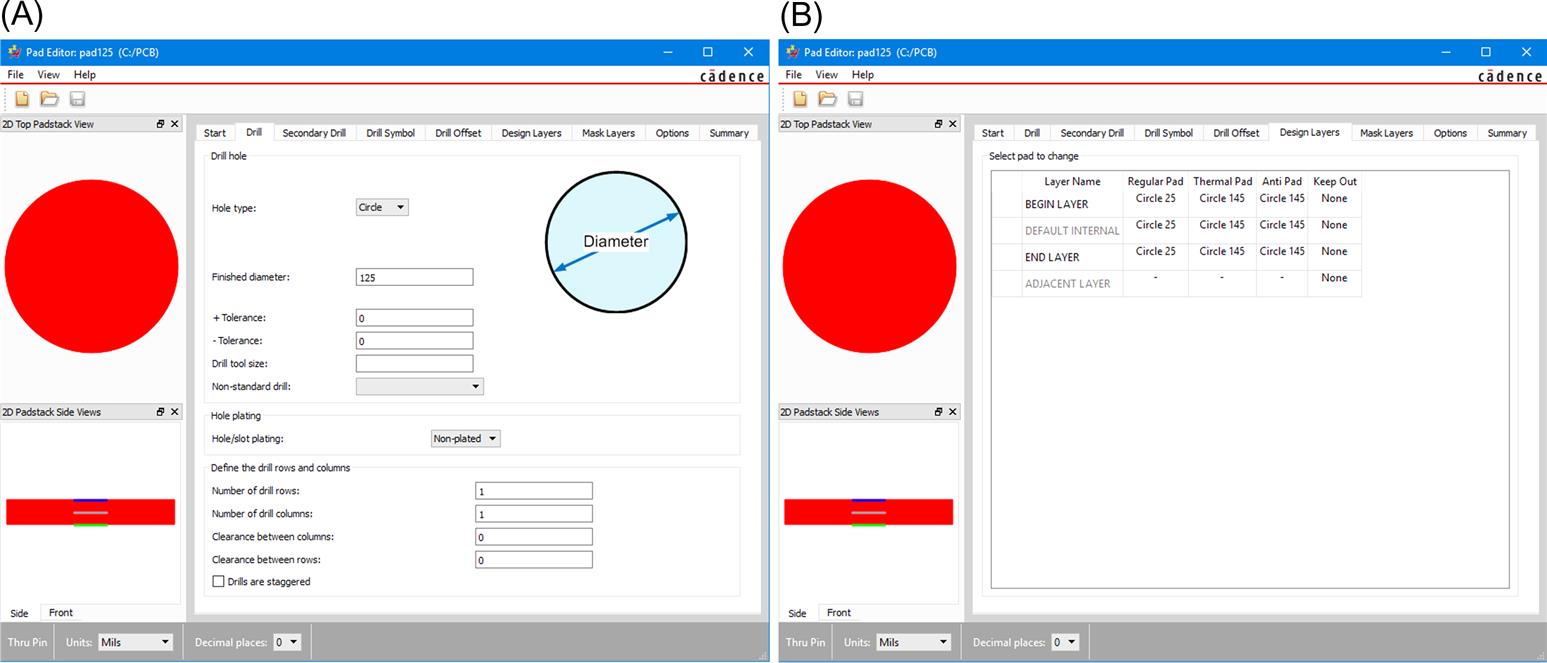
Drill tab
The Drill tab (Fig. 8.6A) is where the drill diameter and related parameters are set.
Hole type—the shape of the hole, typically Circle, but you can also choose Square for some special technology reasons.
Finished diameter—the diameter of the hole after plating. Usually this is more important value than the drill tool diameter, because for the assembly reasons we need to know the finished diameter.
± Tolerance—the tolerance of the hole size, typically ±0.1 mm, but for the press-fit holes it can be set as ±0.05 mm.
Drill tool size—the optional field to set up the tool size. If not specified, the PCB manufacturer will choose the tool diameter according to the technology used, based on needed finished diameter value. Some component assembly techniques require a specific hole size for correct assembly.
Nonstandard drill—you can optionally choose a specific technology to make the hole, such as laser, plasma, and punch.
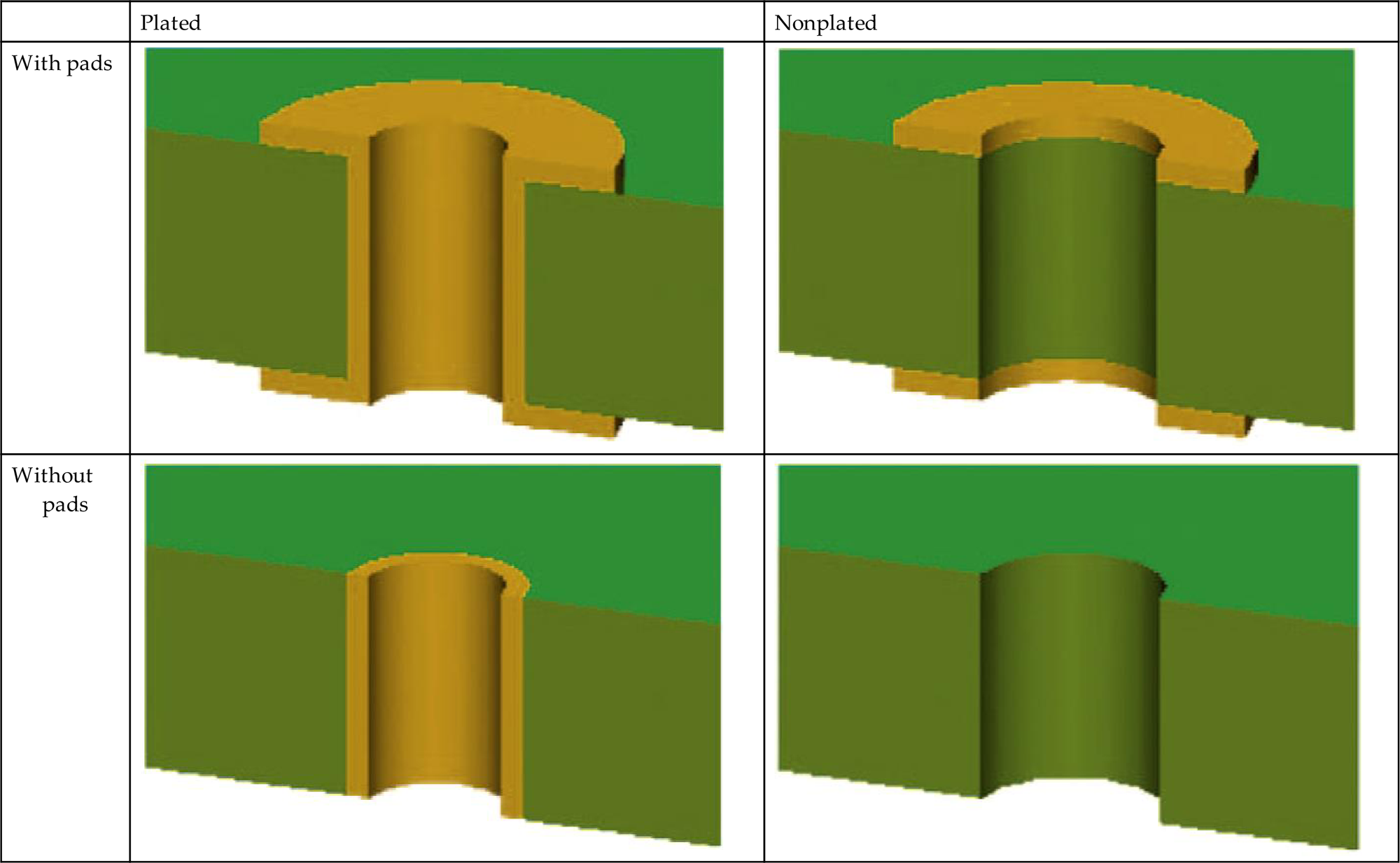
Hole plating—here you should choose if the hole is plated, or nonplated. Note that Padstacks of Thru Hole Type are always plated according to the IPC-2581B standard.
Define the drill rows and columns—if you need the array of the holes located inside the pad.
Units—this field in the left-bottom corner of the window allows you to choose the measurement units. It’s recommended to use millimeter or mils.
When you enter the hole parameters, you can see it on the left, in 2D Top Padstack View and 2D Padstack Side View windows (the Side View window, in its turn, allows to see the Side and Front cross section of the hole).
Secondary Drill tab
This allows you to define the secondary drill parameters. This operation is needed if you want to make additional drilling over the hole, for example, the backdrilling for high-speed signals (remove the extra part of the plated hole in thick PCB, to reduce the reflections and to improve the Signal Integrity), or the counterbore for the mounting holes.
Diameter—the tool diameter of backdrilling, which is usually 0.3…0.4 mm bigger than the finished plated hole diameter.
Type of drill figure—the graphics symbol of this hole on the drawing.
Characters—additional text inside of the drill figure.
Drill figure diameter—the size of the drill figure.
Drill Symbol tab
In this tab, you can define the drill figure for the drawings. This definition is not fixed and can be overridden later in the PCB.
Type of drill figure—the shape of the figure.
Characters—the additional text inside the figure.
Drill figure width/height—the size of the figure—typically equal to the hole size.
Drill Offset tab
If you need to shift the hole from the center of pad, you can use the Drill Offset tab.
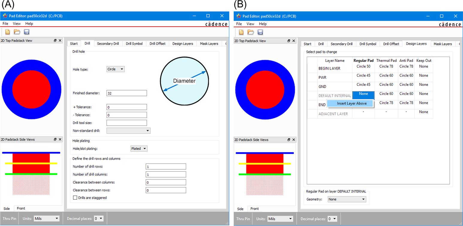
Design Layers tab
In Fig. 8.7A the layer stack-up definition consists of a beginning layer (TOP), a default internal layer, an ending layer (BOTTOM) and the associated soldermasks. In Fig. 8.7B the layer stack-up definition consists of just a beginning layer (TOP).
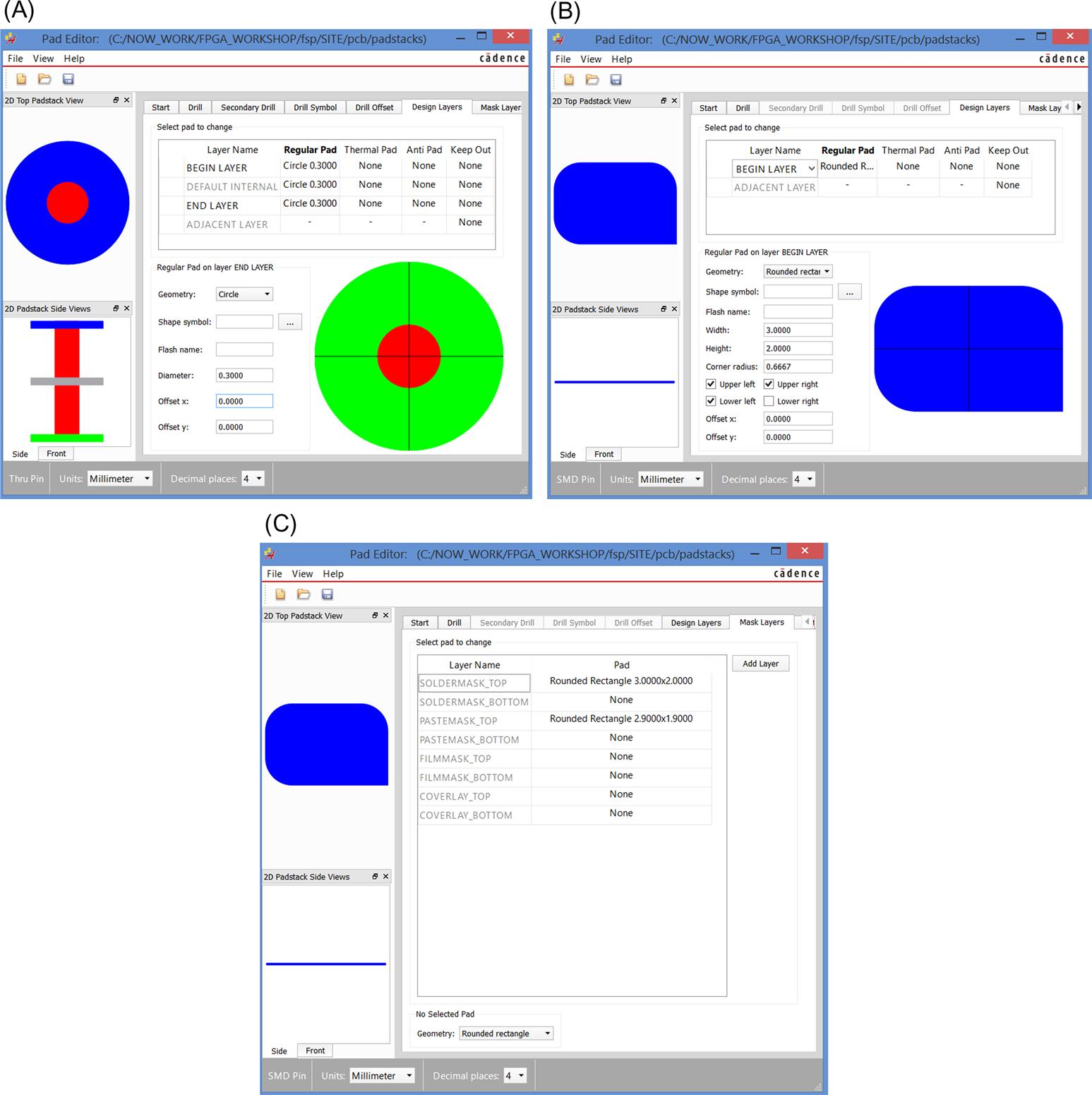
Begin Layer/Default Internal/End Layer—here you should choose the pad shape and size for the beginning, inner, and end layers. Default Internal—any internal layer of the multilayer PCB. Note that it’s no need to create in advance all types of blind or buried vias from scratch. Instead, in OrCAD PCB Editor, you can just select some existing plated through hole (PTH) or blind via as a template and simply create from it the new blind/buried via, with new name and new set of start/end layers.
 Browse… button
Regular Pad—choose any of standard shapes. If your pad should have nonstandard shape, you can choose the Shape Symbol, where the polygon of needed special shape can be drawn. To see the list of available shape symbols, press the Browse “…” button,  , on the right of shape symbol name. Then, if you don’t see the appropriate shape symbol in the list, push the “Create new Shape Symbol” button, set its name, and the PCB Editor window will open. Then you should draw the single polygon of needed size and shape located in the 0,0 point in the ETCH/TOP layer (which should be used for any shape symbol). Then save the shape symbol file to the proper path (e.g. /share/pcb/pcb_lib/symbols) and close the PCB Editor. Now you will see the created Shape Symbol in the list, you can choose it to place to the needed layer of your padstack.
You can see the shape and size of the pad in the right bottom corner of the Padstack Editor window (see Fig. 8.7).
Thermal Pad/Anti Pad/Keep Out—these fields allow to set up the spacing of the pad in the negative plane layers for thermal connection and for nonconnected pads, as well as the route keep-out area for mechanical hole or under the surface-mounted device (SMD) pad in adjacent layer, for example, if you need to decrease the SMD pad capacitance and improve the signal integrity. Actually, you can leave these fields blank, because it’s better to set the spacing parameters later, globally for all pads and vias in the PCB project.
Mask Layers tab
Here you can set the openings in the soldermask and pastemask layers, as well as the coverlays for rigid-flex PCBs and any other types of masks. You can create your own types of mask layers. The standard types of masks are listed below.
Soldermask TOP/BOTTOM—you should make the opening in the soldermask a little bit larger than the pad size, usually by 2 mil (0.05 mm) each direction. Ask your PCB supplier for the correct value.
Pastemask TOP/BOTTOM—the size of the opening in solder paste stencil depends on the assembly house. Normally it is a little bit smaller that the pad size, about 1 mil (0.025 mm) each side. For the large pads, it’s recommended to split the pastemask opening to several smaller openings, which will cover not more than 50% of the pad area. For this purpose you can create the Flash Symbol file (similarly to Shape Symbol described earlier) and use it.
Filmmask_TOP/BOTTOM—the user mask which you can use for such tasks as capped via masks or plugged/tented vias.
Coverlay_TOP/BOTTOM—this mask is used to create the openings in the flexible part of PCB, in polyimide coverlay material. Usually the size of the opening is smaller than the pad size by 2 mil (0.05 mm) each side.
Options tab
In the Options tab, you can manage two parameters.
Suppress unconnected internal pads—to improve the manufacturability and signal integrity by removing the pads in the inner layers, if they are not connected to the traces or shapes. Contact to your PCB supplier to understand if this option will be acceptable.
Lock layers span—use this option while creating the blind via if you don’t want to allow to insert the new layer between the start and end layers of this blind via.
When you have filled all needed values and parameters, you can check everything in the Summary tab and then save the padstack file to the proper folder. It is recommended to create the special folder for the user created pads, shape symbols, and footprints. Then in PCB Editor User Preferences, you should add this folder path to the padpath and psmpath preferences, to let PCB Editor know where the user padstacks and footprints are located.
Footprint design examples
Three footprint design examples are given. Before starting any footprint design, it is best to have the correct padstacks predefined, as it makes the design process go more smoothly. In each example, Padstack Editor is used to locate existing padstacks or design new ones.
The first design example demonstrates how to design a through-hole footprint from scratch. The second design example demonstrates how to modify an existing, surface-mount footprint to create a new one. The last example demonstrates how to use the Symbol Wizard to design a high pin-count pin-grid array (PGA) footprint.
Example 1. Design of a through-hole device from scratch
In this design example the footprint for a 1/4-W, 20%, carbon film resistor will be made. For this resistor the lead diameter is 25 mil, the body length is 250 mil, and the body width is 100 mil. An example is shown in Fig. 8.8. The component is similar to the res400 symbol that exists in the symbols library, but we design our own to learn the process, then we can compare the two.

Designing the through-hole padstack
Using the procedures described in Chapter 5, Introduction to design for manufacturing, the calculated hole diameter should be between 33 and 56 mil, and the pad should be between 51 and 74 mil for a Class A board design (using the IPC method). Several padstacks in the symbols library meet this requirement, but one that does not exist will be chosen so that the design process can be demonstrated. So, if we decide that, in addition to these requirements, we want an annular ring width of 10 mil, then a padstack with a drill hole diameter of 42 mil and a pad diameter of 62 mil suffices. The typical naming convention in PCB Editor for a pad with these dimensions is pad62cir42d, which does not exist in the native symbols library. To create this padstack, launch Padstack Editor by selecting Start → All Programs → Cadence Release 17.2-2016 → Padstack Editor, or just find the Padstack Editor in the list of applications (depending on operating system version that you use). A blank, unnamed padstack will be opened.
In the Start tab, choose the type of new padstack—Thru Pin and select the pad geometry—Circle. Switch to the Drill tab and enter the remaining values as shown in Fig. 8.9. You can choose any of the available drill symbol figures in the Drill Symbol tab. The size of the drill figure is not critical but is typically about the size of the drill diameter or a little smaller. Note that the drill symbol will not be visible initially when you ultimately place the component on the board. The drill symbol becomes visible only after you place a drill table in the design.

Next select the Design Layers tab. Enter the values shown in Fig. 8.10A. To enter values for a particular layer, select the layer by left clicking the row in one of the three columns to the right. If you left click the row in the name column, the name will be highlighted so that you can change its name.
- • Regular Pad. The values on the internal layers can be identical to the outer layers but often they are slightly smaller (anywhere from 0 to 20 mil difference in diameter depending on the size).
- • Thermal Pad. The native padstacks in the symbols library typically use circles that are the same size as the Anti Pad. But if you use negative artwork layers in your design, you need to use Flash symbols for the thermal pads. Flash symbols are described later, so for the time being leave the thermal pad as a circle. The procedure for defining padstacks that have no thermal pads (i.e., completely connected to a plane) is described later.
- • Anti Pad. The clearance between a pad (or hole) and the surrounding copper (e.g., on a plane layer) should be similar to or larger than the trace spacing constraints you will likely use in your design. A typical clearance diameter is 10–20 mil larger than the pad diameter. Note that, if you make an inner pad much smaller than the outer layer pads, the Anti Pad on the inner layer should still be larger than the largest pad in the padstack; otherwise undesirable capacitive coupling can occur between the larger pad and an adjacent plane layer (see the discussion in Chapter 5: Introduction to design for manufacturing). This parameter is important only if you use negative artwork layers in your design.
- • Keep Out. There is no need to set the route keep-out area for through-hole padstack, so we can leave it blank.

Before moving on to the next step, it would be a good idea to save your work to this point. When saving padstacks that you plan to use in active designs, you need to save them to the PCB Editor symbols folder or your working folder. Otherwise, if the design is just for practice, you can save it anywhere you like. When you save it for the first time, select Save As… from the File menu. After that you can just select Save from the File menu to save changes.
Select the Mask Layers tab. Set the Circle openings size in SOLDERMASK_TOP and SOLDERMASK_BOTTOM layers. Soldermask openings are usually a little larger than the outer pads so that registration tolerance errors will not cover any of the pad. The exact amount really depends on the capabilities of your board manufacturer, but in general the soldermask opening is typically 4–8 mil (0.1–0.2 mm) larger than the outer pad.
When you complete the entries shown in Figs. 8.9 and 8.10 save your design.
Designing a through-hole footprint symbol
When a new symbol drawing is first opened, the drawing area is quite large by default. So before opening a new drawing, it is a good idea to have an idea of what the footprint dimensions will be, so that it is known how large the drawing area should be. From the preceding description the body length is 250 mil, and the width is 100 mil. The footprint needs to be larger than that to account for the lead extensions, padstack dimensions and placement, and any other details that you might want to add to the drawing.
Using the procedure described in Chapter 5, Introduction to design for manufacturing, the padstacks are placed 400 mil apart. The diameter of each pad is 62 mil, so the drawing area should be another 200 mil or so wider. Silk-screen and assembly details and text are also added, so at the very least the drawing area should be 1000 mil square. The next thing to consider is where the origin of the part will be. Through-hole components often have their origins on pin 1. Surface-mount components typically have their origins at the body center. Since this will be a through-hole component, we put the origin on pin 1. Starting at the lower left corner the (x, y) coordinate will be (−1000, −1000), and we make the working area 3 in. wide by 2 in. tall.
To begin making a new footprint, open Start → All Programs → Cadence Release 17.2-2016 → PCB Editor. PCB Editor will open the last design you worked on by default. Start a new footprint drawing by selecting File → New… from the menu bar. The New Drawing dialog box will be displayed (see Fig. 8.11). Enter a name in the Drawing Name: box for the new footprint and click the Browse… button to choose a location for the new footprint. If you have a project folder setup for your design, you can save it there. Otherwise save it in the symbols library. Select Package symbol from the Drawing Type: list (we will use the package Symbol Wizard in a later example) and click OK. Note that, at the beginning of the chapter, it was told that PCB Editor will be in a specific mode depending on what type of drawing you are making; this is where the mode is set.

When the new design is opened, a PCB Editor window will be displayed that looks just like a board design window.
The first thing that needs to be done is to set up a drawing area that is practical for this design. Select Setup → Design Parameters… from the menu bar. At the Design Parameter Editor dialog box, select the Design tab.
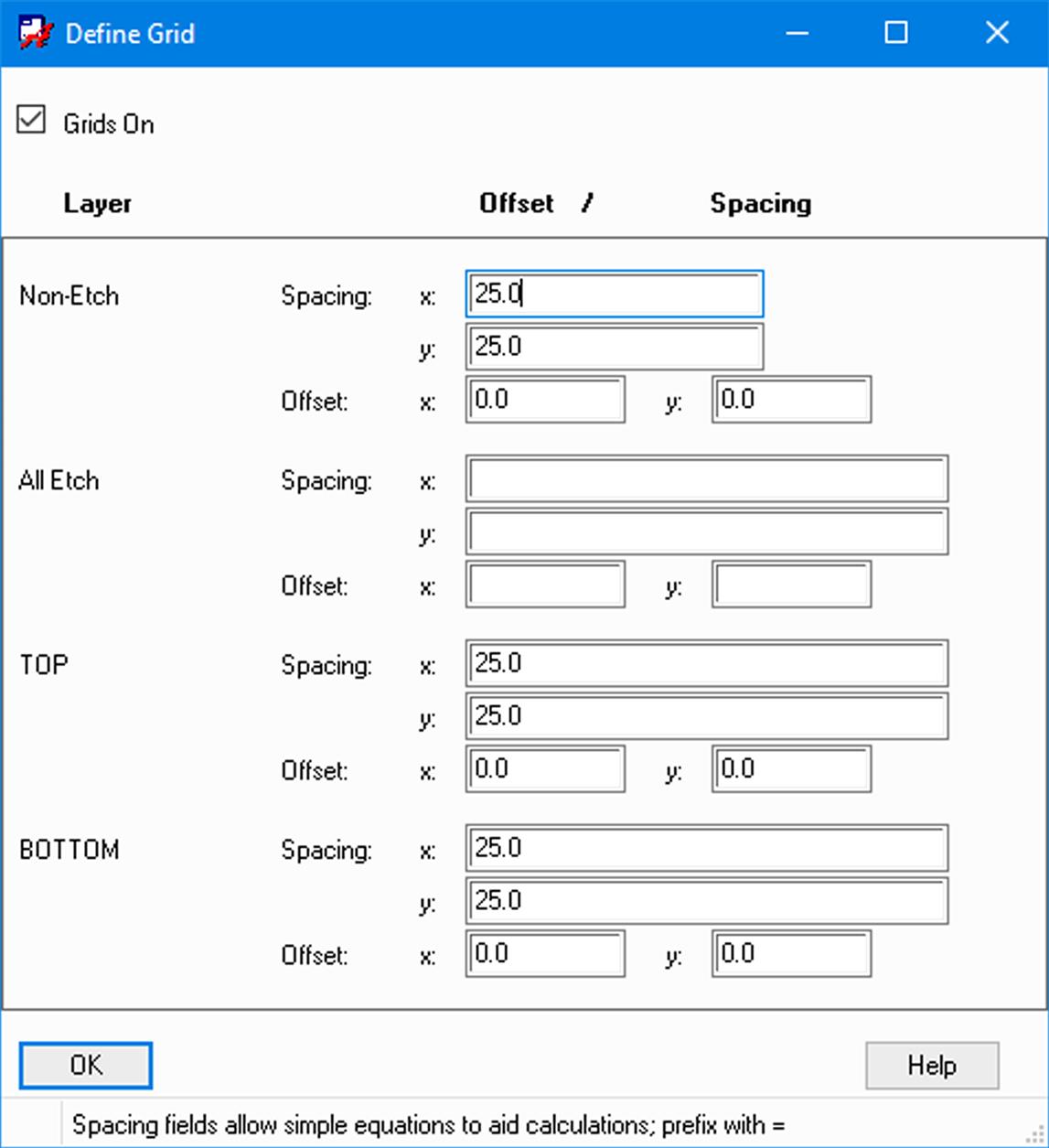
Select Other from the Size: list and enter the Extents values as shown in Fig. 8.12. Click Apply (but not OK yet). Select the Display tab. Enable the grid (if it is not already enabled) by checking the Grids on box and click the Setup grids… button to display the Define Grid dialog box shown in Fig. 8.13. For the time being set spacing for all of the layers to 25 mil. Entering values in the All Etch area will automatically change all the Top and Bottom values so that you do not have to set them individually. Click OK to dismiss the grid dialog box then click OK to dismiss the Design Parameters dialog box and update the work area.

The next step is to place the padstacks. Select Layout → Pins from the menu bar and in the Options pane press “…” after the Padstack: box to display the Select a padstack: dialog box as shown in Fig. 8.14.

Scroll down until you find the padstack that was just made. If it is not displayed, make sure the Database box is checked. If you did not make the new padstack, you can just pick one that is close in size; pad60cir42d is a good choice. Click OK.
A padstack will be attached to your mouse pointer. Place the first padstack by clicking and releasing your left mouse button at location (0, 0). Another padstack will be attached to your mouse pointer. Place the second padstack at location (400, 0) then right click and select Done from the pop-up menu.
Zoom in so that the two padstacks take up about 75% of your display (use your mouse wheel if you have one or use the Zoom Points button,  , on the toolbar).
 Zoom Points button
 Add line tool
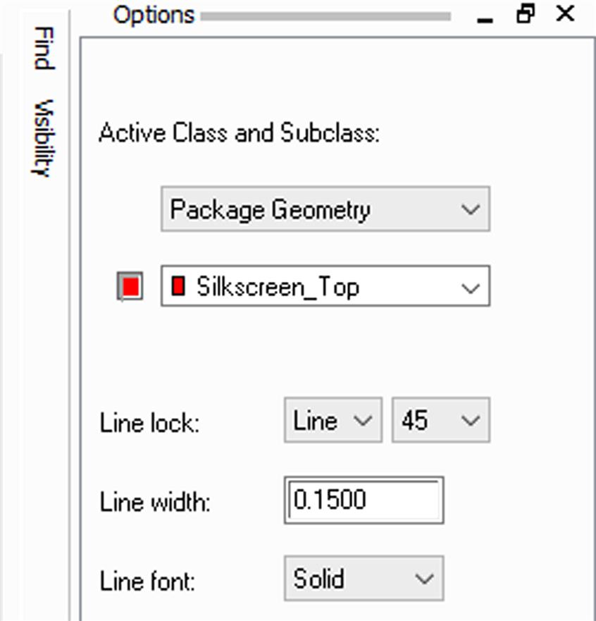
Next draw the body outline on the top silk-screen layer. To draw the silk screen, select the Add Line tool,  , select the Package Geometry class and Silkscreen_Top subclass from the Options pane, and select a Line width of 10 mil or so, as shown in Fig. 8.15.
Note: By default, lines (including rectangles) have a width of zero. When PCB Editor processes the artwork lines, those with a width of zero are ignored unless you specify a default width on the artwork control form. In addition, you can change the width of only lines, not rectangles. So if you want wide silk-screen lines, you need to use lines.
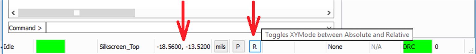
Begin the body outline by clicking and releasing the left mouse button at coordinate (75, −50). With the Add Line tool still active change the coordinates display from Absolute (A) to Relative (R) by toggling the small square XYMode button located at the lower middle of the screen (Fig. 8.16). Now move the pointer 100 mil in the Y direction (up) from the starting point (watch the mouse coordinates indicator at the bottom, the left arrow in Fig. 8.16) and left click and release to place a vertex. Move the mouse 250 mil to the right (X direction) and place another vertex. Move the mouse 100 mil down and place another vertex. Move the cursor back to the starting point, left click to place the last vertex, then right click, and select Done from the pop-up menu. The completed silk screen will be shown in white in Fig. 8.17.
 Color button
 Copy button
Note: To change the color of objects in the design, select the Color button,  , on the toolbar. Select the desired class from the left window, select the desired color from the color palette, and left click the colored square for the item you want to change in the subclass list at the right. Click the Apply button and then OK.
Next we add the body outline for the assembly layer by copying the silk-screen outline. To copy an object, select the Copy button,  , on the toolbar. Left click the silk-screen outline. Move the mouse up and away from the existing outline and left click to place the new outline. Right click and select Done from the pop-up menu to dismiss the Copy tool. The copy is on the silk-screen layer, so we change it to the assembly layer.
To change the layer of an object, select Edit → Change from the menu bar. Move the mouse over to the Options tab to display the pane, if is not already displayed. Select the Assembly_Top subclass under the Package Geometry class and change the line width to 1 (see Fig. 8.18). Left click on the copied body outline to make the changes. The outline will be changed but remain highlighted. Notice too that PCB Editor will tell you: Changed 1 items out of 1 items found, in the command window. Right click and select Done to complete the change.

 Move button
Move the new assembly outline to the same position as the silk-screen outline. To move an object, select the Move button,  , on the toolbar and left click the assembly outline; the outline will be attached to the pointer. Move the assembly outline over the silk-screen outline and left click to place it, right click, and select Done from the pop-up menu. The completed assembly outline will be shown in blue in Fig. 8.17.
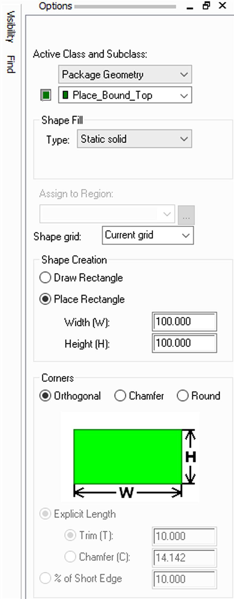
The next object to draw is the place boundary outline. Change the Non Etch grid spacing to 5 mil (Setup → Grids…). Choose Setup → Areas → Package Boundary from the menu bar, which will begin the outline as a static solid shape in the Package Geometry class and the Place_Bound_Top subclass as shown in Fig. 8.19.
Draw a box around the footprint so that the outline is as close to the padstack and detail objects as possible, while keeping them inside the place outline. The place outline will be shown in green in Fig. 8.17.
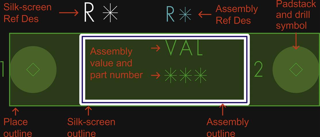
Now we add text objects to the footprint. Table 8.2 and Fig. 8.1 list some of the text objects that can be placed in a design, but as stated there, only one is required (i.e., at least one reference designator). See Fig. 8.17 while following the steps here. We begin by placing a reference designator on the silk-screen layer.
 RefDes button
To place a reference designator on the silk-screen layer, select the Label Refdes button,  , from the toolbar, or use Layout → Labels → RefDes menu. From the Options pane, select the Silkscreen_Top subclass (under the Ref Des class) and text block 2 for 31-mil high text (select a larger number for larger text). Left click above the place outline (off to the left a bit) to place the text marker. Type R* and then right click and select Done from the pop-up menu.
Controlling text size
The text block selection applies predefined text formats. To view or modify the formats, select Setup → Design Parameters from the menu bar and select the Text tab. Click the Setup Text Sizes button to display the Text Setup dialog box (shown in Fig. 8.20). From the dialog box, you can change the existing text formats or add your own custom text blocks.

 Add Text button
Next we place a couple of text objects on the assembly layer. Repeat the preceding process except select the Assembly_Top subclass and select text block 1. Left click above the place outline and to the right of the silk-screen reference designator. Again type R* and then right click and select Done from the pop-up menu. To add text object for the component value, select the Add Text button,  , from the toolbar, select the Component value class and the Assembly_Top subclass from the Options pane, and again select title block 1 if it is not selected. Left click below the reference designator on the assembly layer, type VAL, then right click, and select Done. Repeat this process to enter a part number label. Again use the Add Text tool but select the User Part Number class and the Assembly_Top subclass. Select title block 1 and type *, right click, and select Done.
The finished footprint is shown in Fig. 8.17. Save the footprint by selecting File → Save from the menu bar. PCB Editor will tell you Symbol ‘name.psm’ created in the command window.
That completes the first design example. You can compare this to the res400 symbol included in the native PCB Editor symbols library.
Example 2. Design of surface-mount device from an existing symbol
The native PCB Editor library contains one surface-mount capacitor footprint symbol and one surface-mount resistor symbol for general use. These capacitor and resistor footprints are roughly the 2010 and 1805 sizes, respectively. Many others are on the market. We could start from scratch and build our own; but since they are all similar, we start with an existing one and just modify it. In the next demonstration, we start with the existing smdcap footprint and modify it to make a size 1206 footprint.
Modifying an existing symbol: determining design requirements
Start PCB Editor and open the smdcap.dra located in the symbols library. Table 8.3 compares the smdcap symbol to the requirements of a 1206 chip capacitor as defined by IPC. Note that, since the origin is the body center, the outline coordinates will be ±1/2 the listed values.
Table 8.3
| smdCap | 1206 | |||
|---|---|---|---|---|
| Parameter | X | Y | X | Y |
| PAD size | 87 | 50 | 71 | 45 |
| PAD C/C | 195 | 118 | ||
| Body (L/W) | 245 | 90 | 126 | 63 |
| Place outline (L/W) | 250 | 90 | 185 | 91 |
| Padstack name | smd50_87 | smd45_71 | ||
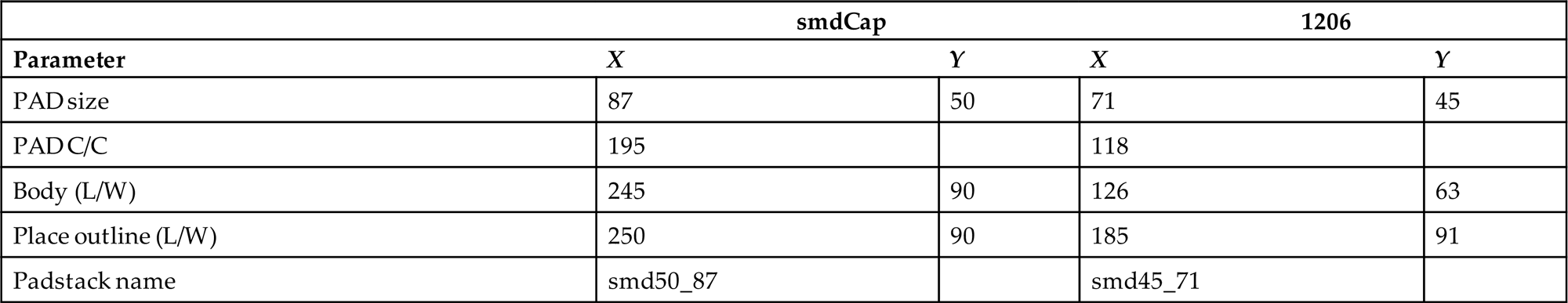
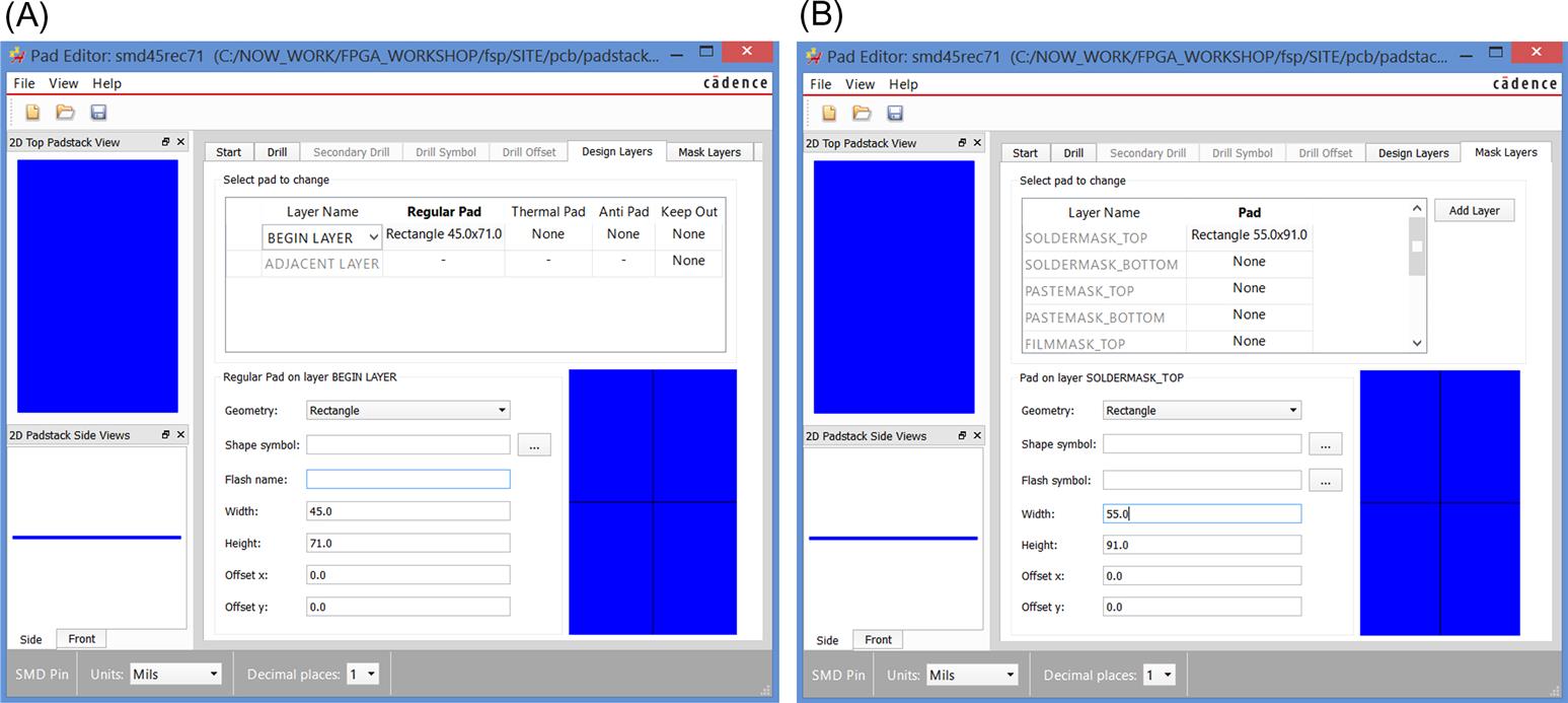
The closest equivalent padstack as defined in Table 8.3 for a size 1206 capacitor is smd44rec72. We use that as a starting point for a smd45rec71 padstack. Start Padstack Editor, open smd44rec72 and File - Save As… smd45rec71 in the symbols library. Since this is an smd padstack, you can leave the Start and Drill tabs alone, but select the Design Layers/Mask Layers tabs, and change top and soldermask dimensions as shown in Fig. 8.21A and B. Save your changes (File → Save from menu).
Replacing a padstack definition
Next we will change existing padstacks in the footprint drawing to the new smd45rec71 padstack.
Select Tools → Padstack → Replace from the menu bar. Select pin 1. At the Options pane, click the “…” button on the right of New: box to look for the new pad (Fig. 8.22).
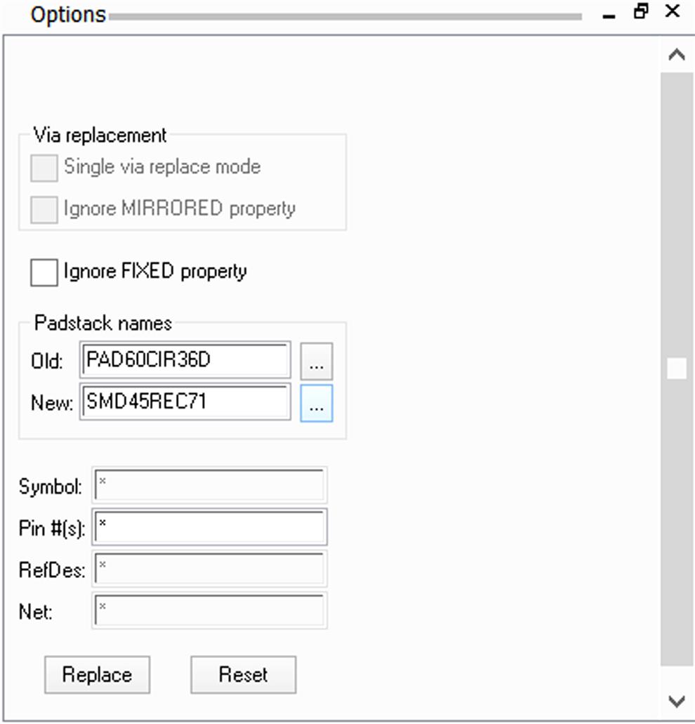
At the Select a Padstack dialog box, select the new one and click OK.
 Show Element button
At the Options pane, select a pin number or leave as * for all pins. Click the Replace button. The pads should be visibly different. To verify that the new pads are correct, select the Show Element button,  , and left-click on a pad. The information window will give you details about the padstack.
Next we need to move the padstacks. Set the grid to 1-mil-by-1-mil resolution (Setup → Grids…) and make sure XYMode is set to Absolute. Since pad center-to-center spacing is 118 mil, the left pad should be located at (−59, 0) and the right pad located at (59, 0). Use the Move tool and change the positions of the pads (turn off all other layers if it helps). Set the Find filter to Pins only if pins is unchecked. You can use P button in the status bar to pick the new location.
Next we need to modify the outline objects. Use Fig. 8.23 as a guide (which is based on IPC-7351B guidelines). When working with the outline objects, it can be helpful to change the layer colors and turn off all but the outline on which you are working. Otherwise you will need to use the right mouse button click and Reject menu to choose the required object for editing.

 Shape Select tool
We begin with the silk-screen outline. Turn off all layers except Package Geometry/Silkscreen_Top. To resize the outline, select the Shape Select tool,  , left click the object to select it. The line becomes dashed or highlighted, and square handles are displayed. Move your pointer over the outline, and it turns to a double-ended arrow. Use the double arrow to grab a line and slide it to the proper location. Do this on all the sides to produce the proper outline size.
As stated already you cannot change the width of the lines that make up rectangles. In some footprints, silk-screen outlines are made with lines and others (such as this one) are made with rectangles. Since the rectangles have an actual width of 0, they will be ignored during artwork generation unless you specify a default value for all zero width lines in the Undefined line width: entry in the Film Options area of the Artwork Control Form dialog box (opened from the Export → Gerber Parameters menu). In this example, thicker Lines were added to the rectangle to emphasize the silk-screen detail on the component sides. To do so, select the Add Line, change the line width to 10 mil in the Options pane, and draw lines on the component sides as shown in the figure.
Next manipulate the assembly outline using the procedure just described. The assembly detail shown in Fig. 8.23 is drawn so that it is the actual size of the component and additional lines are drawn to show the end caps and their relationship to the pads.
Don’t forget to change the size of the boundary shape in Package Geometry/Place_Bound_Top and/or Bottom subclass—this will be used during the placement process as the component boundary.
Finally, move the text objects as appropriate for the new symbol size. For viewability Fig. 8.23 does not show the assembly text objects.
Save the drawing and make sure that Symbol ‘smdcap1206.psm’ created is displayed in the command window, which completes the design example.
Example 3. PGA or BGA package design using the Symbol Wizard
Using the preceding procedures allows you to construct the exact footprint symbol you want, but for large or complicated footprints, there is an easier approach. To create the complex multipin packages, the OrCAD Library Builder option allows you to create IPC-7351B compatible packages, schematic symbols and 3D STEP models based on a set of predefined scalable templates. If you don’t have a license of OrCAD Library Builder, you still have a good basic Symbol Wizard in the OrCAD PCB Editor.
The Symbol Wizard performs many of the tasks automatically and can be used to create simple or complex footprint symbols. The resultant symbols contain all the necessary elements for a valid footprint symbol, but it may not meet your specific symbol requirements with regard to all the possible text and detail options. You can then use the procedures described in the second example to modify the automatically generated footprint symbol to meet your specific requirements. In this example the Symbol Wizard is used to construct a PGA footprint (Fig. 8.24) but you can easily create with it many other types of footprints such as DIP, SOIC, PLCC/QFP, discrete, SIP or ZIP.

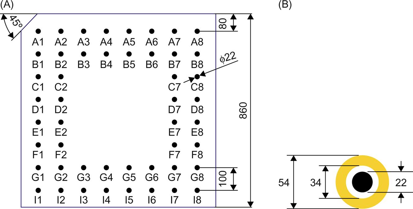
The Symbol Wizard is used in this example to construct a footprint for the PGA. The first step is to obtain a data sheet for the part. The dimensions for a generic 48-pin, 8×8 PGA are shown in Fig. 8.25, left. Each pin has a 22-mil diameter and is spaced 100 mil from the others. A padstack with a 32-mil hole and 50-mil-diameter pads suffices for the 22-mil pin (Fig. 8.25, right). Before starting the footprint design, you need to have the correct padstack present in the symbols library. A pad50cir32d padstack is included with the symbols library and is used for this design.
To begin the design process, open PCB Editor and select File → New… from the menu. At the New Drawing dialog box (Fig. 8.26), enter a name for the drawing (e.g., PGA_48pin) and select Package symbol (wizard) from the Drawing Type: list. Use the Browse… button to select a directory (the symbols library is default). Click OK to start the wizard.

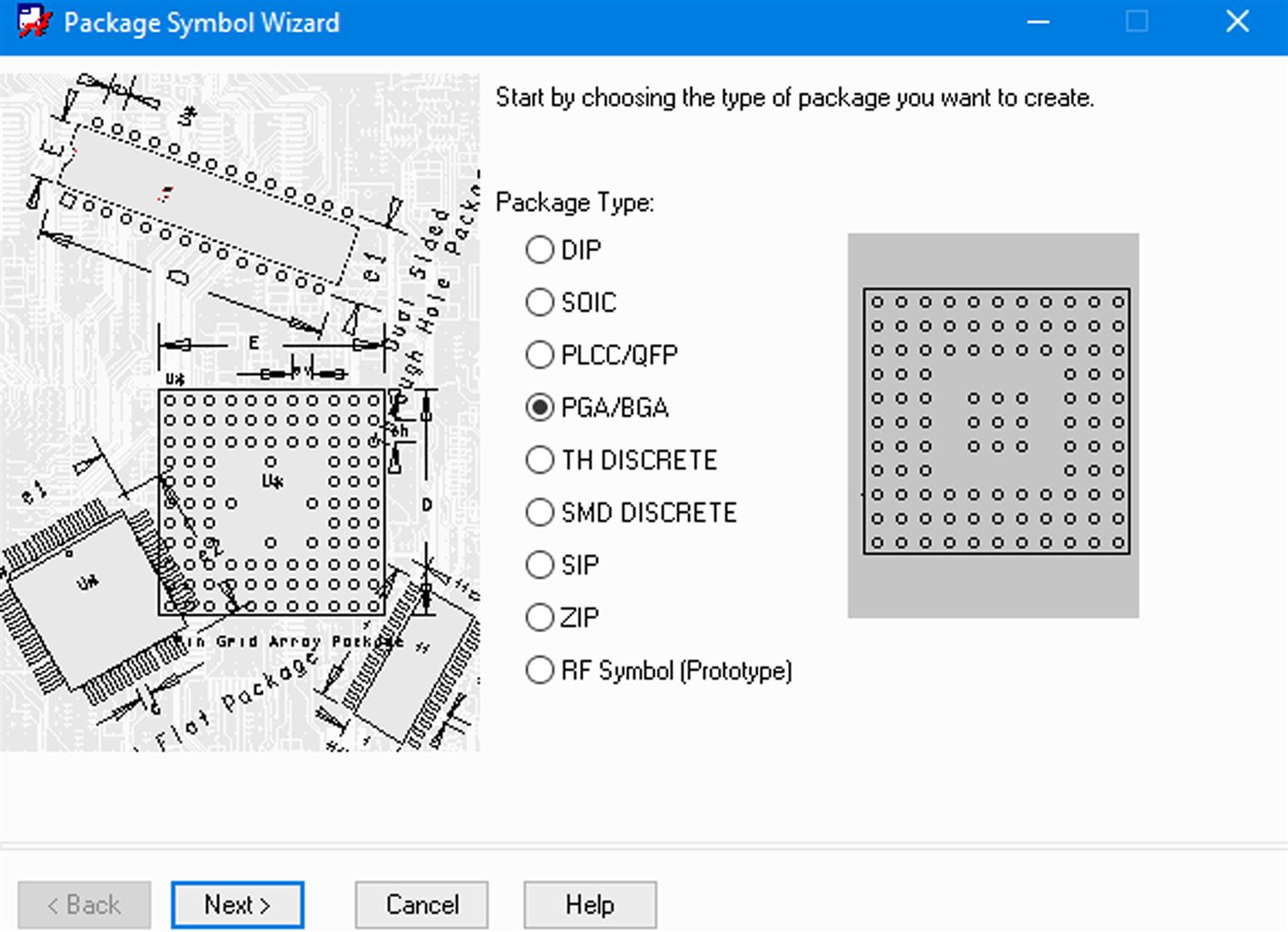
At the Package Symbol Wizard dialog box (Fig. 8.27), select the PGA/BGA radio button, and click Next>.
At the Template dialog box (Fig. 8.28), leave the Default Cadence supplied template radio button selected and click the Load Template button, then click Next>.

At the General Parameters dialog box, leave the default settings (mils) and click Next>.
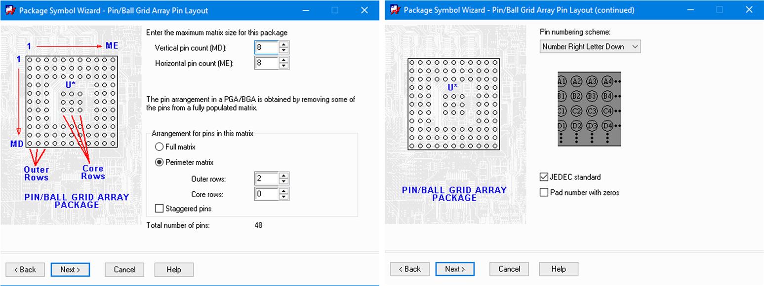
At the Pin Layout dialog box (Fig. 8.29), enter 8 for the vertical and horizontal pin counts. Select the Perimeter matrix radio button and enter 2 for Outer rows: and 0 for Core rows: as shown in the figure. The Total number of pins: should indicate 48, as required. Click Next>. At the next Pin Layout dialog box, leave the default settings (Number right and letter down and JEDEC standard). Click Next>.
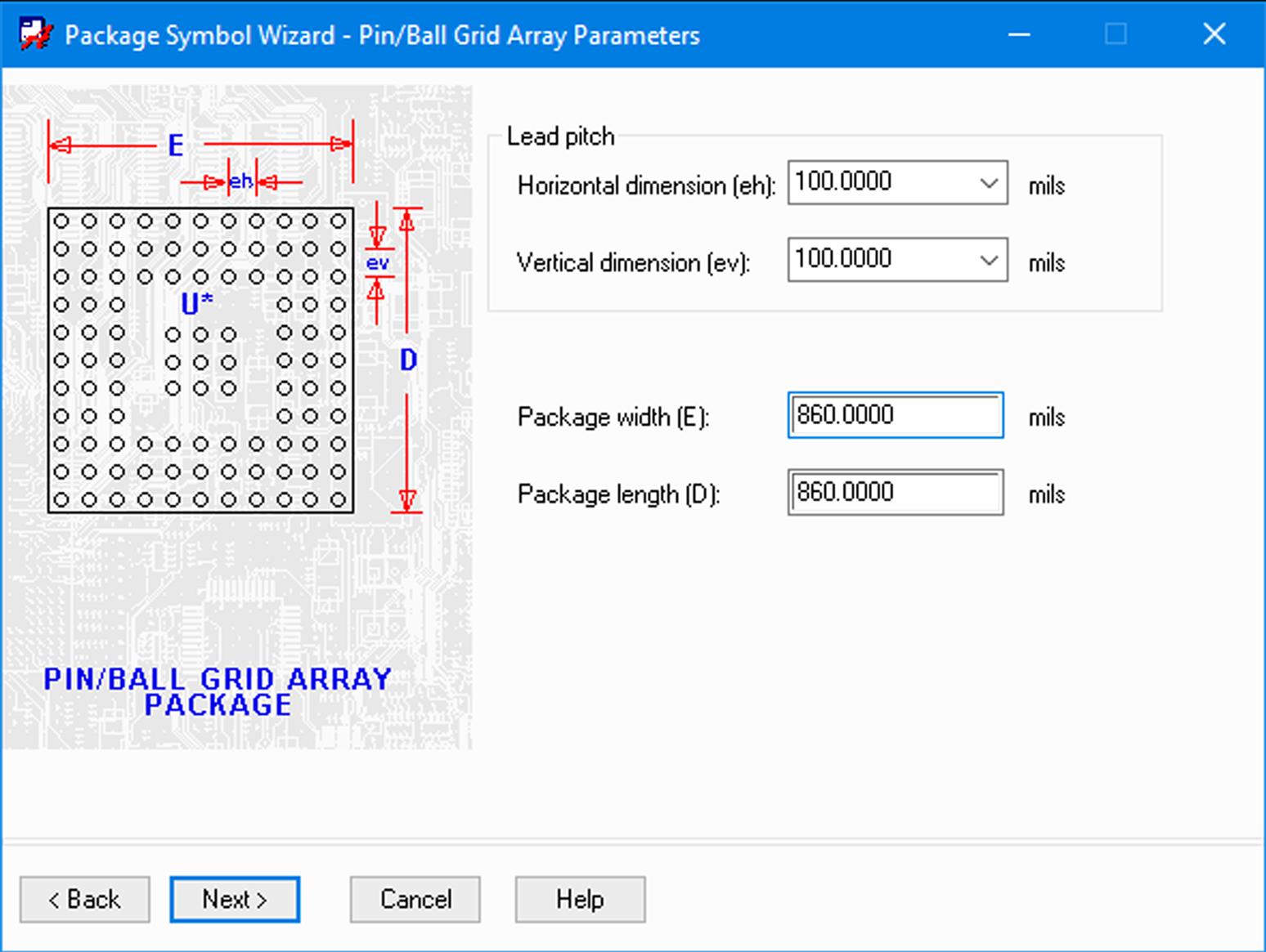
At the next Array Parameters dialog box (Fig. 8.30), leave the Lead pitch at 100 mil, but change the Package width and length to 860 mil, and click Next>.
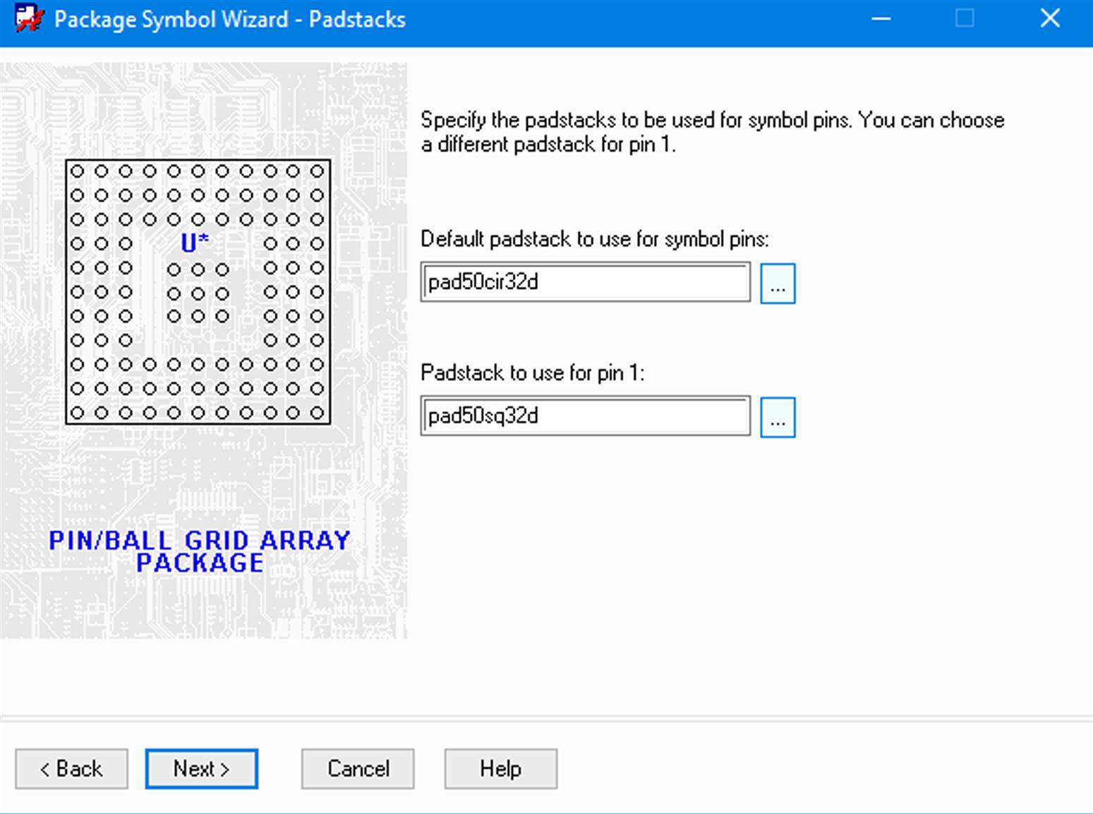
At the Padstacks dialog box (Fig. 8.31), click the Browse… button(s) and select pad50cir32d for the default padstack and pad50sq32d for the pin 1 padstack. Click Next>.
At the Symbol Compilation dialog box, leave the default settings and click Next>. At the Summary dialog box, click the Finish button to complete the design.
The new footprint symbol is shown in Fig. 8.32.

The new symbol contains Ref Des text objects on the Assembly_Top and Silkscreen_Top sublasses (Ref Des class) and four outline details on the Package Geometry class: Assembly_Top, Silkscreen_Top, Place_Bound_Top, and Dfa_Bound_Top subclasses (dfa stands for design for assembly). The place outlines are constructed of filled rectangles, and the silk-screen and assembly outlines are constructed of lines. All four outlines are shown as squares with zero width. We modify the outline objects to be more consistent with the IPC recommendations. Begin by changing the grid spacing to 10 mil (Setup → Grids…).
First, the Dfa_Bound_Top and the Place_Bound_Top outlines are expanded. Turn off the other outlines (use the Color button or the Options pane). Select the Select Shape tool as described previously. Left click on one of the place outline shapes to select it. Place your pointer over the outline and use the double-ended arrow to grab the outline edge. Drag the edge 40 mil outward from its current position. Do this for all four sides on both of the place outlines. When you are finished resizing the place outlines, turn them off and instead display the assembly top outline.
We now add a beveled corner to the assembly outline at the corner at pin 1, as shown in Fig. 8.33. Begin by zooming into the upper left corner of the symbol. Select the Add Line tool, at the Options pane select Package Geometry/Assembly_Top, and select Line and 45 as the Line Lock: options. Draw a diagonal line in the upper left corner as shown at (1) in Fig. 8.34.


Next we need to trim off the excess part of the outline. To do so, vertices need to be added so that they can be used as the trim points. To add a vertex to a line, select Edit → Vertex from the menu bar. Left click at the intersection of the diagonal line you just drew and the existing outline [points at (2) in the figure] and move the vertex out 20 mil or so to create an angle. Do this at each end of the new line.
Next delete the line segments [shown at the Xs near (3) in Fig. 8.34]. To delete part of a line segment disable any current tool (right click and select Done from the pop-up menu—if it is available; if it is not, no tools are selected). Check that the current application mode is General Edit. Hover your pointer over one of the line segments so that just the segment is dashed. Left click the segment to permanently select it. Select the Delete tool from the toolbar, and only the segment will be deleted. If you select the Delete tool first then select the line, the entire outline will be deleted. Finally, move the remaining line segments [the (4)s in the figure] back to the ends of the diagonal line (use the Vertex tool not the Move tool). Perform the same steps on the silk-screen outline and change the silk-screen outline width to 5 mil.
The only text objects added by the wizard were the Ref Des objects on the Assembly_Top and Silkscreen_Top subclasses. You can add your own as described in the preceding examples (e.g., value and part number on the assembly layer).
Select File → Save to save the drawing and update the .psm file. The completed footprint is shown in Fig. 8.33. To make the BGA instead of PGA you just need to replace the through hole pads to SMD pads.
Flash symbols for thermal reliefs
As described in Chapter 2, Introduction to the printed circuit board design flow by example, thermal reliefs are used to provide resistance to heat flow from a PTH to the copper plane to which it is connected during solder operations. Fig. 8.35 (left) shows how this is accomplished. A pad, belonging to a plated padstack, is connected to the larger plane through spokes. Between the spokes (and between the pad and the plane) are void areas where the copper is removed. The spokes provide electrical conductivity while the voids provide a barrier to heat flow. Flash symbols are used to define the voids on negative plane layers. Fig. 8.35 (right) shows the flash symbol in the negative image view and is described further.

Thermal relief connections between PTHs and copper areas on positive planes are automatically generated by PCB Editor so flash symbols need not be defined for positive layers. The ID (inside diameter) of the thermal relief is defined by the pad diameter from the Padstack definition in the Padstack Editor, while the OD (outside diameter) is defined by the ID plus twice the Shape to Pin definition in the Constraint Manager, either from the applicable Spacing Constraint Set where Nets are different, or from the Same Net Spacing Constraint Set domain where the Nets are the same. The spokes are generated in the board design by PCB Editor using trace width specifications defined in the Constraint Manager as is shown in the PCB Design Examples (Chapter 9).
Note that PCB Editor allows to define the plane layers as either positive or negative. Many old PCB projects used negative planes because they were efficient when computers were not as fast as today.
The realization of thermal reliefs on negative planes is another story. Recall that, with negative plane layers, what you see is what is removed, so thermal reliefs are generated by creating flash symbols (shown in Fig. 8.35, right), which define the void areas. Once a thermal flash symbol is attached to a padstack, PCB Editor interprets it and creates the positive view that you see with the “what you see is what you get” view presented during the board design. When manufacturing artwork is created during the last phase of a board design, the negative planes and flash symbols are properly processed as negative Gerber images.
Most of the padstacks in the symbols library have no flashes assigned to them. During the board design process, flashes need to be assigned to the padstacks as the need arises. When you construct your own footprints and padstacks, you can follow the same practice or assign flashes right away. Another useful application of the flash symbol is to define the array of openings in the solder paste (stencil) layer, when you want to split the big surface-mount technology pad to several small patterns to improve the soldering quality. Either way you need to know how to construct flash symbols.
A flash symbol is just another type of drawing you construct using PCB Editor. Later, a flash symbol is made for the padstack designed in the first example.
Before we begin with the drawing, we “engineer” the thermal relief. Recall from the first example that the padstack we designed (pad62cir42d) had the characteristics summarized in Table 8.4.
Table 8.4
Typically the flash’s ID (ID in Fig. 8.35, right) is the same as the regular pad for that layer, and flash’s OD (OD in Fig. 8.35, right) is the same as the antipad diameter plus or minus a couple of mils. The spoke width is calculated per IPC-2222A (pp. 21–22) and depends on the pad diameter and the number of spokes. The spoke width is calculated as
where W is the spoke width, P is the pad diameter, and n is the number of spokes.
If we assume that only internal layers have negative planes, then only the internal layers need a thermal flash. If it turns out that this is not the case, flashes can be added later.
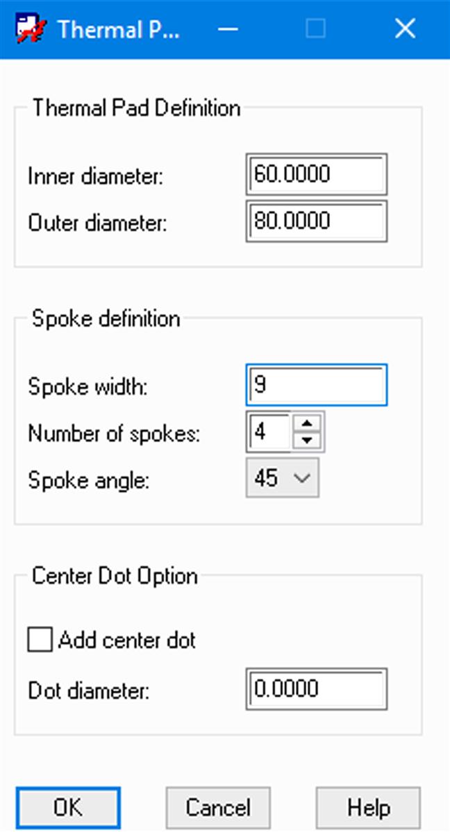
Then for the pad62cir42d padstack, the flash ID is 60 mil, the OD is 80 mil, and the spoke is 9 mil wide.
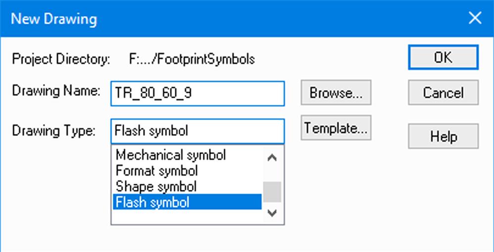
To construct a flash symbol, open PCB Editor. Start a new flash symbol drawing by selecting File → New… from the menu. At the New Drawing dialog box, enter a name for the symbol (e.g., TR_80_60_9 for thermal relief with OD=80 mil, ID=60 mil, and spoke width=9 mil), then select Flash symbol from the Drawing Type: list, as shown in Fig. 8.36. Click OK.
Turn on the grids and check to make sure that the origin coordinates (0, 0) are at the center of the drawing area. If not adjust the drawing area by giving the Left X and Lower Y Extents negative values (Setup → Design Parameters from menu, Design tab).
Next, select Add → Flash from the menu bar, as shown in Fig. 8.37.

As shown in Fig. 8.38, enter the design values for the pad diameters and spoke definitions into the Thermal Pad… dialog box, and click OK.
The completed symbol should look like Fig. 8.35 (right). Save the symbol (to symbols path) and make sure you see Symbol ‘tr_80_60_9.fsm’ created in the command window.
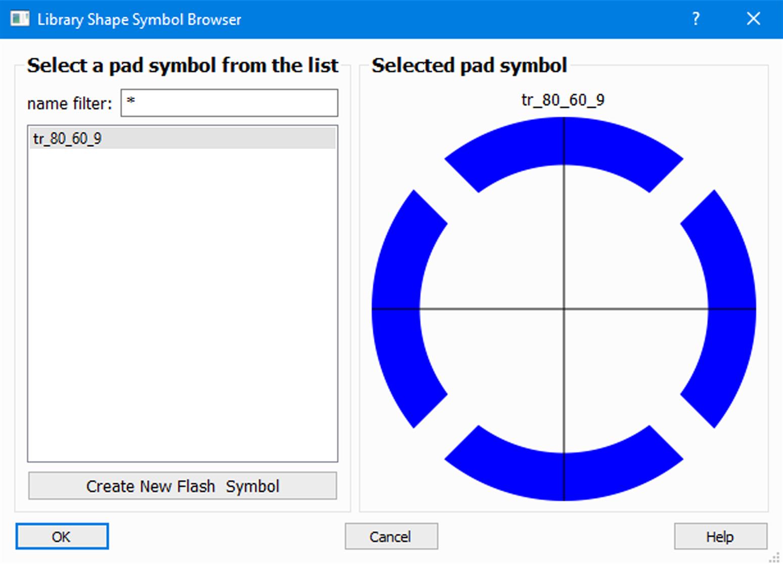
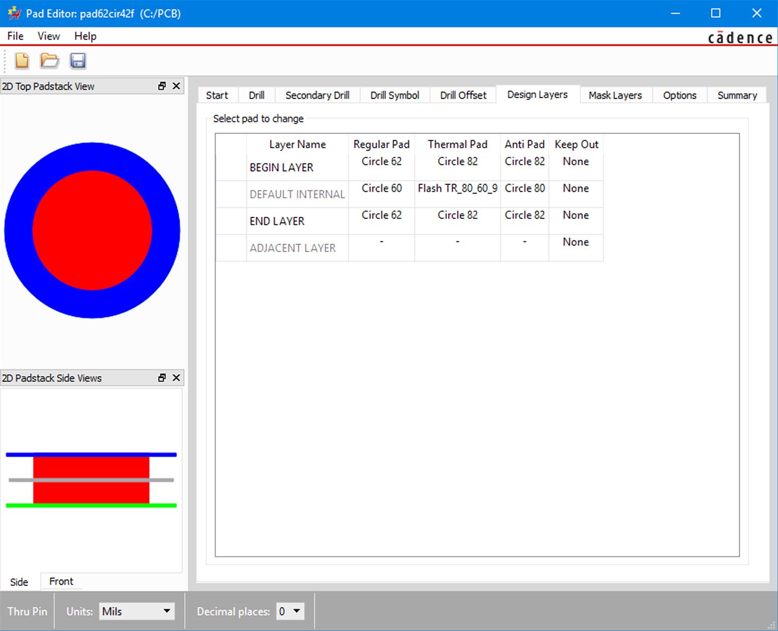
Now we can add this symbol to the pad62cir42d padstack definition. Use Padstack Editor to open pad62cir42d.pad again. Select the DEFAULT INTERNAL layer in the Design Layers tab. Click the Flash symbol: Browse… button,  , and from the Library Shape Symbol Browser dialog box (Fig. 8.39), select the Tr_80_60_9 flash symbol and click OK. Fig. 8.40 shows the flash symbol assigned to the padstack. Check that the Anti Pad in the DEFAULT INTERNAL layer is already defined as a circle with diameter=80, so that the pad shape for negative layer is defined for both connected, and not connected, pads on the negative plane(s). You can save the new definition with the same name or rename it to something like pad62cir42f to indicate that it has a flash symbol assigned to it.
You can now use this padstack definition in the footprint design you did in the first footprint design example. To do so, open the footprint drawing and change the padstack definition to pad62cir42f instead of pad62cir42d. Use the procedure in the second design example to change the padstack (Tools → Padstack → Replace…). This completes the flash symbol design example.
Mechanical symbols
Mechanical symbols represent physical objects you can place in your board design, which are not part of the netlist and therefore have no connectivity. They can be things such as mounting holes (mechanical pins without pin numbers), nonconnecting copper etch objects, design outlines, dimensions, and areas (e.g., keep-in and keep-out). Several mechanical symbols are located in the symbols library for you to look at for ideas. The mechanical symbols consists of two files which have the same file name and .dra/.bsm file extensions.
One important mechanical symbol that you may need to have is the mounting hole.
Mounting holes
Mounting holes can be used for attaching the PCB to mounting hardware (such as stand-offs) or for attaching hardware to the PCB (such as heat sinks). The four basic hole types are shown in Table 8.5; in them holes can be made with or without lands (pads), with or without plating, or in any combination of the two. Mounting holes that are plated can be attached to a net or isolated from all nets.
When mounting holes are attached to a net that is assigned to a plane layer, the mounting hole can be connected to the plane through thermal reliefs or with full contact, just like any other PTH. When mounting holes are attached to a net, they should be included on the schematic using a Capture part with an assigned footprint, which consists of a connection-type padstack. When mounting holes are not attached to a net, they are not included in the schematic and are added to the board design in PCB Editor. Some designers do not like to have connected mounting holes on the schematic, and it is possible to add them to the board in PCB Editor only. But it is the author’s opinion that this is a messy way to do it, since you have to override DRC errors to do it, and since it is connected to a net, it really is part of the circuit and should be on the schematic (if only for documentation purposes).
The PCB Editor contains several mounting-hole symbols, which have the name mtgXXX, where XXX indicates the hole diameter in mils. These are nonplated holes with no lands (without pads). The IPC standards call this an unsupported hole.
The mounting hole mtg125.dra is shown in Fig. 8.41. The drawing consists of a Pad125 padstack and a route keep-out area. The Pad125 padstack is a mechanical pin rather than a connect pin.

The mechanical pin properties are shown in Padstack Editor in Fig. 8.42. To view the pin launch, go to the Padstack Editor from PCB Editor by selecting Tools → Padstack → Modify Design Padstack… from the PCB Editor menu bar. Fig. 8.42 (left) shows the drill land plating settings in the Drill tab and Fig. 8.42 (right) shows the layers setting on the Design Layers tab.
The drill diameter is 125 mil, and the pads are 25 mil. This means that the pads will be drilled out during the manufacturing process. You will also notice that this is a nonplated hole, which means that this hole will be drilled toward the end of the manufacturing process, separately from the plated holes. A clearance (Anti Pad) is included and is 20 mil larger than the drill diameter, so that any copper planes are always kept away from the hole (this allows for fabrication tolerances).
Creating mechanical symbol drawings
To start a new mechanical symbol drawing, open PCB Editor and select File → New… from the menu bar. At the New Drawing dialog box, enter a name for the drawing and select Mechanical symbol from the list as shown in Fig. 8.43. Click OK.


You will be presented with a typical PCB Editor drawing window. Add lines, text, and dimensions as needed to complete your drawing.
 Add Pin button
To add mechanical pins, select Layout → Pins from the menu bar or select the Add Pin button,  , on the toolbar. Click the Padstack: Browse… button. At the Select a Padstack: dialog box, you can select any padstack or mounting hole you like. When you select a padstack and click OK in the dialog box then move your cursor to the drawing area, you will have the selected pin (padstack) attached to your pointer. Left click in the drawing to place the pin. Right click and select Done to quit. You can place an array or row of pins by entering X: and Y: Qty values in the Options pane. In that case, left click in the drawing area where you want the first pin located and PCB Editor will automatically place the remaining pins for you.
You can use the Padstack Editor to make the types of mounting holes shown in Table 8.5. A reference table of drill and screw sizes is provided in Appendix D as an aid to designing mounting holes for standard screw sizes.
For nonplated holes, select that option on the Drill tab. If you do not want pads on the hole, make the pad diameters smaller than the drill size. Remember though to make the antipads at least 20 mil larger than the drill diameter.
If you want to make a mounting hole that can be connected to a plane or net, the mounting hole will simply be a plated padstack. You can use them or design your own as described previously.
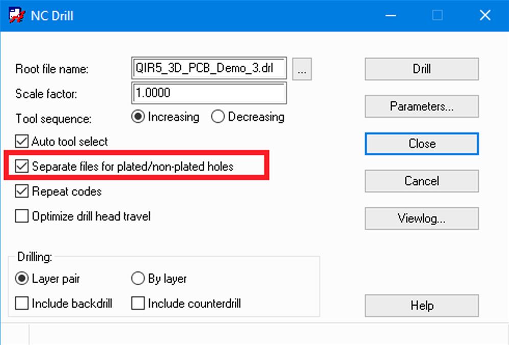
When a board design has both plated and nonplated holes, you can combine the drill information for both holes types into one NC drill file or have PCB Editor generate separate drill files. A second set of drill instructions is needed because nonplated holes are drilled after all plating processes are complete, whereas PTHs are drilled before the plating process; therefore a completely separate set of instructions is required.
The standard, plated drill file has the naming convention name.drl file, and nonplated drill files have a name-np.drl naming convention. You specify combined or separate drill files by selecting Manufacture → NC → NC Drill… from the menu bar. At the NC Drill dialog box (shown in Fig. 8.45), uncheck the Separate Files option to generate a combined drill file for all types or select the option to make separate files.
Placing mechanical symbols on a board design
Examples of how to place a mounting hole (a mechanical symbol) on a board are given in Chapter 10, Artwork development and board fabrication, and Example 2 of the Chapter 9, PCB Design Examples. Open your board design and select Place → Mechanical Symbols... from the menu bar to display the Placement dialog box, as shown in Fig. 8.46. Make sure that both the Library and Database options are checked in the Advanced Settings tab and press the “+” icon to open the list of available mechanical symbols in the library. Check the box next to the symbol you want and left click on the board area at the desired location to place the mechanical symbol. Repeat the process for each symbol you want placed on your board.

Blind, buried, and microvias
Blind and buried vias are not typically designed into footprints but are added to a PCB during the layout and routing process. Example of PCB design using blind vias is given in the Chapter 9, PCB Design Examples (Example 3), but is discussed briefly here since it is related to padstack design.
Fig. 8.47 shows how microvias and blind and buried vias can help route high-density ball grid arrays (BGAs). Using these via types, a BGA can be placed on the top of a board and another SMD can be placed directly opposite the BGA on the bottom of the board. To accomplish this, typical through-hole vias cannot be used. Fan-out and routing of the BGA are accomplished using blind and buried vias. Blind vias are visible on only one side of the PCB and connect traces on the one outer layer to inner traces only, while buried vias are not visible from either side of the board and connect traces only between inner layers.

Blind and buried vias are realized on built-up PCBs. A built-up PCB often has a standard layer stack-up core [section (a) in Fig. 8.47] and additional layers are sequentially added to the board [the two (e) sections in Fig. 8.47]. PTH vias in the standard core become buried vias [(b) in Fig. 8.47]. As the outer layers are built up on top of the base core, buried microvias [(c) in Fig. 8.47] and blind microvias [(d) in Fig. 8.47] can be embedded into the outer layers. During the build-up process, resistors or capacitors can also be buried in the layers. After all the layers have been built up, additional microvias [(f) and (g) in Fig. 8.47] and standard PTHs [(h) in Fig. 8.47, tented on the top end] can be added to the entire assembly.
Fig. 8.47 shows three types of microvias: (c) and (g) are laser-drilled, plated vias; (d) is a laser-drilled, paste-filled via; and (f) is a plasma-etched, plated via. To learn more about designing built-up boards and microvias, see Coombs’ Printed Circuits Handbook (Coombs, 2001).
Blind and buried vias can be constructed in three ways. One way is to use Padstack Editor to design the via padstack directly. In general, you use the Padstack Editor the same as was described for the normal through-hole padstacks. If you know exactly what the layer stack-up definition will be in your board design, you can add those layers to a padstack definition in Padstack Editor and remove other layers. In Padstack Editor, select BBVia or Microvia on the Start tab. On the Design Layers tab, add and name layers to the stack-up as needed. To add layers to the stack-up, right click on the layer that will be below the one you are adding and select Insert from the pop-up menu. Give the new layer the name used in your board design and select the appropriate pad sizes. For all other layers, select Null for the pad values. An example of a blind via design is shown in Fig. 8.48.
The second way is to set up vias interactively from the board design using the BBvia tool. This is the easiest way to make a blind or buried via, because all the layer definitions are already set up in the board design (using the Layout Cross Section dialog box) and will be known to the BBvia tool. The BBvia tool is launched by selecting Setup → Define B/B Vias... from the menu, as shown in Fig. 8.49. As indicated in the figure, two options are available.

If you select Define B/B vias…, you get the dialog box shown in Fig. 8.50. This method creates one padstack that goes from the Start Layer to the End Layer and includes all the layers between them.

If you select Auto Define B/B vias…, then you get the dialog box shown in Fig. 8.51. You can select which layers will be used in setting up the via. This method actually makes several vias. Essentially, it makes as many blind and buried vias as necessary to connect each of the adjacent planes (two layers at a time) and to connect the start and end layers to each other and to each of the internal layers. Which vias get used in the board design is controlled by the Constraint Manager in PCB Editor as demonstrated in the PCB Design Examples (Chapter 9).

OrCAD Library Builder
The OrCAD Library Builder is a tool that allows to generate semiautomatically the schematic symbol, footprint, and 3D model in accordance to IPC-7351B standard. It offers a lot of templates for many typical packages, such as small outline integrated circuit, thin quad flat package, quad flat no leads package, and BGA, which can be scaled to the needed number of pins, pitch, and size of the package. Also it allows to extract the pin table from the data sheet in Adobe PDF format. In order to use it, you need the appropriate license.
3D canvas
The 3D viewer embedded to OrCAD PCB Editor supports the use of 3D models of the components in STEP format (files *.stp or *.step). It displays the bare PCB with all holes, traces, and pads, the PCB with components and mechanical items, including the enclosure, if its 3D model is attached to the project as a mechanical symbol. In order to attach the STEP model to the footprint or mechanical symbol, you can use Setup → Step Package Mapping... menu during creation of the footprint or mechanical symbol, or directly in the PCB project. The *.STEP files should be located in the appropriate library path (STEPPATH) which is set in PCB Editor User Preferences. Also it’s possible to view in 3D only the selected group of objects, for example, single net routing.
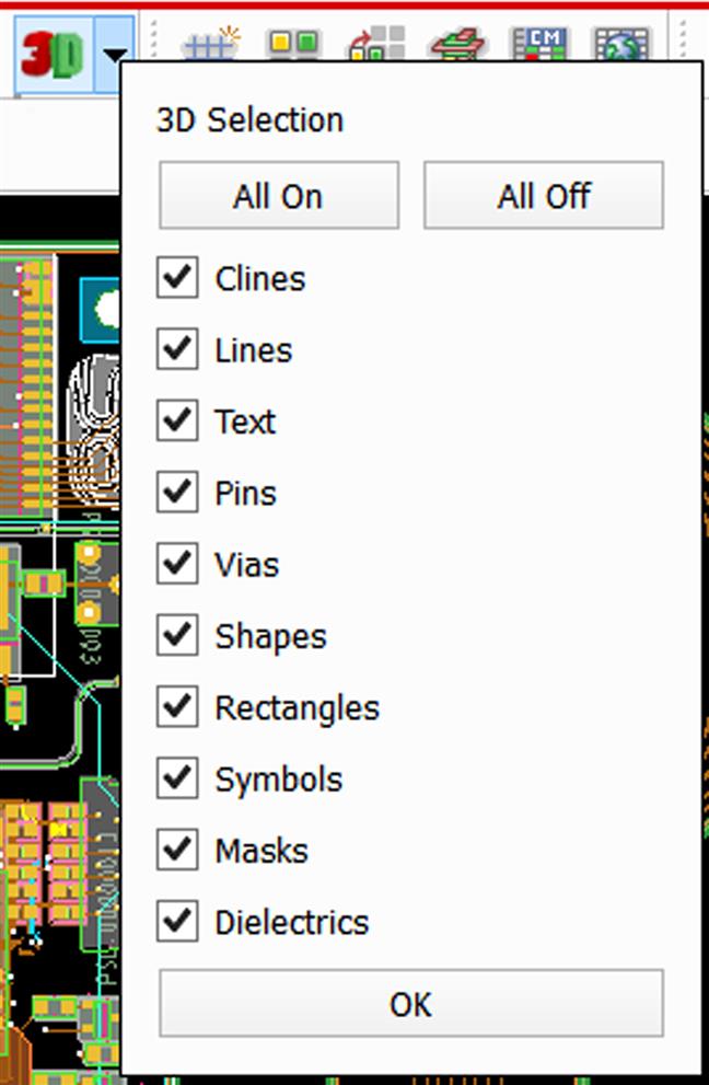
You can run the 3D viewer via the Display → 3D Canvas menu option or the 3D icon. It’s possible to tune the set of the objects which you want to see, by clicking the black triangle located near the 3D icon (see Fig. 8.52).
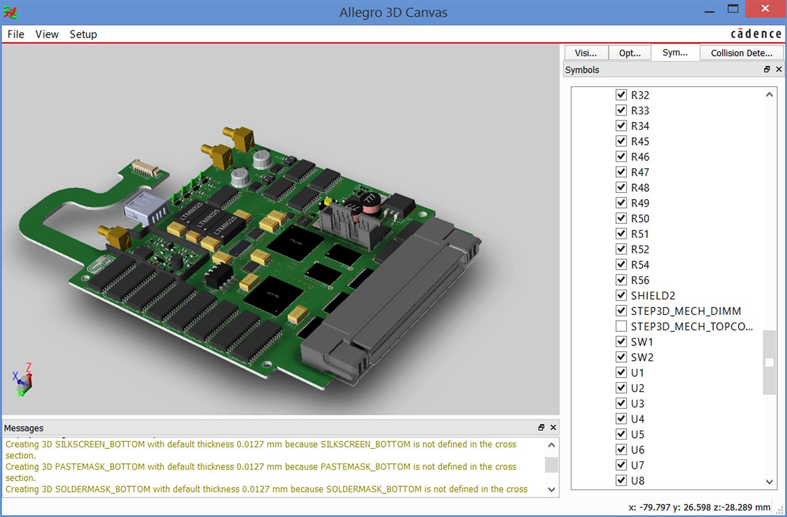
The 3D canvas is shown at Fig. 8.53. Zooming is controlled by rolling the mouse wheel, panning is controlled by pressing the mouse wheel (middle-click) then dragging the mouse, rotating is controlled by holding the Shift key while pressing the mouse wheel then dragging the mouse. The File menu contains the following choices: Export, Output, and Close. The View menu allows to change the view direction, and to control the visibility of different panes of the viewer. The Setup menu allows to set the Preferences, such as colors and cutting plane. The Control panel on the right contains several tabs that allow to control the canvas: Visibility, Options, Symbols, and Collision Detection.
The Export menu allows to export the 3D model of the whole PCB with components to such formats as STEP, ACIS, HMF, HSF, IGES, PDF 2D, PDF 3D, and some others. The exported STEP 3D model can contain the dielectric layers and copper topology with the proper thickness of every layer, according to the PCB stack-up.
The Output menu sets the output file and path for messages (the log file). The Close menu will close the 3D canvas.
The Visibility tab is similar to the Visibility tab in PCB Editor. It allows to turn on or off the different layers and objects in 3D view.
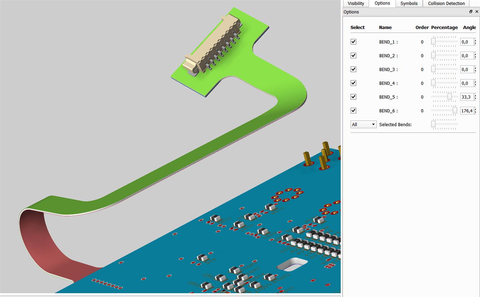
The Options tab allows to enter the options for the active pop-up command, which can be activated by the right mouse click on the canvas. The available commands are: Move, Bend, and Measure path.
With the Symbols tab user can control individually the visibility of any component on TOP and BOTTOM side of PCB, as well as the device case and mechanical parts. To open the list of components you should click on the “>” sign on the left of “All,” “TOP,” or “BOTTOM” folder.
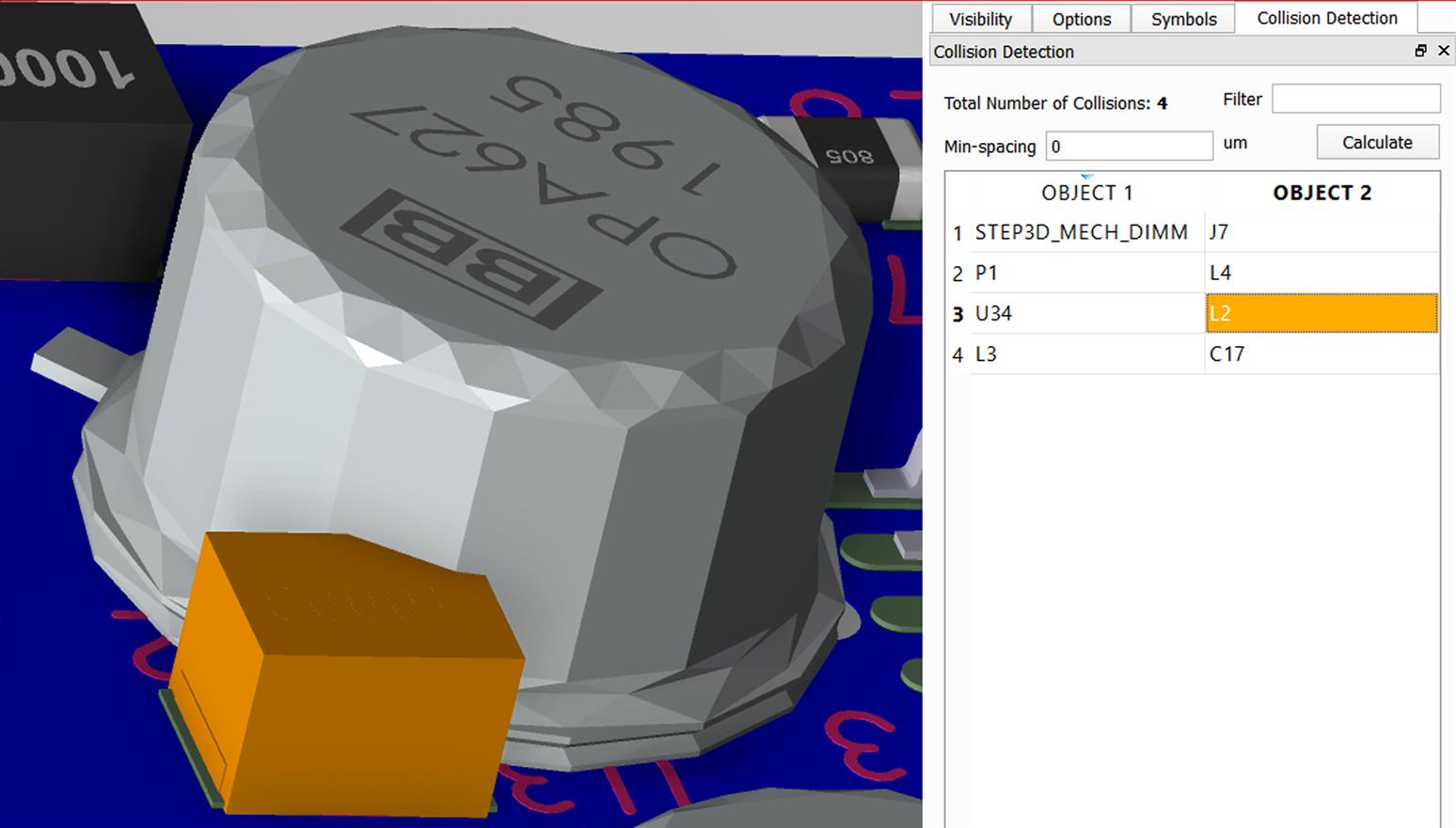
The Collision Detection tab is a very powerful tool to check any touching of surfaces of different components, or of the component to the rigid or flexible part of the PCB or some mechanical detail. To run the check, enter the Min-spacing value, for example, 0.1 mm, and push the Calculate button. After few seconds, you will see the list of detected collisions as the pairs of component names. A left-click on the name will highlight the component (Fig. 8.54), you can also right click on the name and choose Locate to make the component blink in the canvas.
The Messages window displays all messages from 3D canvas. You can stop displaying of new messages by checking the Silent mode checkbox in the Messages category of the Allegro 3D Canvas Preferences dialog.
If you wish to review the messages later, use File → Output → Messages menu option to save them to a text file.
The messages in 3D canvas follow a special color scheme to easily detect their type:
Messages displayed in red are errors; Messages displayed in pale yellow are warnings; Messages displayed in black are information.
Bending the rigid-flex printed circuit board in 3D canvas
A right click in the canvas will show a pop-up menu with three options: Move, Bend, and Measure Path. If Bend is selected, you will see the options for the command in the Options tab. Use the sliders to bend the selected or all bending areas (see Fig. 8.55). To enable bending of the flexible sections, first setup several stack-up zones in PCB Editor, then create the bend areas using menu Setup → Bend → Create, and finally set the anchor for 3D bending with the menu option Setup → Anchor 3D View (otherwise the Bend menu will be grayed out). It is possible to combine the bending and collision detection tools to detect collisions when flexible sections of the PCB have bends applied.