
Adding Ground Planes and guard traces to Routing layers
As discussed at the beginning of these examples and in Chapter 6, Printed circuit board design for signal integrity, you can reduce noise levels on signal lines by surrounding traces with copper planes and guard traces. Not everyone agrees with this practice, but it is demonstrated here in the interest of completeness. The following procedures demonstrate how to use the Add Connect tool to add ground nets and use shapes to add copper planes to Routing layers.
Routing guard traces and rings
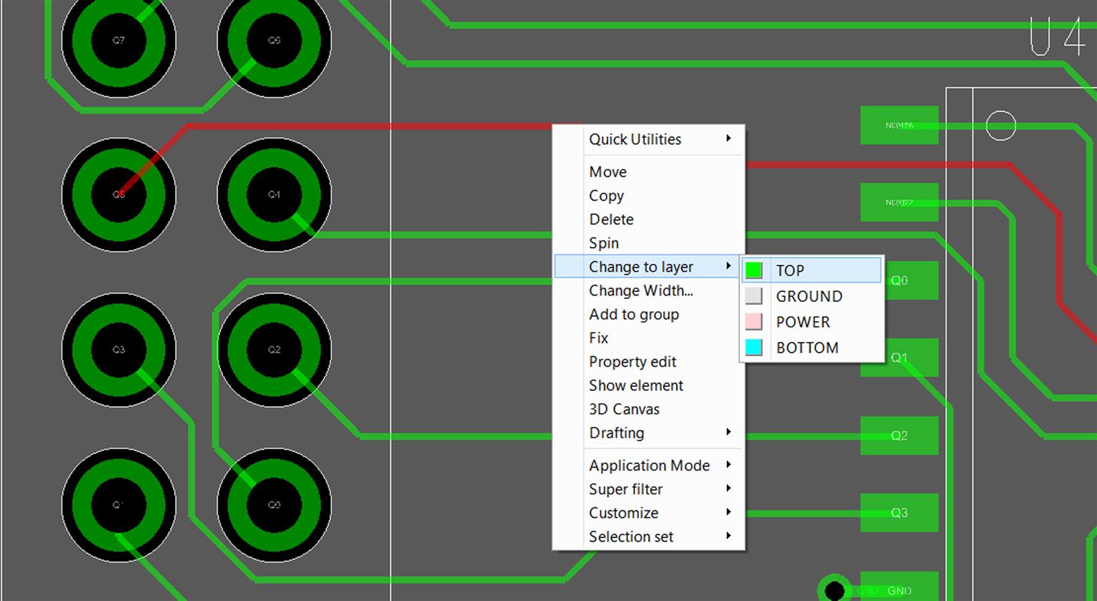
If you have one or two traces that could have cross-talk problems, you can add guard traces between them that can be attached to the Ground plane with vias. You can also add guard rings around component pins. Like the guard traces, the guard rings are attached to the Ground plane with vias. It should be noted though that their usefulness is debated in the literature, because they can cause more problems than they fix if not applied correctly (see Appendix E for references). Fig. 9.107 shows examples of guard traces between the control and the data lines and guard rings around one of the microcontroller pins.
To place guard traces that are attached to the Ground plane, select the Ground plane on the Options tab and select the Add Connect tool. Left click on the Ground plane where you want to begin the guard trace. Right click and select Add Via from the pop-up menu. The Add Connect tool should still be active, and you should now be on the Top layer (but check the Options tab to make sure). Draw the trace where you want the guards to be. At the end of the trace, left click to finish the trace then right click and select Add Via. At various intervals along the trace, add vias to securely stitch the guard trace to the ground plane. To add the vias, select the Add Connect tool, left click on the trace where you want the via, right click and select Add Via. Repeat this where ever a via is needed.
To add a guard ring around a component pin:
- 1. Select Shape → Circular.
- 2. Right click over the pin.
- 3. Choose Snap pick to → Pin from the pop-up menu (Fig. 9.108A).
- 4. Draw the round shape connected to GND net, and left click to finish the shape (Fig. 9.108B).
- 5. To create the void in it, select Shape → Manual Isolation/Cavity → Circular (Fig. 9.108C).
- 6. Left click on the recently created shape to select it. It should become highlighted.
- 7. To select the pin as the center of the created void right click over the pin and choose Snap pick to → Pin from the pop-up menu, and draw the void around the pin. Left click to finish the void.
- 8. Select Route → Connect to create the via that will connect the guard ring to the GND plane (Fig. 9.108D).

It’s also possible to add the arrays of vias around the object using the tool Place→Via arrays→Boundary. If you use this tool, you should set up the parameters in the Options pane:
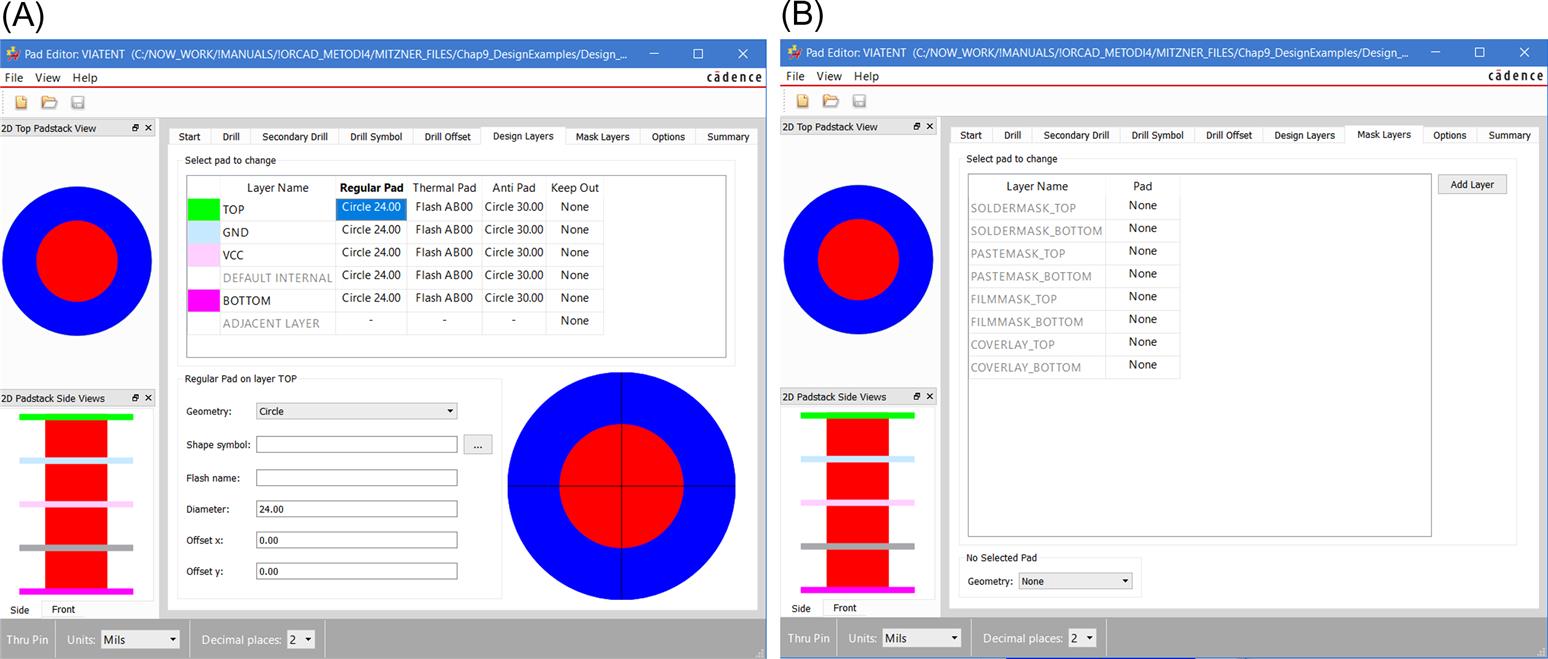
Adding Ground planes to Routing layers
Next we add Ground planes to the top and bottom Routing layers. To add Ground plane areas to a Routing layer, make the Top (or Bottom) Etch layer active and select either the Shape Add button,  , or the Shape Add Rect button,
  . Display the Options tab and select Dynamic copper and assign the GND net to the shape, as shown in Fig. 9.109.

An example of a copper plane is shown in Fig. 9.110. Notice that thermal reliefs are automatically placed on pins and pads. The spacing of the plane to the pad (pin) and the spoke width are set using the rules in the Constraint Manager.

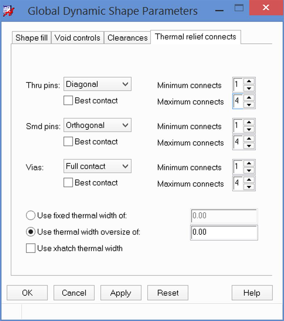
Thermal reliefs are set to orthogonal (+) by default, but you can change them to diagonal (×) if you prefer. To change the direction of thermal reliefs on a positive Plane (Routing) layer, select Shape → Global Dynamic Parameters from the menu bar. In the Global Dynamic Shape Parameters dialog box (see Fig. 9.111), select the Thermal relief connects tab and choose the desired direction.
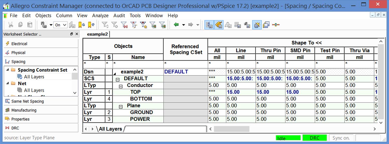
To change the spacing of the Ground plane to pins on a Routing layer, launch the Constraint Manager and select the Spacing tab (Fig. 9.112). Select the Shape to section in the Spacing Constraint Set folder and select the TOP layer row (or whichever layer you want to change) in the DEFAULT spacing CSet. Change the Shape to Line, Shape to Thru Pin, or even Shape to All, and so forth settings to the desired width. Changes are effective immediately; however, if your plane areas were not drawn using dynamic copper, your design may look as if something has gone horribly wrong.
If the ground plane on the Top layer suddenly takes over, the design is actually OK, the shapes just need to be updated. To update the Ground plane shape, select Check → Design Status from the menu bar. In the Status dialog box (Fig. 9.113), select the Update to Smooth button. The Ground plane should now look correct again and have the proper spacing.

You can enable the immediate update of Shapes to the Smooth state by setting the Smooth radio button in Shape → Global dynamic parameters → Shape Fill.
To change the spoke width of thermal reliefs on a Routing layer, select the Physical tab in the Constraint Manager (see Fig. 9.114). Select the All Layers icon under the Net folder. Change the line width of the net that has the thermal reliefs you are interested in. The spokes and traces will now be the same for the nets you modify. Perform the Update Shapes step as described previously to update your board design. If you need to have certain trace widths for specific segments on a net and you do not want to have these changes affect them, you must go back and change those segments back to the way you want them using the Change Objects command (in the Edit menu) and the Options and Find filter tabs. Once the changes have been made, you can then Fix them so that the changes are not undone.

Once your plane is established, remember to place voids and merge copper areas and the like on the new plane to match the inner Ground plane as appropriate. Update the DRC to make sure the copper pour did not cause any errors.
You can add a Ground plane to the Bottom layer (or any other Routing layer for that matter) using the same procedures used for the Top layer. When you have several Ground planes, it is important that they have many low-impedance connections to help keep the planes at the same potential throughout the board area. This is done by placing vias, which are connected to the net for those planes, at various places. These vias are sometimes called stitching vias. To place stitching vias on a board to connect multilayer Ground planes, select the Add Connect tool, left click on the plane that needs the via (a trace will be started), right click and select Add Via from the pop-up menu. To place multiple vias, use the Copy button, with checked Vias in the Find filter pane to copy the via and left click wherever you want a via placed (right click and select Done to quit). An example is shown in Fig. 9.115. It is also a good idea to place a couple of vias underneath the ADC (U2). To add the array of stitching vias, you can also use the Place → Via Arrays → Matrix tool.

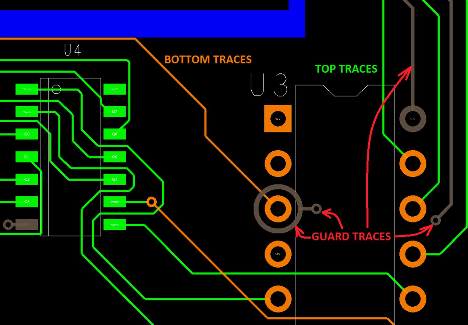
If you look closely at the ground strips between some of the traces and between some of the pins on the connector, J1, in Fig. 9.110, you will notice that some areas are isolated from the rest of the Ground plane. These isolated strips are called islands. Islands can act like antennas, which can pick up high-frequency noise (EMI) and cause problems for the rest of the circuit. To solve this problem, the strips and islands need to be either tacked down to the Ground planes using the stitching vias, trimmed, or removed altogether.
Use vias as just described to tack the strips to the underlying Ground plane. For parts of strips or islands that you want to trim from larger, stitched sections, use one of the Shape Void tools to remove unwanted sections of the strip. To trim islands and isolated strips, select one of the Shape Void tools and use the Options tab to select the correct layer and net to void. Select the shape, then draw the void shape over the area you want removed.
To completely remove strips or islands, use the Island_Delete tool,  , or select Shape → Delete Unconnected Copper. By default all islands on a layer associated with a particular net will be deleted. Use the Options tab to select whether to delete all the islands on that layer or just specific ones. To delete only specific islands, select the First button on the Options tab then left click on the island you want to delete. Right click and select Done when finished.
This completes Design Example 2.
Example 3. Multipage, multipower, and multiground mixed A/D printed circuit board design with PSpice
Introduction
Multipage schematics can be used to organize and simplify large circuit designs and to incorporate PSpice simulations prior to laying out the board design. The mixed analog/digital circuit from the last example (see the schematic in Fig. 9.90) is reused in this example but is modified to demonstrate how to route a single PCB from a multipage schematic project and add PSpice simulation capabilities. The example also demonstrates two methods used to establish isolated Ground planes using blind vias and a buried chassis shield. The technique allows quiet circuits to be placed on one side of the board and shielded from noisy digital circuits, which are placed on the other side of the board.
Multiplane layer methodologies
In the previous example, a single Plane layer was used to produce a digital ground and an analog ground even though there was really only one ground net. The two ground systems were produced by physically segregating the parts on the board and removing a strip of copper from the one plane (creating a split plane) between the two circuit areas.
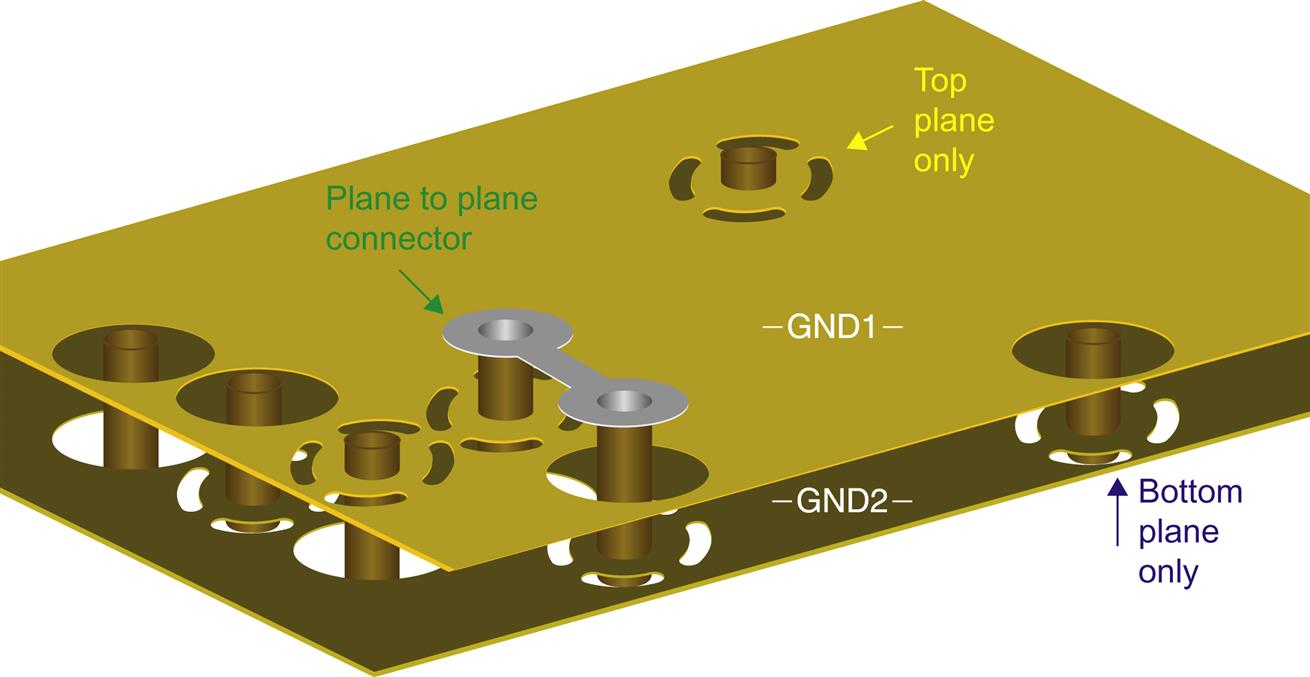
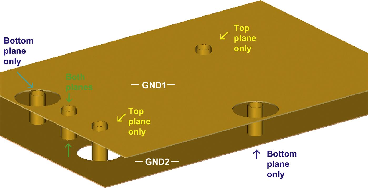
In high-density, high-frequency digital designs, multiple Ground planes are often used even when there is only one type of circuit ground (as demonstrated in Example 4). This helps reduce loop inductance when using multiple Routing layers and control trace impedance (see Chapter 6: Printed circuit board design for signal integrity, for details). When two Plane layers are used for a single ground net, connections are made to both planes simultaneously via plated through holes (whether for through-hole leads or fan-outs from SMDs) anytime a connection is made to the net. This is shown in Fig. 9.116.

In this example, continuous Plane layers are desired for both the analog and the digital parts of the circuit. As described in Chapter 6, Printed circuit board design for signal integrity, significant cross talk can occur between adjacent planes if there is any overlap between the two plane areas. Since both the analog and digital planes extend out to the limits of the board, there is complete overlap. One way to minimize cross talk is to insert a shield between them that carries no signal currents.
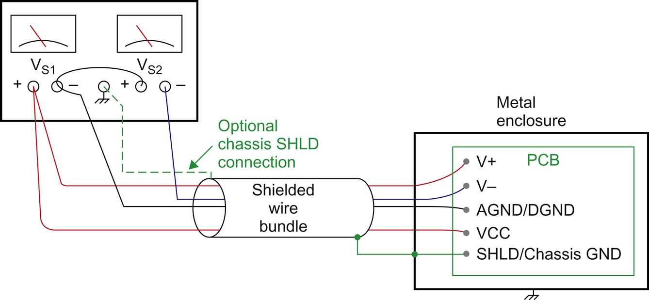
Fig. 9.117 shows the system design concept for this example. This is just one of many possible types of PCB power distribution schemes. The system uses a dual power supply for ± analog power for op amps and a single power supply (VCC) for digital circuits. The analog and digital systems each has its own ground system on the PCB; however, a common reference voltage is required for the ADC. To facilitate both requirements the grounds are tied together at a single point on the PCB before returning to the power supply. To keep the two ground systems from experiencing cross talk on the PCB, they are separated by a Shield layer buried inside the PCB, which is connected to the chassis ground and the shielded wire bundle. Extensive coverage of noise reduction and shielding is provided in the literature (see Ott, 1988 especially for detailed coverage of this topic).
The two grounds are connected at a controlled point (or points) in several ways. The simplest is to use a jumper wire at the connector. However, the ADC in this example also requires a common ground area under the IC package. A jumper wire is not practical in this case.
The challenge in setting up a ground system like this is that the two ground systems must be kept separate everywhere except at the tie point. This is not possible in Capture (at least not in a straightforward manner). As soon as the two ground nets are connected on the schematic (even if only at one point), the two nets become one everywhere in the netlist and cannot be separated in PCB Editor, since it is a single net. Therefore the two distinct ground nets (or three, counting the shield) are kept separate in Capture and only made to appear connected in the schematic (for documentation purposes). The individual nets are then tied together at the common reference point in the board layout.
Several methods can be used in PCB Editor to tie the distinct grounds together at the common reference point. The first method uses a plane-to-plane connector (a shorting strip), as shown in Fig. 9.118. The shorting strip is a footprint with two padstacks that can be shorted together with a wire jumper or a copper strip (a line or shape on the Top Etch class) placed in the footprint symbol or on the board design. To use the shorting strip a Capture part must be made that has two pins but no electrical connection between them, then the PCB Editor footprint is assigned to the Capture part. This method is demonstrated in Example 4.
Note: The shorting strip can be replaced with a jumper wire or ferrite bead soldered into the footprint padstacks. The copper strip method is demonstrated in the example, since it lowers cost and simplifies assembly.
The second method uses a specialized padstack that forces the planes to be shorted together by the padstack definition, as shown in Fig. 9.119. Normally, clearances are specified on Plane layers when there is no connection to the layer and if the netlist specifies a connection to the Plane layer, PCB Editor knows to insert a thermal relief (if a flash is assigned) in place of the clearance. However, if you explicitly specify that the clearances on Plane layers are smaller than the drill diameter, then the clearance will be drilled out and shorted to the padstack barrel during the plating process. If you force a connection to a Plane layer, PCB Editor will generate a DRC error, which can be waived. This method also is demonstrated in Example 4.
One more method of shorting two nets was added in OrCAD 17.2. You can place the small static shape with two properties attached to it: DYN_DO_NOT_VOID, to prevent the voiding of overlapped dynamic shapes, and NET_SHORT, to list the nets shorted by this shape (e.g., GND:AGND). You can add the DYN_DO_NOT_VOID property by right click on the shape boundary and selecting Property edit, and you can add the NET_SHORT property by right click and selecting Net Short from the pop-up menu.
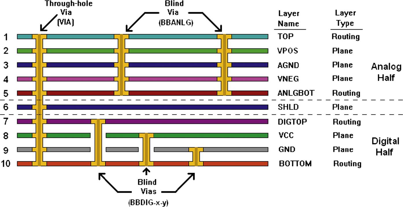
The stack-up in this example demonstrates how to use PCB Editor to implement one method of EMI and cross-talk reduction. A 10-layer board and blind vias are required. The layer stack-up is shown in Fig. 9.120. Since two methods can be used to construct blind/buried vias, both are discussed. The first method is demonstrated on the analog half of the board using a blind via named BBANLG, and the second method (which makes several blind/buried vias simultaneously) is used on the digital side of the board. Since the second method produces multiple vias, the names of the vias have a base name (BBDIG in this example) and a suffix that describes which planes are connected (e.g., BBDIG-x-y). So the middle blind via on the bottom of Fig. 9.120 is BBDIG-VCC-BOTTOM. Both methods are explained in greater detail.
Capture project setup for PSpice simulation and board design
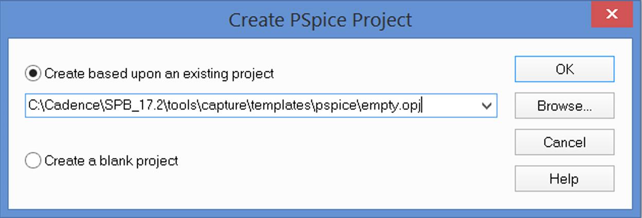
Setting up a Capture project for PCB design and PSpice simulations at the same time has not been widely covered in the literature, so this example addresses that point. Extensive coverage of PSpice simulations in general is not provided in the example, but the process of setting up a project that allows PSpice simulations and the result of a basic simulation are included. To begin a PCB design project that can be simulated with PSpice, start Capture, and from the File menu, select New → Project. When the New Project dialog box is displayed, select the PSpice Analog or Mixed A/D option as shown in Fig. 9.121. Enter a name for the project, use the Browse… button to set up a new folder for the project, and click OK.

When the Create PSpice Project dialog box is displayed, select the Create based upon an existing project radio button and select the empty.opj project template as shown in Fig. 9.122. Click OK. You will need an OrCAD PSpice license to use the PSpice simulator.
Adding schematic pages to the design
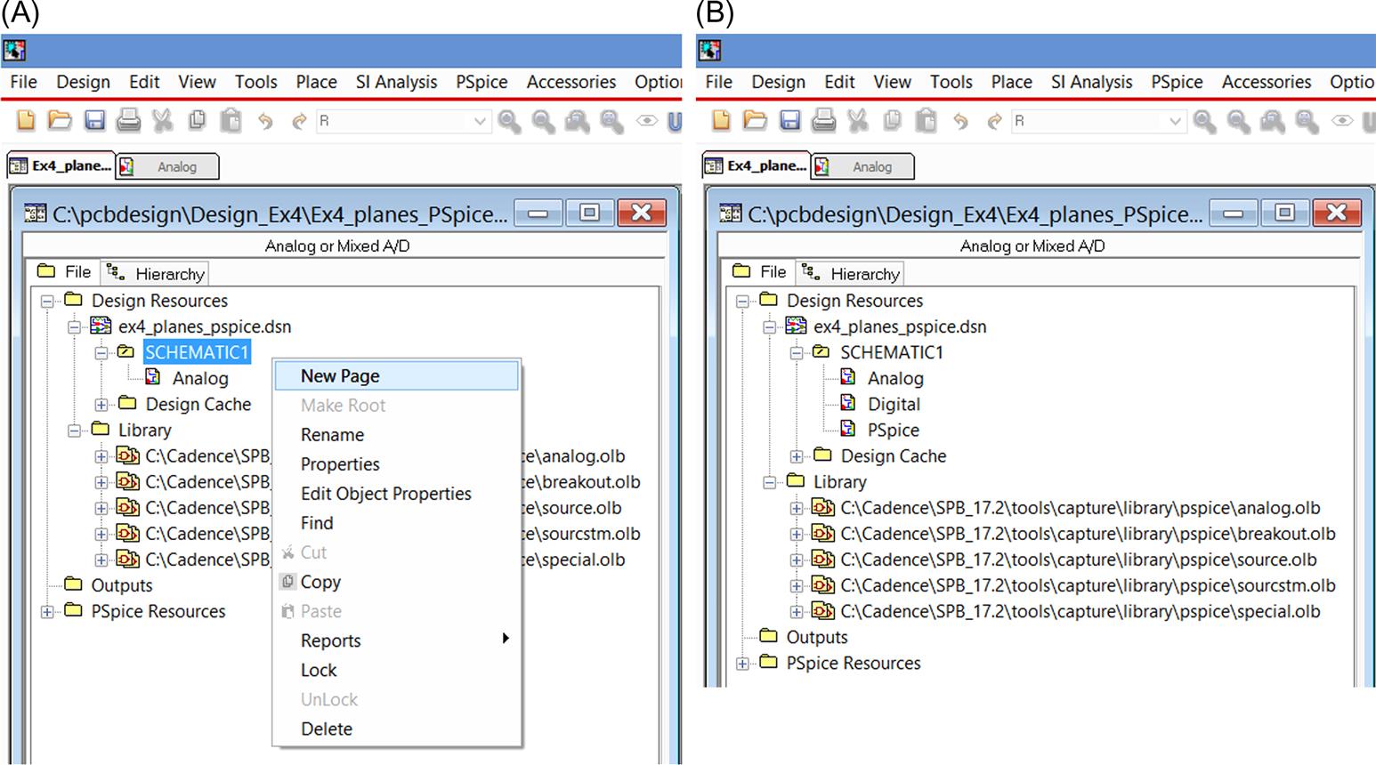
Three schematic pages are needed for this project: one for analog circuitry, one for digital circuitry, and one for PSpice simulation sources. A new project initially contains one schematic page, PAGE1. This page will be renamed, and two more pages will be added. To change the name of an existing schematic page, select the Schematic Page icon, right click, and select Rename from the pop-up menu. Enter the name Analog in the dialog box and click OK. To add a schematic page to a schematic folder, select the SCHEMATIC1 folder, right click, and select New Page from the pop-up menu, see Fig. 9.123A. Enter a name for the schematic (e.g., Digital) and click OK. Add another schematic page to the SCHEMATIC1 folder and name it PSpice. The final schematic page structure is shown in Fig. 9.123B.
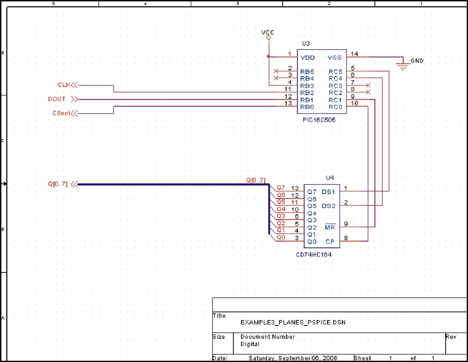
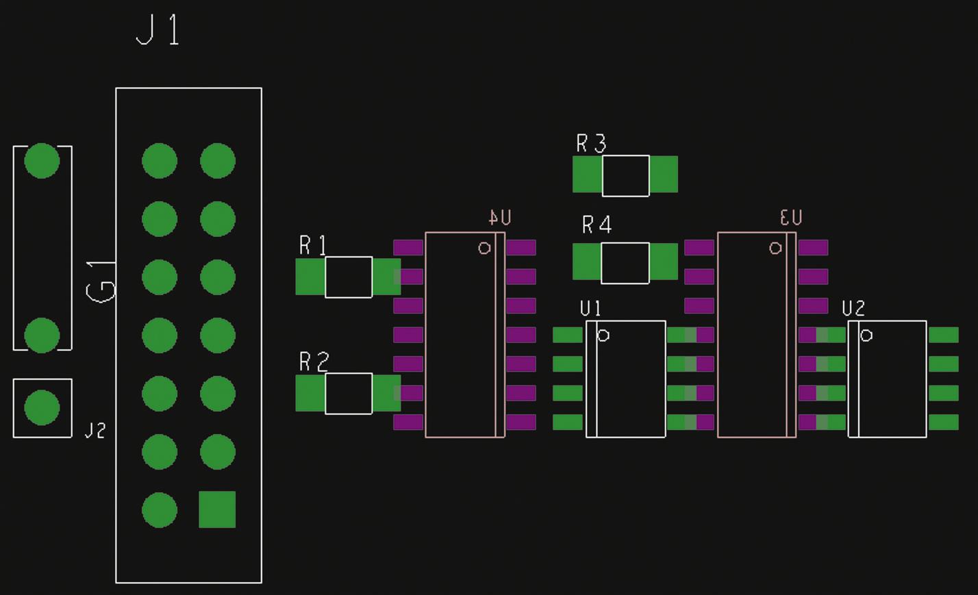
Begin by adding parts to the analog page. To display the analog page, double click the Analog page icon in the Project Manager. The analog page is shown in Fig. 9.124 and includes the passive components (R1-R4), the analog components (U1, U2) and the connector (J1). The U1 part has PSpice model assigned to it which will allow the simulation. The digital components are placed on the digital schematic page (see Fig. 9.127). New items in this project include off-page connectors and multiple ground symbols.

Using off-Page connectors with wires
Generally speaking, off-page connectors are used to continue signal nets across page boundaries. Off-page connectors are used in this example to connect signal lines between the ADC (on the analog page) and the microcontroller (on the digital page) and from the shift register (on the digital page) back to the connector (on the analog page). The off-page connectors are also used here to inject a PSpice signal originating from the PSpice page onto the analog input line (the Sig_Input net is shown in Fig. 9.124 and described later).
To place off-page connectors, select the Place Off-Page Connector tool button,  , on the schematic page toolbar or select Off-Page Connector… from the Place menu. In the Place Off-Page Connector… dialog box, select one of the off-page connector symbols and enter the name to which the connector will be attached in the Name: text box, click OK, and place the off-page connector on the schematic page. You can change the name of an off-page connector after it has been placed on the schematic. To change the name of an off-page connector, double click the name, and enter the new name in the Display Properties dialog box.
Note that the off-page connector to pin 5 on U2 (chip select) does not contain the overbar (e.g., ![]() , indicating an active low line), as does the pin name. Overbars can be generated on Capture schematic parts for nonpower-type pins, but do not use overbars on power symbols, as this will produce invalid netlist names. With PCB Editor, you can use overbars on off-page connectors not used for power nets without producing invalid netlist names. However, overbars on nets do not display the same as pin names. For example, when you make a Capture part, you can put an overbar above CS by typing the pin name as CS, and it will be displayed as
, indicating an active low line), as does the pin name. Overbars can be generated on Capture schematic parts for nonpower-type pins, but do not use overbars on power symbols, as this will produce invalid netlist names. With PCB Editor, you can use overbars on off-page connectors not used for power nets without producing invalid netlist names. However, overbars on nets do not display the same as pin names. For example, when you make a Capture part, you can put an overbar above CS by typing the pin name as CS, and it will be displayed as ![]() . But if you type CS for a net alias name or an off-page connector, it will simply be displayed as CS, which will follow through and be displayed the same way in PCB Editor.
. But if you type CS for a net alias name or an off-page connector, it will simply be displayed as CS, which will follow through and be displayed the same way in PCB Editor.
Off-page connectors cannot be used with power symbols, but they are not required, since power symbols are already global and known by all pages within the design.
Using off-page connectors with buses
Both nets and buses can be connected across page boundaries with off-page connectors. If nets belonging to buses cross page boundaries by off-page connectors, net aliases (using the  button) are not required on the nets because the off-page connectors produce the aliases, otherwise net aliases are required to connect nets to the bus. For example, the nets connected to board connector J1 require aliases to be connected to the bus.
Setting up multiple ground systems on the schematic
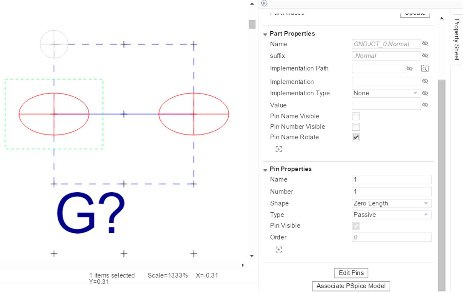
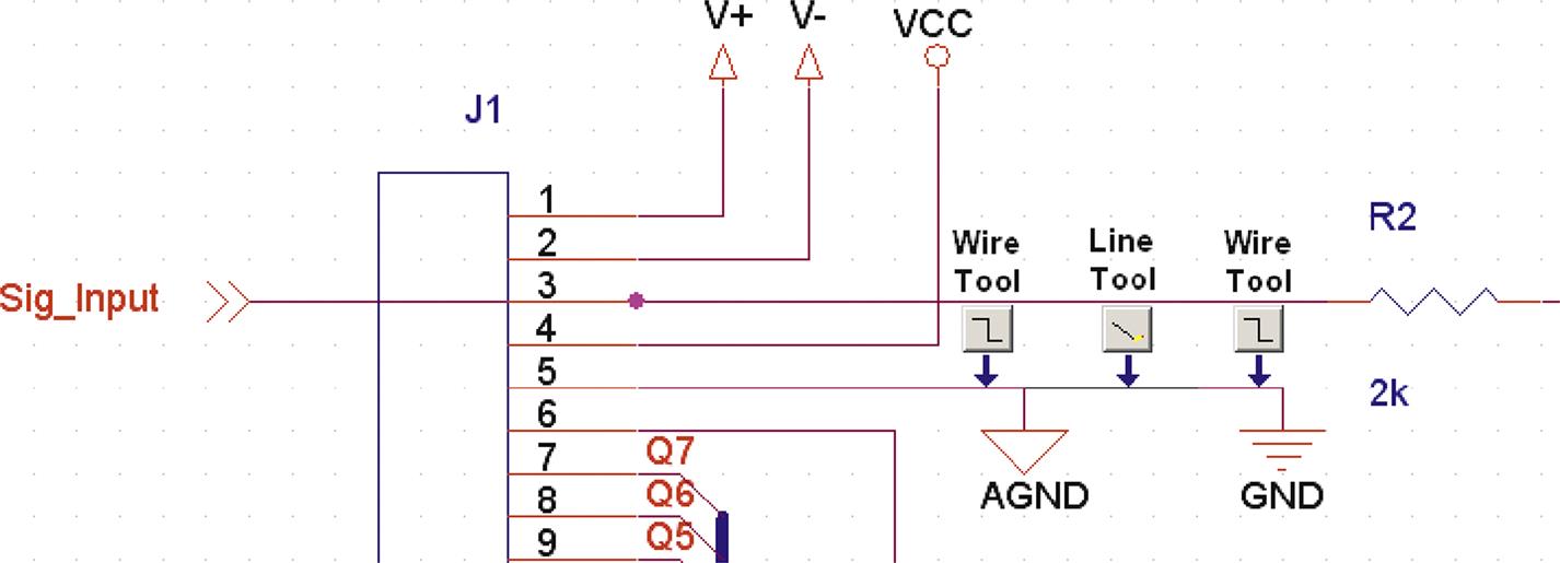
Another difference between this design example and the previous one is the way the ground connections are made. In the previous example, there were two ground symbols (AGND and GND) but only one actual ground net (GND). In that design the grounds were physically separated on the board using a split plane, even though they were still of the same net. In this example, there are three ground symbols and three distinct ground nets (AGND, GND, and SHLD). The shield ground is indicated by a GND_EARTH symbol (renamed to SHLD), it is connected to J1.6 by itself, and it will be the only connection to the plane layer called SHLD. In Fig. 9.124 AGND and GND appear to be jointly connected to J1.5 but are actually separated by the special Capture part symbol G1 (shown in Fig. 9.125 along with the pin properties), which uses the PCB Editor footprint cap300. The footprint can be any two-pin footprint, and cap300 is used for convenience. Capture part G1 is a custom part and is not included with the standard OrCAD libraries but is included as GNDJCT part in the CHAP9EXAMPLES.OLB on the website if you care to see it. Part G1 contains two pins that are graphically connected in the part but are not connected as far as the netlist is concerned. The purpose of G1 is to indicate on the schematic that the grounds are connected, while allowing the grounds to remain separate nets in the netlist.
After the ground connector part has been placed on the board and wired to the appropriate ground nets, you can turn off the part reference (G1) by selecting Do Not Display in the Display Properties dialog box (double click the part reference to show the dialog box).
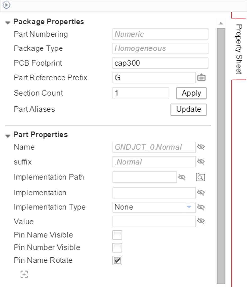
You can also make the pin names invisible to make the part look like a wire. To turn off the pin names, select the part, right click, and select Edit Part from the pop-up menu. In the Part Properties pane (Fig. 9.126), clear the Pin Name (Number) Visible check box.
Note from Fig. 9.124 that a connector, J2, is used with the chassis ground symbol. J2 is a single pin connector with a single padstack footprint that is used to connect the buried shield to the chassis enclosure. When we begin working in PCB Editor, you will see how the three ground connections will be made on the board.
Fig. 9.127 shows the digital schematic page. Off-page connectors are used as described earlier. Unlike on the analog page, where each net in the bus had its own off-page connector, here the bus itself (and all the nets it contains) is attached to a single off-page connector that has the same name as the bus (e.g., Q[0..7]). Note also that off-page connectors are not used with the power and ground symbols, as they are global and known by all schematic pages in the design.
Setting up PSpice sources
Fig. 9.128 shows the PSpice page. Sources are VDC and VSIN, which can be found in the SOURCES.OLB library located in the Cadence Tools/Capture/Library/PSpice folder. Set the VDC and the VSIN source values as shown in the figure.
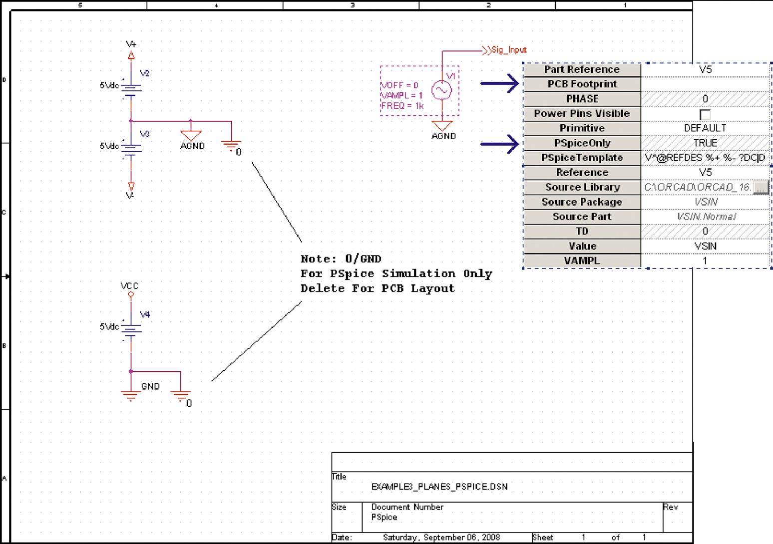
All PSpice simulations require a 0/GND symbol to which all sources can be referenced. The 0/GND symbol is included with the other GND symbols in the CAPSYM library. It is connected to both the analog and the digital grounds only during the simulation. After the circuit has been satisfactorily simulated, the 0/GND symbol must be deleted so that the different ground nets remain separate.
So that no footprints are added for the PSpice parts, make sure all PSpice parts are PSpiceOnly=TRUE and that the PCB Footprint cell is blank. To check these features double click a part to display the Part Properties spreadsheet. A partial spreadsheet is shown in Fig. 9.128.
Any parts that do not have PSpice templates will not be simulated. Parts U3 and U4 and all the connectors have no PSpice templates. When the simulation is run, they will be marked with green dots and ignored.
Performing PSpice simulations
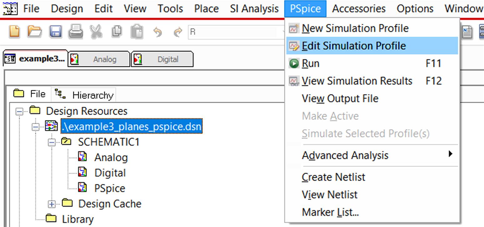
Once the circuit is made, a PSpice simulation profile needs to be established. A default simulation profile is included with the project, because the PSpice Analog or Mixed A/D… radio button was chosen during the project setup. All that needs to be done is to edit it for this design. To edit the PSpice simulation profile, select Edit Simulation Profile from the PSpice menu as shown in Fig. 9.129. If there is no simulation profile in your project, you can create the new one using PSpice → New Simulation Profile.
At the Simulation Settings dialog box (Fig. 9.130), select Time Domain (Transient) from the Analysis type: list. Enter a value in the Run To Time: box to display three or so complete cycles of the waveform (5 ms for a 1 kHz signal). You can specify a value in the Maximum step size: box also, but this is optional. A value that is about 1/1000 of the run time produces very smooth waveforms but takes longer to run. Click OK when you are finished.

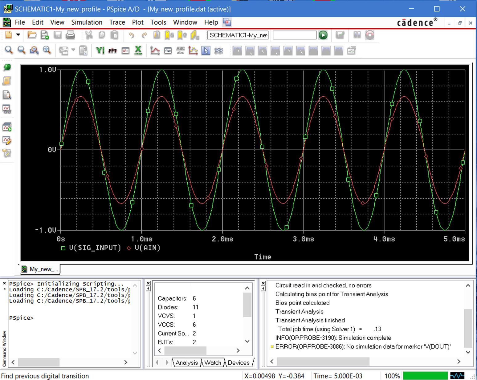
Place the Voltage Markers on the Nets of interest in the Analog schematic page using PSpice → Markers (see Fig. 9.124 as an example with three markers placed). To run the PSpice simulation, click the Run PSpice button (green triangle button) located on the schematic page toolbar (shown in Fig. 9.131).

The PSpice results are shown in Fig. 9.132. Three voltage markers (probes) were placed on the design, but only two waveforms are displayed in the probe window, because not all the parts in the design had PSpice models (PSpice templates) attached to them. PSpice will inform you that not all data were displayed by telling you, No simulation data for marker ‘V(DOUT)’, as is indicated in Fig. 9.132.
To perform time domain simulations, use the VSIN source; to perform frequency domain simulations, use the VAC source and select AC Sweep/Noise in the Simulation Settings dialog box (Fig. 9.130). Many other types of sources can be used to perform simulations. You can even create specialized stimulus files (including noise signals) using one of the VPWL_FILE sources. To see how to use these other sources, see Help → PSpice Documentation or Help → Learning PSpice.
Designing the board with PCB Editor
Once the PSpice simulations are complete and the circuit has been verified, the design is ready to be prepared for PCB Editor. One of the first tasks is to assign (or verify) footprint assignments for all parts. As described in the previous examples, a custom BOM can be generated to list the footprints to make it easier to identify missing or incorrect footprints (see the previous examples and Chapter 10: Artwork development and board fabrication, for details). A sample BOM for this design is shown in Table 9.6. Custom parts and footprints, such as CON1 and CONN14, are available from the website for this book. You can copy them to PCB Editor symbols folder before creating netlist and opening PCB Editor.
Table 9.6

The remaining tasks were described in the preceding text or earlier examples and are listed here without details:
- • Remove 0/GND symbols used for PSpice simulations.
- • Perform an annotation to clean up part numbering (optional).
- • Make sure that global power nets are properly utilized.
- • Perform a DRC in Capture to verify that the circuit design has no issues. Correct any errors and reperform the DRC as needed.
- • Use Capture to generate the netlist and launch PCB Editor.
Create the board outline
As described in earlier examples, set the design size to a size A sheet (Setup → Design Parameters… → Design → Size), and draw a board outline (Outline → Design…).
A 3.00×2.00-in. or larger board is sufficient for this design. Use one of the Place Part tools to place parts inside the board outline. Place digital parts on the bottom side of the board, as shown in Fig. 9.133.
Placing parts on the bottom (back) of a board
To place parts on the bottom side of a board, select the General edit button, select Symbols in the Find filter tab, select the component, right click, and select Mirror from the pop-up menu. Left click off to the side to deselect the part. The part should now be on the bottom of the board. If you do not see the part, make sure the bottom Silk-Screen and associated layers are visible. Check the DRC for footprint and placement problems prior to doing anything else. Use Edit→Mirror to select and mirror several components at once.
Layer stack-up for a multiground system
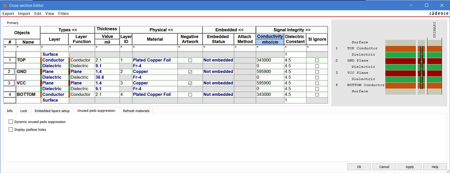
The layer stack-up shown in Fig. 9.120 is used in this design. Set up Power and Ground planes, the Shield plane, and the analog and digital Routing layers as shown in the Cross-section Editor dialog box in Fig. 9.134 (click the Xsection button,  ). To add a layer pair, right click and select Add Layer Pair Above (or Below) from the pop-up menu. Add 16 layers, then name and change the types as shown in the figure (eight Dielectric layers, two Routing layers, and six Plane layers). Select Negative Artwork for all the Plane layers, click the Apply button, then the OK button to complete the setup and dismiss the dialog box. Select distinctive colors to differentiate the planes using the Color tool as described in the earlier examples.

Once the parts are in place and the stack-up is defined, we can pour copper on the Plane layers, perform fan-outs, and begin routing traces on the board. We begin by pouring the copper on the planes.
Adding copper to the planes
As described in the previous examples, use the Plane Outline tool (Outline → Plane… from the menu bar) or one of the Shape Add tools (on the toolbar) to add the copper pours to the Plane layers. Remember that dynamic copper shapes are preferred over filled rectangles or static shapes and to assign each shape to its correct net.
Establishing net, plane, and constraint relationships
The next thing we want to do is to fan out power and ground, but before we can perform fan-outs or route traces, we need to set up blind via definitions and custom routing constraints to limit the layers on which certain nets can be routed. Table 9.7 shows a summary of which layers, vias, and physical constraint sets will be assigned to each type of net. Blind and buried via definitions are described in the next section, and physical constraint definitions are described in the following section.
Table 9.7

Defining blind vias
To use a blind or buried via in a design, an appropriate padstack must exist so that it can be used. If one does not exist, you need to make one. There are two ways to do this, as described next.
Padstacks used as vias exist as library padstacks and board design (layout) padstacks. A library padstack is a padstack definition contained in the symbols library. A layout padstack is a padstack definition associated with a pin or via in a board design. However, when a padstack is used in a board design, its definition (as used) is stored in the board layout file itself and not in any library. So there are two ways to work with via padstacks that are used as blind/buried vias, the first is through the Padstack Editor application and the second is through PCB Editor itself, which is the preferred method in most cases. Only a basic overview of the method using the Padstack Editor is given here. Using Padstack Editor is covered in detail in Chapter 8, Making and editing footprints. Via definitions for this design are made using the second method from within PCB Editor.
Basic overview of using Padstack Editor
To define and store a padstack in the PCB Editor library, you can create one from scratch or you can copy an existing padstack, modify it, then save it with a new name in the library using the Padstack Editor. You can launch it from within PCB Editor or independent of PCB Editor (called stand-alone mode).
To launch Padstack Editor from within PCB Editor select Tools → Padstack and select one of the Modify padstack options.
To make a padstack from scratch using the Padstack Editor in stand-alone mode, go to the Windows Start button on your tool tray and from the All Programs option, select Cadence Release 17.2-2016 → Padstack Editor, as shown in Fig. 9.135.

The Padstack Editor dialog box is shown in Fig. 9.136 opened in stand-alone mode. Using the Padstack Editor, you can construct through padstacks (for through-hole pins on components or for vias), blind/buried padstacks (for vias), or single-layer padstacks (for surface-mount component pins).
Padstack design is covered in detail in Chapter 8, Making and editing footprints, and mentioned only briefly here. In general, you set the drill diameter, pad shapes and sizes. In the Design Layers tab, you can specify layers in addition to the default ones. By selecting specific layers and certain types of connections, you can use this tool to construct blind/buried vias.
You can also launch the Padstack Editor from PCB Editor by selecting Tools → Padstack → Modify Padstack from the menu. You can modify library padstacks or padstacks associated with the design only.
To use the Padstack Editor, you need to duplicate the layer stack-up in your board design and specify a specific layer/pad combination that satisfies the via requirements. The via padstack is saved to the library or the design and assigned to specific nets in the board design. This approach can be cumbersome, and the via is easily reusable in future designs only if they have an identical layer stack-up.
The other method is to set up vias interactively from the design using the BBvia tool. This is the easiest way to make a blind or buried via, because all the layer definitions are known, and set up, by the BBvia tool. Interactive design of blind and buried vias is initiated by selecting Setup → Define B/B Vias, as shown in Fig. 9.137, where you can select from two different methods of interactively designing custom blind and buried vias.

If you select Define B/B Vias…, you get the dialog box shown in Fig. 9.138. This method is used for the analog half of the board (see also Table 9.7). Give the via a name (BBANLG in this example, for blind/buried analog) and select a padstack to copy from. This sets the basic definition of the new padstack (e.g., drill diameter and pad shapes and sizes). The Start and End layer entries define how “tall” the padstack will be (see Fig. 9.120). So in this example, if you choose VIA as the padstack to copy (which of course is a through-hole padstack), the new padstack will be identical to it but will not go all the way through the board (it will go between only the Start and End layers). This method creates one padstack that goes from the Start Layer to the End Layer and includes all the layers between them. Click OK when finished or AddBBVia to make another one.

If you select Auto Define B/B vias…, then you get the dialog box shown in Fig. 9.139. We use this method to make the blind vias for the digital half of the board. Again select a padstack on which to base the new one. Check the Add prefix box and select a prefix name. Select the Start and End layers as before. You can select which layers will be used in setting up the via; we use all the layers in this example. Once the settings are entered, click Generate to start the process. Click Close when finished.

This method actually makes several vias. Essentially, it makes as many blind and buried vias as necessary to connect each of the adjacent planes (two layers at a time) and to connect the Start and End layers to each other and to each of the internal layers. You can view the bbvia.log file, and in this example, the following padstack vias were created:
So any via that has BOTTOM in its name is a blind via, and the others where BOTTOM is not included are actually buried vias. One of the vias will never be used in this example, VCC-GND, because it would short the Power plane to GND and result in a scrapped board. Once the planes and vias are defined, we will assign the proper via(s) to each of the nets.
Assigning vias to nets
Use the Constraint Manager to assign vias to the nets. Open Constraint Manager by clicking the Cmgr button,  , on the toolbar. Select the Physical tab, and select All Layers under the Net folder. In the Vias column, you will see a listing of all vias in the design (including the default, Via). Select a net to modify by selecting the cell in the Vias column for that net. The Edit via list dialog box will be displayed, as shown in Fig. 9.140.
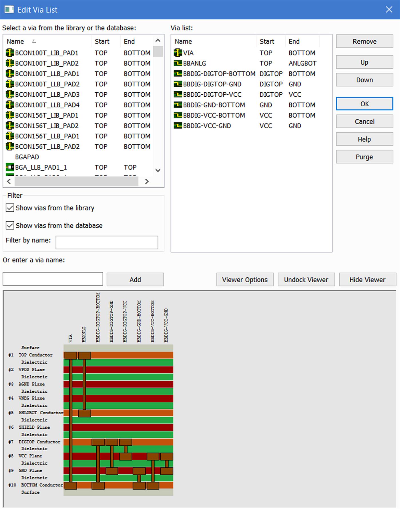
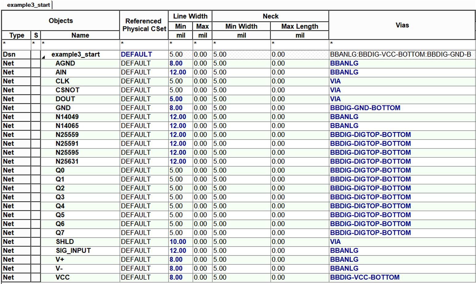
Note that the BBANLG is in the “available” list but not in the “used” list. Add the BBANLG via to all of the analog-related nets (including V+, V-, and AGND). Remove any vias that are prohibited or unnecessary. The final setup is shown in Fig. 9.141. Notice that the CLK, CSNOT, and DOUT nets use the default via, VIA, since it is a through-hole padstack, and these nets need to pass through the Shield layer (to connect the ADC on the analog side to the microcontroller on the digital side). Although the SHLD net does not need a via, the default via, VIA, is assigned to it because each net must have at least one via assigned to it, so the default via was assigned. Next we see how to restrict the routing of certain nets to specific layers.
Assigning nets to layers using custom, physical constraints
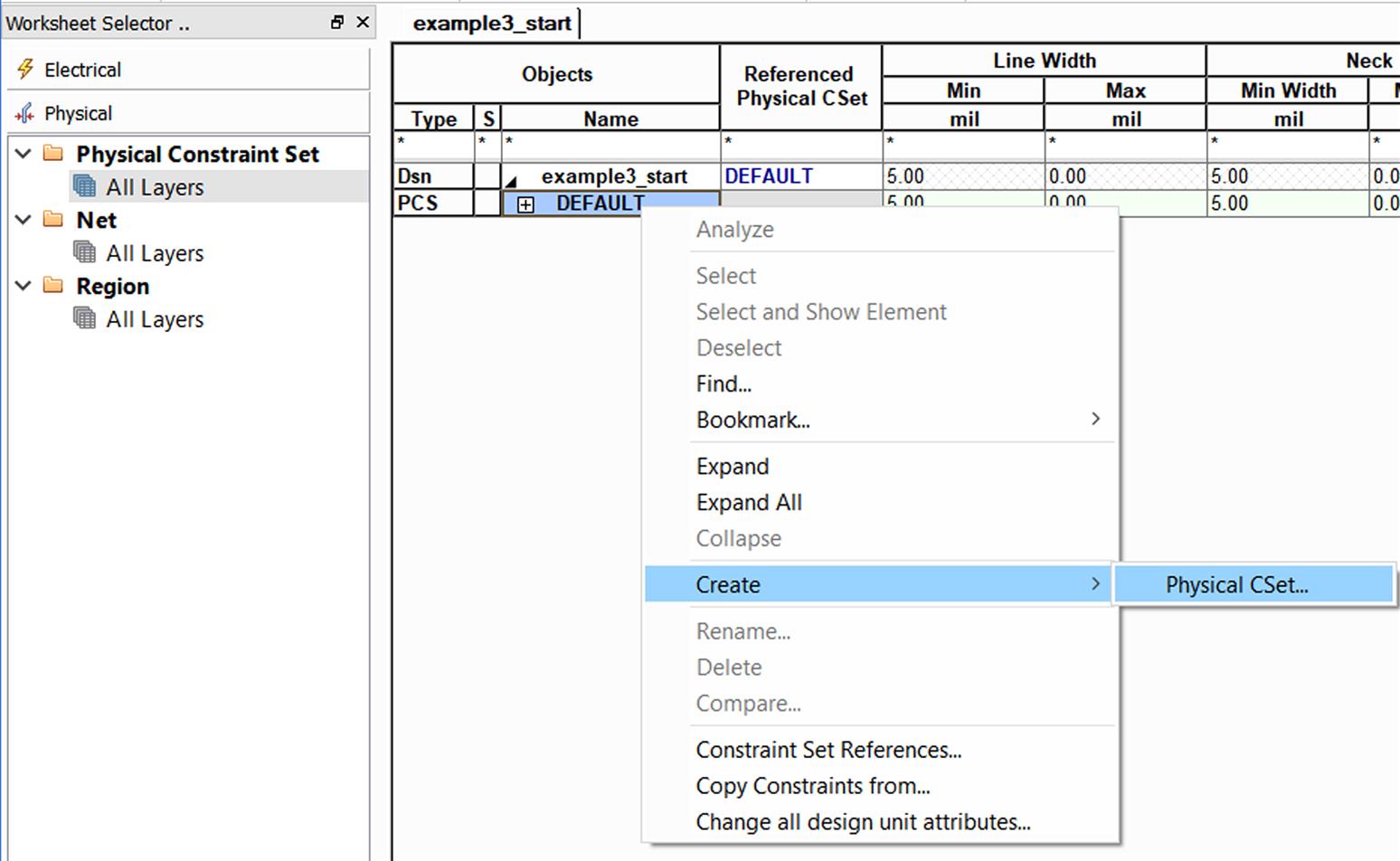
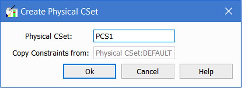
The next step is to assign nets to the proper Routing and Plane layers. The net layer assignments are shown in Table 9.7. To make net layer assignments, we need to set up new physical constraint set (CSet)—the custom set of rules which we can use later for some of our nets. To create the new Physical CSet, left click on the All Layers icon in the Physical Constraint Set folder of Constraint Manager, and select Create → Physical Cset from Objects menu (Figs. 9.142 and 9.143). Set the new name of your custom CSet and press OK. You will see the new row in the list of CSets, below the DEFAULT constraint set.
In this example, we use the constraint set to limit routing to specific layers, so the appropriate flag is set to FALSE under the Allow Etch column in the certain layers, as shown in Fig. 9.144.

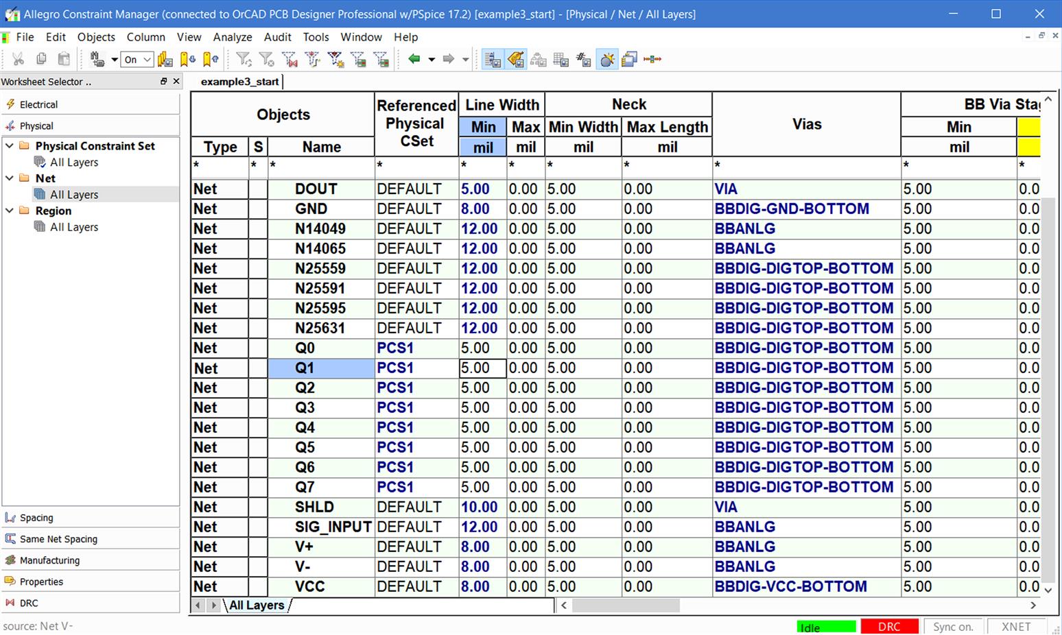
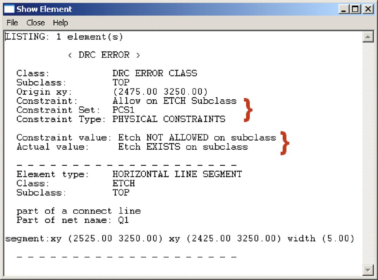
Once the constraint set is defined, assign it to proper nets (see Table 9.7). To assign a constraint set to a net, select the All Layers icon under the Net folder (see Fig. 9.145). Select (using left mouse button) the cell or cells in the Referenced Physical CSet column for the nets to which you want to assign the new constraint. When you select the cell(s), a dropdown list will be displayed. Select the desired constraint set from the dropdown list. As shown in the figure, the new constraint, PCS1, was selected for the digital bus traces. With this constraint the autorouter will route these traces only on the DIGTOP and BOTTOM layers. If these nets are routed manually on a layer not included in the constraint set, DRC errors will be issued (see Fig. 9.146 as an example).
Continue naming and assigning constraint sets to the nets as outlined in Table 9.7.
Once vias have been assigned to nets and nets have been assigned to layers, the next step is to begin the fan-out process.
Fan-outs using blind vias
Once the vias are set up and assigned to the nets, we can begin performing the fan-outs. We do the first couple of ones by hand so that you can see how it works. We begin by doing the first fan-out for VCC. Make all the Plane layers and nets invisible except VCC. Set the Etch grid to 25 mil (All). Zoom to the area around U3 (PIC16C505) and locate pin U3.1 (check the Pins option in the Find tab if necessary). Select Add Connect… and click on the pin (make sure Pins is checked in Find tab). Route a small section out from the pad and left click to place a vertex. Display the Options tab (see Fig. 9.147) to make sure that the two layers involved are Bottom and Vcc and that the BBDIG-VCC-BOTTOM via is available. Then right click and select Add via from the pop-up menu. A bbvia should be inserted. Right click and select Done. Note that the correct Alt layer has to be displayed in the Options tab or you may not be able to place a via if the via assigned in the Constraint Manager cannot physically make a connection from the Act. (active) layer to the Alt. (alternate) layer displayed in the Options tab.

If you toggle back and forth between the Bottom, Vcc, and GND layers, you should see that the via connects the trace and pad on the bottom to the VCC plane, and a clearance area around the via is on the GND layer. If you toggle through the analog planes, you should see no evidence of the trace or via at all.
Next we try one of the analog fan-outs. Locate resistor R3 and its pin R3.2. We will route a fan-out from this pin to the analog Ground plane. In the Constraint Manager, make sure that the AGND net (and layer) is visible and able to be routed. If you don't see AGND or GND net in a list, check if you removed the connections of AGND and GND to PSpice 0 net in the third page of schematic design which was made for simulation purpose. Select the Add Connect… tool, click on the R3 pad to start a trace, and left click a short distance (about 50 mil) to place a vertex. Check the Options tab and make sure that the active layer is Top, and the alternate layer is AGND, and that the BBANLG via is available. Right click in the work space and select Add Via from the pop-up menu.
Note that the process of using the blind via fan-outs is the same no matter which method was used to generate them. Now we use the autorouter to place the rest of the fan-outs.
We fan out the remaining AGND and Vcc nets and complete all the V-, V+, and GND fan-outs using the autorouter. Open the Constraint Manager, and make sure that all the power, and ground nets are visible, and no routing restrictions have been placed on them. Select Route → PCB Router → Route Automatic… from the menu. As described in detail in the previous examples, use the Automatic router dialog box to set the fan-out parameters. As a summary select the Router Setup tab, and in the Strategy group box, select the Specify routing passes radio button. Select the Routing Passes tab, and select only the Fanout option in the Pass Type column. Click the Params… button to display the router parameters dialog box. Select the desired options, such as Power Nets, and click OK to dismiss the dialog box. Click the Route button to perform the fan-out. You can also use the Create fanout tool to fan out pins and components.
An example of a completed fan-out is shown in Fig. 9.148. Notice where a via goes from Bottom to GND (digital GND) on U3 right under the corner of the pad on R4. Note also that this does not cause a DRC error, because the via under the pad of R4 does not go all the way through the board and therefore does not touch R4. Other occurrences of this type are shown on the pads for the ICs.
Once all the fan-outs are complete, the rest of the board can be routed. Set up the autorouter as described in the previous examples, and route the rest of the board. As a quick overview, select Route → PCB Router → Route Automatic… from the menu. At the Automatic router dialog box, select the Router Setup tab, and in the Strategy group box, select the Specify routing passes radio button. Select the Routing Passes tab, uncheck the Fanout option in the Pass Type column, and select the Route and Clean options. Click Params... and check the Signal Nets checkbox.
Click OK to dismiss the dialog box. Click the Route button to route the board.
Note: Designs like this can be tricky. If the autorouter has difficulty routing the board or performing the fan-outs, make sure that all the Plane layers and design constraints are set up properly, the proper vias are assigned to the correct nets, and the appropriate nets are enabled.
An example of the fully routed board is shown in Fig. 9.149. The grid and all the Plane layers are turned off so that it is easier to see the traces.
Alternate methods of connecting separate Ground planes
In this example the two Ground planes are electrically separate and the component G1 in the schematic is used to connect the planes on the board by soldering a wire jumper, an inductor, or ferrite bead in the G1 footprint. In the following sections, alternatives to inserting and soldering the wires or components are discussed. The first alternative is to short the G1 padstacks with copper, and the second alternative is to short the planes with a shorting padstack.
Shorting the planes with copper etch
To reduce assembly complexity, a copper etch object can be used to short G1’s padstacks rather than soldering a wire or installing a component into the footprint. The copper etch can be a trace or a copper area. To add a thick trace across the padstacks, select the Etch/Top classes in the Options pane. Select the Add Line tool, and from the Options pane, set the line width to 30 mil or so. Left click on the first padstack of G1 and draw a line (trace) to the second padstack. The copper etch line is shown in Fig. 9.150A.

Another way to make the connection is to use a copper area. To do so, select the Shape Add Rect tool. In the Options pane, select Static solid as the Shape Fill Type. You can leave the Dummy Net assigned to the shape. The static solid is shown in Fig. 9.150B.
When using either of these etch objects, DRC errors will occur because the shapes violate pad spacing rules. Since this is what we want, we can override the DRC errors. To do so, click the Waive DRC button on the toolbar or select Check → Waive DRCs → Waive from the menu. Make sure that the DRC Errors option is checked in the Find filter pane, then left click on the DRC markers to override them. Another way to avoid the DRC errors is to attach the NET_SHORT property to this shape. Select the shape, and right click, then choose Net Short from the pop-up menu, and then left click over each net to be connected together. Right click and choose Complete Net Short.
Shorting the planes with a Padstack
Rather than take up space on the board using a dedicated footprint, you can use a via attached to one of the Ground planes and modify it so that it is attached to both Ground planes at the same time. We place a VIA on the board, attach it to the GND plane, and modify it so that it is connected to the AGND plane too.
When using this approach, the special part (G1) in Capture is not used. Instead a small segment of a graphical line—using the Place Line tool instead of the Place Wire tool—is used to indicate that the two grounds are connected at the header pin. This eliminates the footprint in PCB Editor.
Go back the schematic page, and delete part G1 in Capture. Use the Place Line tool to make the AGND and GND nets look like they are connected as shown in Fig. 9.151. The Line tool is graphical only and does not create a connection in the netlist.
Perform an ECO to forward annotate the changes to PCB Editor as described in the earlier examples. In short, save the board design, and close PCB Editor. In Capture select the project icon, select Tools → Create netlist… from the menu. Select the PCB Editor tab, check the Create or Update PCB Editor Board box, and relaunch PCB Editor. When the board design is reopened, the footprint for G1 should be gone.
The next step is to place a generic via on one of the planes and modify the via to connect it to the other plane. To do so, you should add VIA to the list of available vias for GND net in Constraint Manager. Then select the Add Connect tool, and from the Options pane, make the GND plane (class) as the active class and the Top layer as the alternate. Select Shapes in the Find pane. Left click on the GND plane near the connector J1 to place a vertex and start a trace. Immediately right click and select Add Via from the pop-up menu; right click again and select Done from the pop-up menu. The via (which should be padstack VIA) is now connected to the GND plane but nothing else.
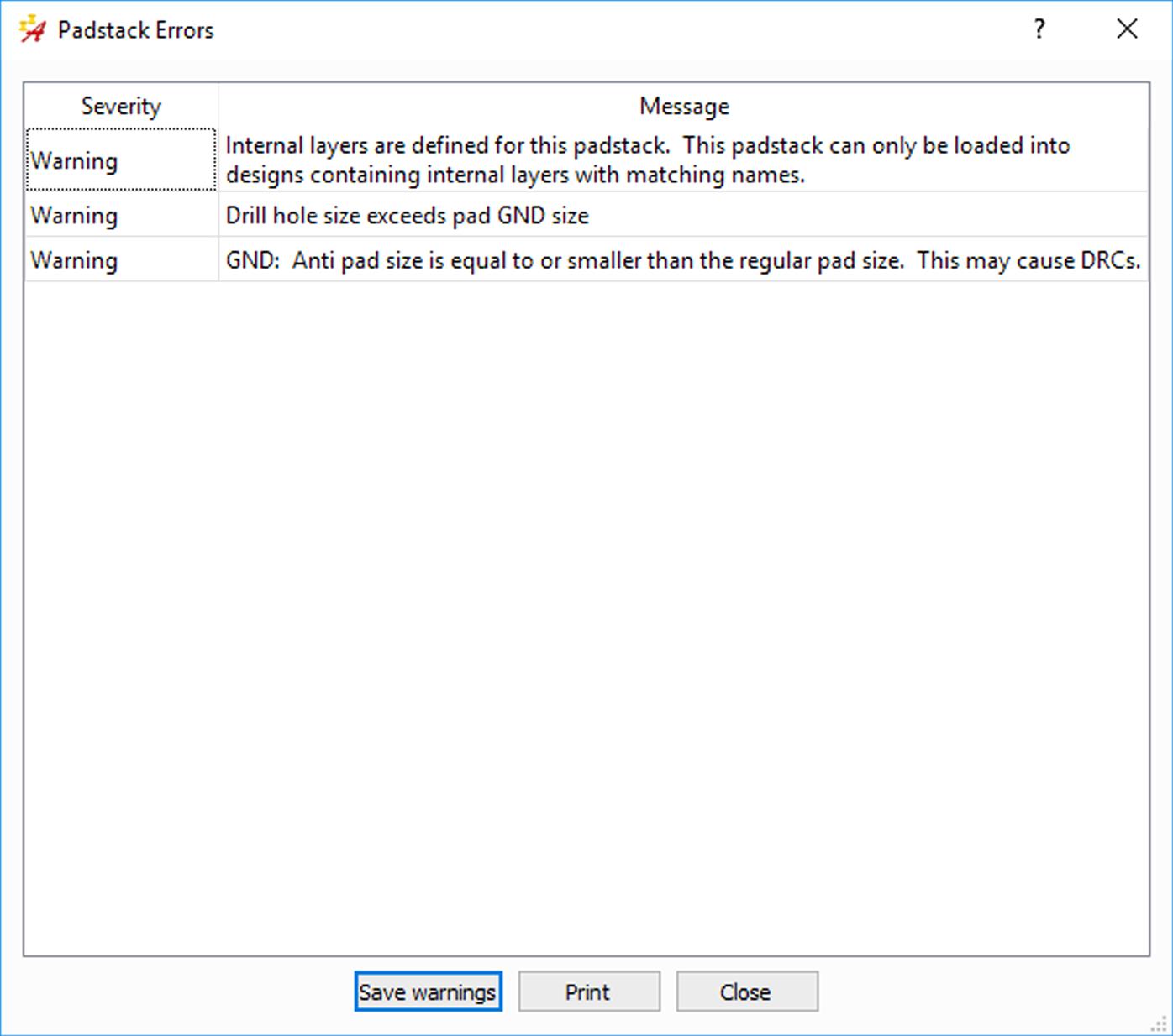
To modify the via, select Tools → Padstack → Modify Design Padstack… from the menu. Left click the via in the canvas to select it. In the Options pane, select the Instance radio button (see Fig. 9.152). The original VIA name will be listed, and a new via VIA-1 will also be listed. Click the Edit… button to display Padstack Editor. The Padstack Editor, Design Layers tab, is shown in Fig. 9.153 with the new padstack settings. Note that the Anti Pads are set to 5 mil in those layers we want to connect, which is much smaller than the drill diameter. So, when the holes are drilled into the board during the manufacturing process, the small clearances will be drilled away, and the copper on the planes will butt up against the drill hole. Then, when the hole is plated, the plating will short the planes together. Remember to add clearances to the other plane layers (e.g., Vcc and SHLD), or they will be shorted to the planes too.


To save the changes, select File → Update to Design and Exit… from the menu. A warning box will be displayed telling you that the Anti Pad will be drilled away (see Fig. 9.154). That is what we are after, so close the warning box. Another warning will be displayed (see Fig. 9.155). Click Yes to complete saving the changes and quit editing.

To allow via to connect two nets together without creating DRC marker, switch to General Edit mode, check only Vias in the Find pane, select the via, right click and choose Net Short. Then left click over each net to be connected together. Right click and choose Complete Net Short.
Note: This method is not necessarily recommended, since connection between the two Ground planes is not automatically “documented” by the software. The process should be manually documented on the schematic, and some type of marker should be placed in silk screen on the board, indicating which via is shorting the two planes together. In the event that some problem occurs and the planes need to be separated, it would be a simple matter to drill out the via. If the via is not marked somehow, it would be impossible for someone not familiar with the board design to know where or how the planes were shorted together. Even if a person were to look at the design in PCB Editor without some markings in the design, the only way to tell which via is shorting the planes is to look at all of the padstack definitions or create a Waived Design Rules Check Report (if the person happened to think of it) or look for NET_SHORT properties.
This concludes the third design example.
Example 4. High-speed digital design
This example demonstrates how to stack-up layers and design transmission lines for a high-speed digital PCB. The example also demonstrates how to create a moated ground area with a bridge around a high-frequency crystal oscillator, how to perform pin/gate swapping, and how to create a heat spreader using vias to the Ground plane. The example circuit is shown in Fig. 9.156.
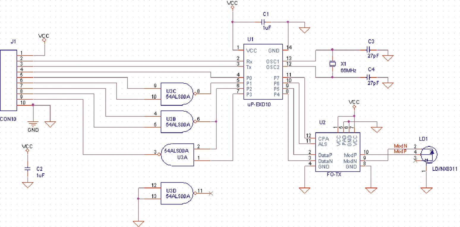
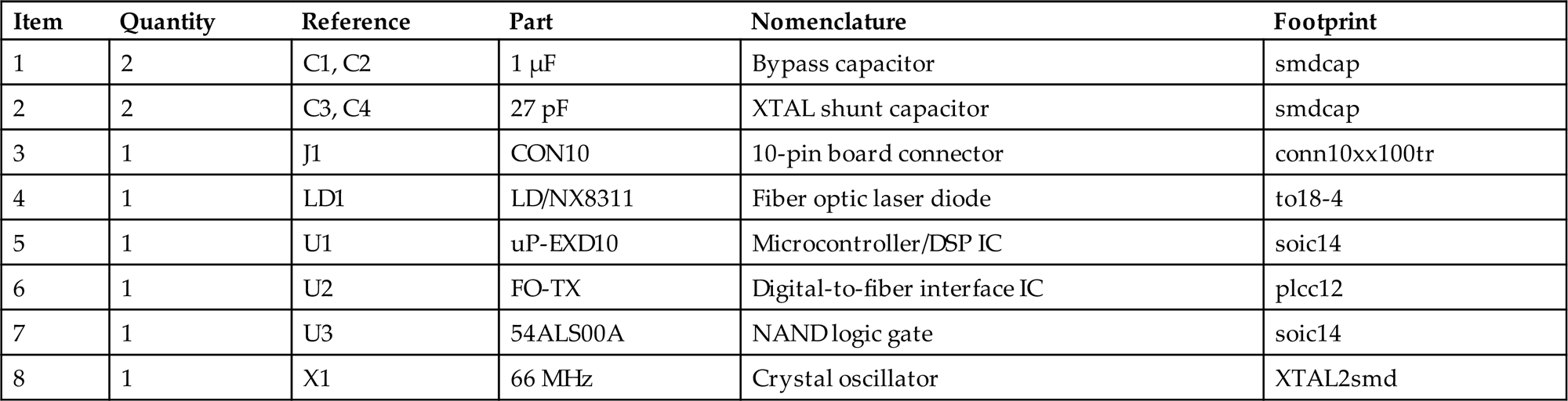
The BOM for this example is shown in Table 9.8. The circuit consists of a (fictional) high-speed, low-pin-count microcontroller/digital-signal processor (uP-EXD10) driven by a 66-MHz clock (X1), a digital-to-fiber optic interface IC (FO-TX, which mimics an ADN2530 but with fewer pins), a fiber-optic laser diode (LD1), and a couple of 54ALS00 NAND gates used for I/O decoding. The digital signals have rise and fall times from 200 ps to 1.9 ns and require controlled-impedance traces (see the Analog Devices ADN2530 data sheet for an example application). In a real design, more bypass capacitors would be used on the circuit, but the design is scaled down to keep the design simple. The parts and footprints are located on the website for this book.
Table 9.8
Using the procedures described in the earlier examples, start a new Capture project, and place and connect the parts as shown in Fig. 9.156. After completing the schematic, make sure all footprints are assigned to the parts and create the netlist for and launch PCB Editor.
Start a new board project using the procedures described in the previous examples.
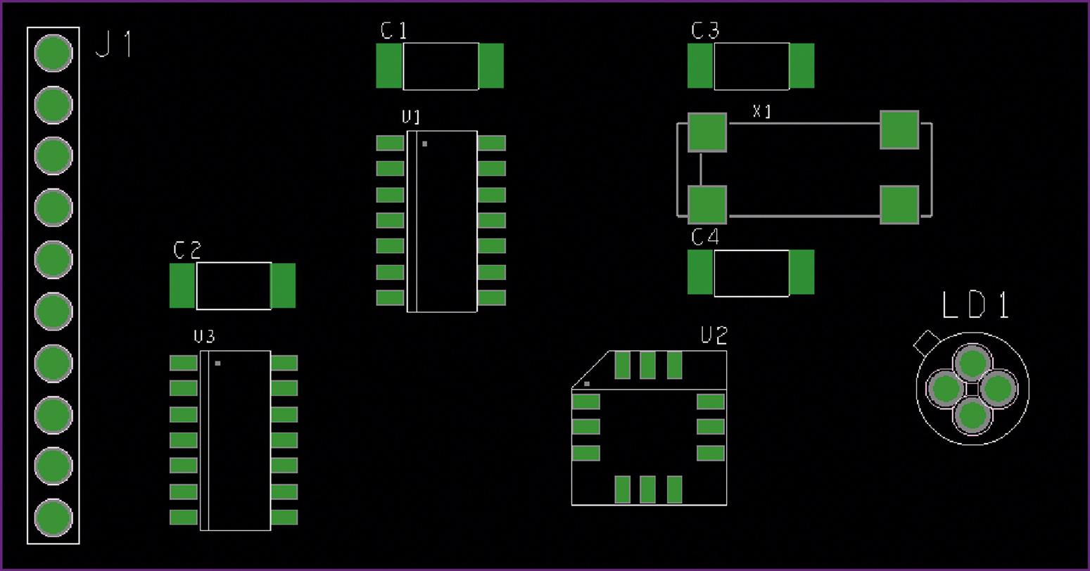
As in the previous examples, the first step is to make a board outline and place the parts inside the boundary. The initial board layout is shown in Fig. 9.157. Signal flow is from left to right, with the highest frequency components located close together near the laser diode connector on the right side of the board.
The next few steps were covered in detail in the previous examples. The following tables and figures show the design parameters for this example, but step-by-step instructions are not repeated here. The required steps are to (1) define the layer stack-up and enable the appropriate layers using the Cross Section Editor dialog box, (2) define two vias in addition to the default VIA using the Padstack Editor and Constraint Manager, and (3) fan out power and ground for the surface-mounted components.
Layer setup for microstrip transmission lines
Since there are so few parts, a simple four-layer board design is used. The layer stack-up and net assignments are shown in Fig. 9.158. The layer thicknesses depend on the board manufacturer; the values (units in mil) shown in the figure are typical. The Top layer and Ground plane will be used to route surface-type microstrip transmission lines and most of the lower-speed digital traces. Only low-speed traces that cannot be routed on the top will be routed on the bottom layer.
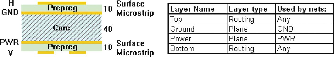
Fig. 9.159 shows the layer stack-up as defined in the Cross Section Editor dialog box. Notice that the material thicknesses have been added.
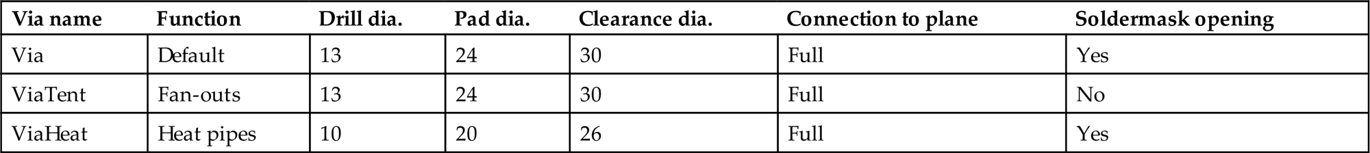
Three via types are used in this example (see Table 9.9). VIA is the default via included in the symbols library folder, while VIATENT and VIAHEAT are custom vias (included in the design folder on the book’s website). VIATENT is similar to the default VIA but is tented (i.e., the padstack contains no soldermask opening definitions) and used here for the fan-outs as a demonstration. Multiple copies of VIAHEAT will be used as heat pipes to connect a thermal pad (a copper pour area) beneath U2 to the Ground plane and function as a heat spreader. VIAHEAT has smaller dimensions so that they can be placed close together to provide low resistance to heat flow to the ground plane.
Constructing a heat spreader with copper pours and vias
The design of heat spreaders on PCBs depends significantly on the type of device and how it is attached to the board. For design examples and thermal management calculation, see the application note references listed in Appendix E. The heat spreader demonstrated here is based on design suggestions described in the ADN2530 data sheet.
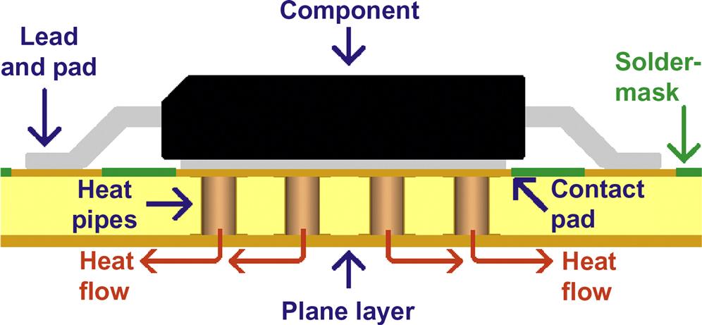
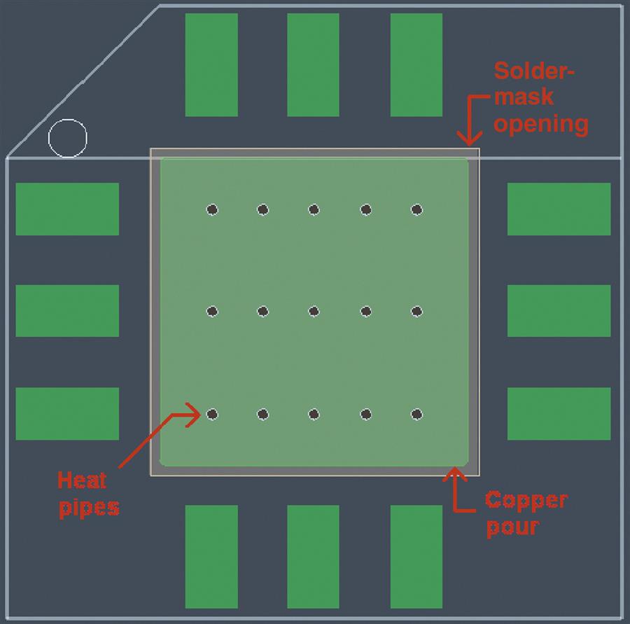
Before the board is fanned out or any traces are routed, the heat spreader is put into place so that the router avoids that area, thereby preventing having to rip up and reroute fan-outs or traces. A functional diagram of one type of heat spreader is shown in Fig. 9.160. The silicon die inside the component is thermally bonded to a metal pad on the bottom of a specially designed package. The pad is in turn thermally bonded (either by soldering or thermal compound) to a copper area on the top layer of the PCB. The copper area has an opening in the soldermask and multiple vias to connect it to a Plane layer (either ground or power depending on the chip design). The vias function as thermal conductors (heat pipes) that allow heat to flow away from the component. If a component dissipates excessive heat, the Plane layer can be mechanically (and thermally) connected to a larger heat sink or other mounting hardware to help dissipate the heat.
Via design for heat spreaders
Before we begin to construct the heat spreader, we need to define the VIAHEAT padstack. To make the heat pipe efficient at conducting heat, solid connections to the plane are used rather than thermal reliefs. To define the new via (VIAHEAT.pad), we begin with an existing padstack, save it with a new name, modify it to our specifications, then save it. If you have your board design open, launch the Padstack Editor by selecting Tools → Padstack → Modify Design Padstack… from the menu bar. Display the Options tab, select Via from the list, then click the Edit… button.
Before making any changes to the padstack choose File → Save as… from the menu bar. An information window will be displayed with the following warnings:
Drill hole size exceeds pad size.
Click the Close button to dismiss the window (this will be explained shortly). When asked Save with warnings? click Yes. Save the padstack as VIAHEAT.pad in either the working directory or the symbols library.
Using the Parameters and Layers tabs as shown in Fig. 9.161 modify the padstack per the specifications in Table 9.9.
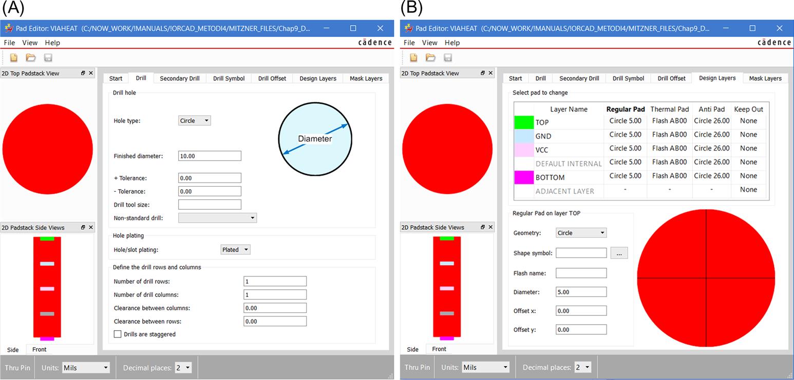
Since the top and bottom pads in this padstack are smaller than the drill diameter, they will be drilled out. Normally, we would not want this, but in this example, many vias will be placed side by side, and a copper rectangle will be placed over the whole group and will act as one big pad for the entire group of vias. Top and bottom pads can be left in place, but it is visually more appealing in the design if the pads are not shown.
Note also that the soldermask is left rather large but could have been removed because, as will be shown later, one large soldermask opening will be placed on the board to expose the heat spreader and heat pipes and will overwrite the individual soldermask openings.
After the VIAHEAT padstack is finished and saved, repeat the process to create the tented via, VIATENT, which will be used as the default fan-out via. The VIATENT padstack is identical to the default VIA padstack, except that no soldermask openings are defined, as shown in Fig. 9.162.
Once the VIAHEAT padstack is finished, use the Constraint Manager to assign it to the GND net, as shown in Fig. 9.163. To assign a via to a net, left click in the cell to display the Edit Via List dialog box, as shown in Fig. 9.164. Left click a via twice in the left-hand box to add it to the Via list box.

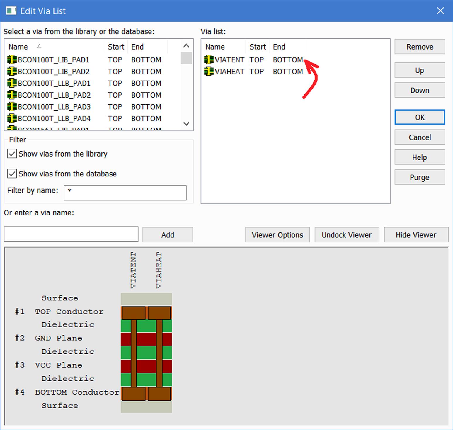
You can also remove vias from the Via list by left clicking the one you want to remove, then clicking the Remove button. The via at the top of the list will be the default via. To change the priority of use, select the desired via and click the Up or Down button to move the via within the list. When you are finished, click OK. The ground layer will need the VIATENT via for the fan-outs and the VIAHEAT via for the heat spreader, so assign both vias to the GND net. All other nets get only the VIATENT via, and no nets should be allowed to use the VIA via (select VIA and click the Remove button).
Now that the heat pipes have been defined, we can build the heat spreader. We begin by placing a copper plate on the Top layer to define the boundaries of the heat spreader. To do this click the Shape Add Rect button on the toolbar, display the Options pane, and select the options shown in Fig. 9.165.

Draw a copper pad in the center of the footprint, as shown in Fig. 9.166. Note: You may need to adjust the grid settings (Setup → Grids) to achieve the necessary drawing resolution.

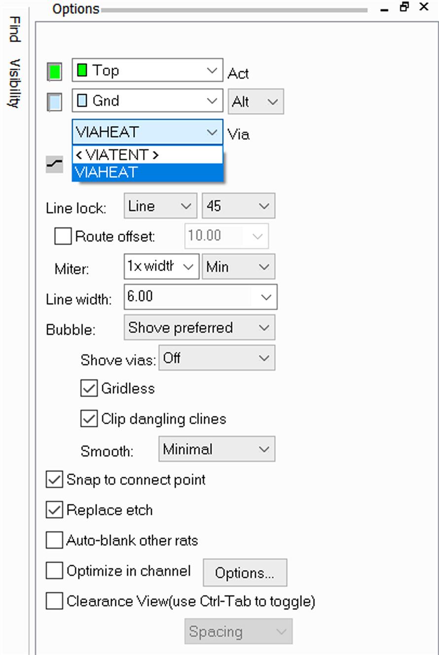
The next step is to place the heat pipes. To do this, begin by clicking the Add Connect button. Display the Options pane, and select GND as the active layer (Act) and Top as the alternate layer (Alt). Left click on the design at the insertion point. Display the Options pane again, and select VIAHEAT from the via list (see Fig. 9.167). Move your mouse back over to the design area, right click and select Add via from the pop-up menu. A VIAHEAT via should be placed. Repeat this process for each pipe. See Fig. 9.168 for reference.
Note that you can easily place many vias at once using the via array generator. As an alternative to placing the heat pipes in the board design, you can make a custom package that includes the heat pipes and copper plate.
For a good thermal connection to occur between the package and the heat spreader, an opening needs to be made in the soldermask. To make an opening in the soldermask, select the Shape Add Rect button on the toolbar, then select the Package Geometry class and Soldermask_Top subclass from the Options pane. Draw a filled rectangle over the copper pad that is 5 mil larger than the pad on all sides. If the thermal bond will be made by SMT soldering, repeat the preceding steps to place a filled rectangle on the Package Geometry class and Pastemask_Top subclass.
Note: Many of the footprints included in the library do not have a pastemask defined in the Package Geometry class. So, if you are planning to use pick and place assembly, you must modify some of the footprints to include the pastemask definitions.
The finished heat spreader is shown in Fig. 9.168. At this point click the Fix button (the green thumb tack), and fix all the vias and the dynamic copper plate so that they are not removed by the autorouter or any routing or cleanup processes.
The next step is to fan out the board. Earlier, we used the Constraint Manager to establish net default vias, but when the autorouter is used to fan out a board, it uses the design default vias. To change the default design via, open the Constraint Manager, select the Physical tab and the All Layers icon under the Physical Constraint Set folder. Select the DEFAULT constraint set. Left click the cell in the Vias column. In the Edit Via List dialog box, select the VIATENT via to add it to the list, and remove the VIA via, and click OK.
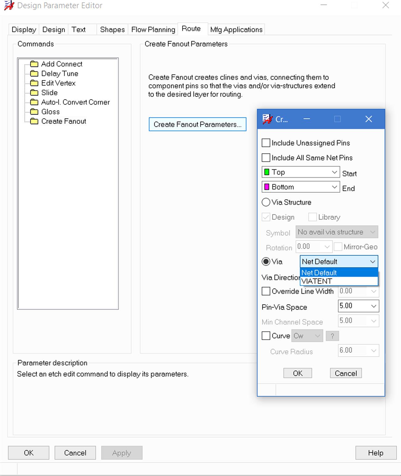
Now you can set the fan-out parameters using VIATENT. To set fan-out parameters, select Setup → Design Parameters from the menu bar. In the Design Parameter Editor, select the Route tab, then click the Create Fanout Parameters button, as shown in Fig. 9.169. In the Create Fanout Parameters dialog box, you can now select VIATENT whereas it would normally list only VIA.
Once these settings are correct, perform the fan-out as described in detail in the previous examples. In summary, select Route → PCB Router → Route Automatic… from the menu bar. At the Automatic Router dialog box, select the Router Setup tab, and select the Specify routing passes radio button. Next, select the Routing Passes tab, select the Fanout and deselect the Route and Clean options, click the Params… button. In the SPECCTRA Automatic Router Parameters dialog box, select the Fanout tab. In the Pin Types section, select the Specified: button, select the Power Nets, and deselect all others. Click OK, then click the Route button.
Once the router has finished, it is a good idea to check the vias to make sure PCB Editor did what you asked and performed the fan-out using the right via. To check the fan-out vias, display the Find pane and make sure that the Vias box is checked. Hover your pointer over a via, and an information box will be displayed, which will tell you which via was used.
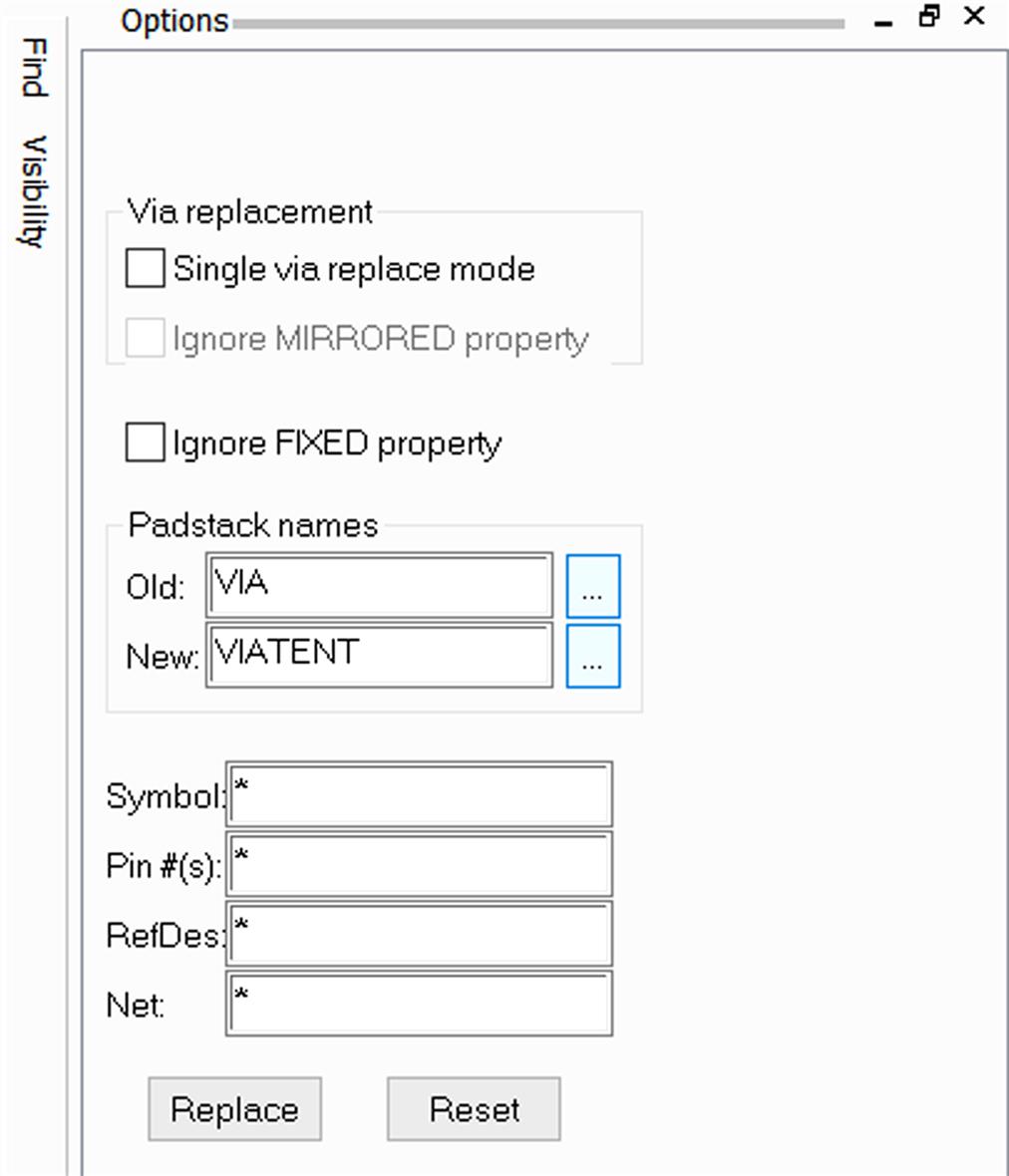
If for some reason the wrong via was used, you can change it. To change placed via types, select Tools → Padstack → Replace from the menu bar. Display the Options tab and, as shown in Fig. 9.170, select the via to be replaced and the new via. Click the Replace button to make the changes take effect.
Once the fan-outs are complete, use the Constraint Manager to fix ground and power nets, and enable all the other nets. Next we route critical traces before autorouting the board.
Determining critical trace length of transmission lines
Since the controlled-impedance traces are critical, they are routed next. The first step is to determine which traces need to be handled as transmission lines and which ones do not. As mentioned previously the digital-to-fiber interface IC, FO-TX (U2), was modeled after the Analog Devices ADN2530. In the data sheet the digital-signal lines going to the part and the modulation signals leaving the part (going to the laser diode) are to be handled as transmission lines. The digital control lines going to U2 need not be handled as transmission lines. The only traces left to consider are the ones related to the crystal oscillator and the NAND gates.
The literature states that the propagation time, PT, should be less than one half of the rise time, RT (or fall time, FT); that is, PT<1/2 RT. If possible it is better if PT<1/4 RT (see Chapter 6: Printed circuit board design for signal integrity, for more details). So we need to calculate PT for this board layout and look up RT and FT for the oscillator and the NAND gates. Since the crystal is a fictional part here, let us assume that RT=FT=pulse width=1/4 the total period of a 66-MHz square wave. Under that assumption RT=3.8 ns for the oscillator. The typical RT for ALS (Advanced Low-power Schottky) family logic is 1.9 ns.
The critical maximum length can be calculated using the following equation:
(9.1)
where Lengthtrace is the maximum allowed trace length in inches, RT is the signal rise time in picoseconds, k is the safety factor (k=2 minimum), and tPD is the propagation delay of the board material in picoseconds per inch.
The propagation delay for the surface microstrip (see Table 6.6 in Chapter 6: Printed circuit board design for signal integrity) is
(9.2)
using εr=4.2 for FR-4, tPD=137 ps/in., and the critical trace lengths are given in Table 9.10 for various values of k. As indicated, there is no way that the ADN2530 traces can be treated other than as transmission lines, but as long as none of the other traces is longer than 3.5 in., they need not be treated as transmission lines. Note that we are neglecting the length of the cables leaving the board through connector J1, but that is beyond the scope of the example.
Table 9.10
| Maximum Lengthtrace (in.) | ||||
|---|---|---|---|---|
| RT (ns) | k=2 | k=3 | k=4 | |
| 66-MHz OSC | 3.8 | 13.9 | 9.26 | 6.95 |
| ALS logic | 1.9 | 6.95 | 4.63 | 3.47 |
| ADN2530 | 0.026 | 0.095 | 0.063 | 0.048 |

Routing controlled impedance traces
The objective is to design surface microstrip transmission lines with a characteristic impedance of Z0=50 Ω. Using the design equations from Chapter 6, Printed circuit board design for signal integrity, repeated here in the following equation, the width of the trace is calculated as
(9.3)
where, from Fig. 9.158, t=1.35 mil (1 oz copper), h=10 mil, k=87 for 15<w<25 mil (most references use this number—87 is used here), or k=79 for 5<w<15 mil (Montrose offers this option), Z0=50 Ω (the design goal), and the desired trace width in mil w=17.5 mil (17 mil=50.9 Ω).
To specify the width of a net, open the Constraint Manager. Select the Physical tab and select the All Layers icon under the Nets folder. Set the Min trace width to 6 mil and the Max value to 17.5 mil in the Line Width columns for the ModN and ModP nets.
With these settings the traces will be 6 mil by default (good for connections to the small surface-mount pads) but can be as wide as 17.5 mil (which is needed for the transmission lines).
Next the transmission lines are routed manually. Choose the Add Connect tool. Select a net on U2 at a point close to the pad to begin routing. Place a vertex just outside the place outline by left clicking once (this short, narrow trace allows for a thermal relief during reflow but is too short to interfere with the trace impedance).
With the vertex in place, we now want the 17.5 mil trace. To change the trace width, display the Options pane and enter 17.5 in the Line width: box, as shown in Fig. 9.171. The trace attached to your cursor should now be the correct width, and you can continue routing to the laser diode pin. Repeat this process for the other net. Fig. 9.172 shows the completed transmission line.


Note that, because of the pin-out of the component and the lead spacing of the diode, the lengths of the traces may not be equal (which is recommended in the data sheet). You can use the Show Element tool to measure the lengths of the traces. Fig. 9.173 shows a comparison of the two traces and reveals that the top trace (MODP) is about 58 mil longer than the bottom trace (MODN).

If we want the trace lengths to be within a certain tolerance, then we need to reroute the shorter traces to include extra length (using trombones, accordions, or sawtooths) or change the position or orientation of either or both components. As an example Fig. 9.174 shows U2 rotated 45 degrees and relocated. The trace lengths in this configuration are equal to within 0.01 mil.

To rotate a part 45 degrees, select the Move tool, display the Options pane, and select 45 in the Angle: selection list. Select the part (make sure the Symbols box is checked in the Find filter pane), right click, and select Rotate from the pop-up menu. Move the cursor around to rotate the part. When the part is in the correct rotation, left click, move the part to the correct place, and left click again to place the part.
Maximum neck length
When routing traces with varying widths, DRC errors may result because a trace has been “necked down.” To clear maximum-neck-length DRC errors, open the Constraint Manager, select the Physical tab, and select the All Layers icon under the Physical Constraint Set folder. Change the DEFAULT Maximum Neck Length as necessary (e.g., 40 mil) to eliminate the DRC errors.
Moated ground areas for clock circuits
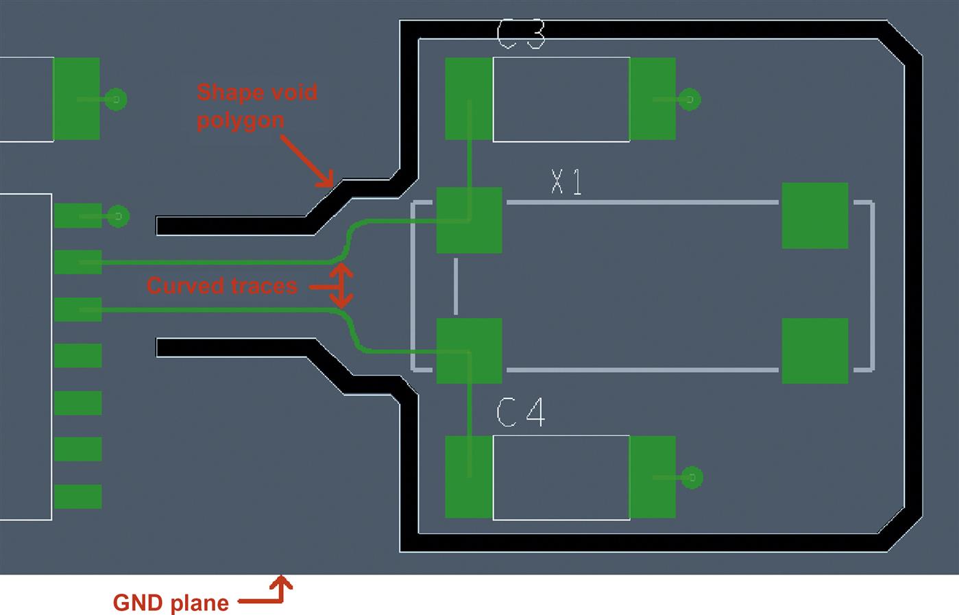
The oscillator is routed next. In many applications a moated ground plane around the clock circuitry is recommended to prevent stray ground currents from affecting other circuits. Before adding the moated ground area around the oscillator, the traces should be routed so that the size of the required ground area is known. Begin by enabling all the nets associated with the clock circuitry (set Rats on). Route the traces manually. Fig. 9.175 shows the routed, curved clock traces (along with the moat, which is described later).
Routing curved traces
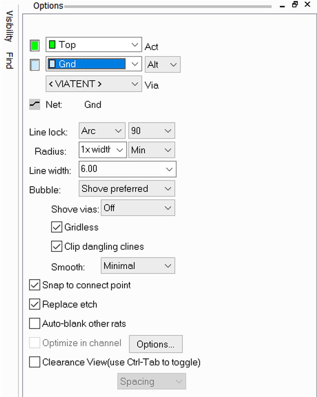
Notice that the traces between the crystal (X1) and U1 are curved. While they are not necessary, the curved corners are used here as a demonstration. To route curved traces, select the Add Connect tool, left click the net near one of the pads on X1, route the trace straight out from the pad about 100 mil or so, and place a vertex by left clicking. Display the Options pane and select Arc from the Line lock: list (Fig. 9.176). As you move your mouse around, you will see that the trace is a curve instead of an angle. Place vertices to define the curves. You can switch between curves and lines as needed using the Options pane.
The next step is to etch a moat into the GND plane around the clock circuitry (see Fig. 9.175). To etch a moat into a plane, make the GND plane visible, and choose the Shape → Manual Isolation/Cavity → Polygon tool.
In the command window, PCB Editor will ask you to Pick shape or void to edit. Left click on the ground plane to select it (it will become highlighted). Create the void by picking void coordinates with the left mouse button. To define the shape shown in Fig. 9.175, 32 pick points were required. When you get to the last pick point, right click and select Complete from the pop-up menu.
Make sure to leave a “bridge” attached to the main ground plane. The bridge should be wide enough to include the ground pin and the area under the clock traces on U1. The local ground area under the clock circuitry must be attached electrically to the rest of the ground system, but the moat is used to “corral” the ground currents back to the ground pin on the IC. Ground areas (and moats) will be placed on the Top and Bottom layers, and ground stitching will be used on all Ground planes; but before that is performed, the rest of the board needs to be routed.
Notice that you can also add the void in all layers at once by creating the shape in Route Keepout/All subclass.
Disable and lock all routed traces (use the Constraint Manager to turn on the Fixed parameter). Enable the remaining unrouted nets and set the routing grid to 25 mil (Setup → Grids, All Etch Spacing:). Autoroute the board (Route → PCB Router → Route Automatic…, Routing Passes: Route and Clean on, Fanout off). Fig. 9.177 shows the result. Many of the traces have wandered around due to poor usage of the gates (as assigned on the schematic), particularly around the areas marked 1 and 2. Note also that, at area 3, two traces were routed over gaps (the moat) in the Ground plane. As described in Chapter 6, Printed circuit board design for signal integrity, we do not want to allow this, as it will increase the loop inductance and introduce EMI issues. To fix these two problems, we now look at how to perform pin and gate swapping and how to define a route keep-out area to prevent the autorouter from routing traces over the moat.

Gate and pin swapping
Two methods can be used to swap gates and pins. The first is to swap the gates (or pins on a gate) on the schematic page and run an ECO to PCB Editor. The second method is to swap pins in PCB Editor and back annotate the changes to Capture to update the schematic.
The second method described is demonstrated here. Before doing the swap, save the design (or save as a new .brd file) so that the preswap design can be recovered if something goes wrong.
The first task is to unroute the gates. Make sure all gate nets are enabled, and all other nets are disabled and fixed. Select the Delete tool and drag a box across multiple nets to rip up more than one trace at a time.
Before a swap can be made, you need make sure pins are swappable in Capture. To verify that they are swappable, go to the schematic page, double click on a pin, select <Current Properties> from the filter list; its Swap ID will be −1 if it is not swappable, and it will be 0 or a positive number if it is swappable. If pins are not swappable, you need to change the property of the pins in the part definition in Capture.
To make pins swappable, go to the schematic in Capture, left click on the logic gate you want to make swappable, go to the Edit menu, and select Part. The part editor will be displayed. In the part editor, open the Property Sheet, press Edit Pins button, and in the Pin Group column, check that the swappable pins have identical numbers (see Fig. 9.178). So far any pin within the gate is available for swapping with any other pin of the same gate if it has the same Pin Group number. Click OK to dismiss the spreadsheet.

In the homogeneous part, all gates are identical, and Capture will automatically put the same integer number in the same input pin on all of the gates. Notice that in any homogeneous part all gates will be equally available for swapping with any other gate in that IC. But if the part is created as heterogeneous then every section differs from others. If you want to make some pins of one section of heterogeneous part to be swappable to some pins of other section, you can add the SWAP_INFO property to such part defining which sections may swap the pins which have the same Pin Group number. For example, SWAP_INFO=(S1), (S2+S3) will mean that Sections 2 and 3 may have some pins which you can swap not only within the section but also between these sections.
To save the changes, click the X in the upper right-hand corner to close the part editor. When Capture asks if you want to change only the one or all of them, choose Update All. Choosing Update Current will cause problems with the netlister, because when you change a part with the part editor, the link between the part and the library from which it came will be broken, and the part will be given a modified name with a suffix (e.g., 54ALS00A will be renamed to 54ALS00A_1). Every time you modify a gate, the suffix is incremented. So if you modify a gate and choose Update Current, only that gate will be modified, and its suffix will be different from the other gates within the same IC package. You can check this by selecting the parts, right clicking, and selecting Edit Properties from the pop-up menu. Select <Current Properties> from the filter list and look at the Source Package cells for the individual gates. If gates from the same IC have different names (suffixes), the netlister will fail during an ECO (check the netlist.log file for details if this happens). If you choose Update All, then all gates in that IC will be given the same suffix. Gates contained in different ICs will not be changed (or renamed) by Update All, so if you want them to be swappable, you will need to modify them as well. If the parts within a package end up with different names, you cannot modify a single part to change its name to match the others, because Capture will increment its suffix to one greater than the highest suffix in the package, so they will always end up being different. The good way to fix it is to use the Replace Cache command in the Design Cache folder of the Project Manager pane.
Repeat the steps to make pins swappable for pins 10 and 11 on U1.
If you have had to modify parts a couple of times, a record of each change is maintained in the Design Cache folder in the Project Manager pane. This is not a problem, but you can remove the outdated parts from the Design Cache by selecting (left click on) the Design Cache folder then selecting Design → Cleanup Cache from the menu bar.
After you have made gates/pins swappable, you need to perform an ECO to let PCB Editor know that the pins can be swapped.
Once the ECO is complete and the board design is open, swapping is accomplished through the Place menu. The Place menu offers two swap options, Swap and Autoswap, and in each of the two options are additional options. In short the difference between the two options is that the Swap option gives you specific control over pin, function, and component swapping actions; while the Autoswap option allows PCB Editor control over swapping actions (with some input from you). We first look at the Swap option.
Using swap options
Pin swapping
In this example, we use the Swap option to manually uncross the two nets between U1 (pins 10 and 11) and U2 (pins 11 and 12). To perform a manual pin swap, select Place → Swap → Pins from the menu bar. In the command box, you will see Pick a pin you wish to swap. Pick pin 10 on U1. Then in the command box, you will see
last pick: 3500.00 3200.00
Pick a pin you wish to swap from those that are highlighted.
The package to which the pin belongs will have the other pins highlighted that were set in Capture with the same pin group number. Select pin 11 on U1. Then you should see
last pick: 3500.00 3200.00
Pick DONE/NEXT or pick the first pin of the next swap.
Right click and select Done from the pop-up menu. The nets should now be swapped between the two pins and no longer be crossed. A back annotation will be performed at the end of this section to show the effects of the pin swap in Capture.
You can perform pin swaps on logic gates too. When doing so, PCB Editor will allow you to swap pins only within a single gate and only pins that are of the same type. For example, if you pick pin A on a NAND gate (an input pin), it will allow you to swap it only with pin B on the same gate. You cannot swap pin A with any pin on another gate (even if it is on the same IC), and you cannot swap it with pin Y (the output) on the same gate, because pins A and Y are different types of pins.
Function (gate) swapping
If you need to swap an entire gate (e.g., U3A for U3C) and not just pins within a gate, then you use the Swap → Functions option. To swap two gates (and therefore their pins), select Place → Swap → Functions from the menu bar. In the command window, PCB Editor will instruct you to Pick a function you wish to swap.
In this example, select pin 1 on U3 (this is input pin A on gate A). All the pins on U3 will become highlighted and the command window will display
last pick: 2400.00 2700.00
Pick a function to swap with from those highlighted …
Select pin U3.13 (this is input pin B on gate D); the command window displays:
last pick: 2600.00 2700.00
W- (SPMHA2-12): Pick NEXT/DONE or pick the first function of the next swap.
Right click and select Done from the pop-up menu. The rat’s nest lines that were connected to gate A will now be connected to gate D, and the pins will be utilized in the best way to minimize length of the rat’s nest (referred to as virtual wire length by the Autoswap tool).
Swap → Components does not perform gate or pin swapping, it just physically swaps (trades) the locations of two components on the board. The components do not even have to be the same type or be “swappable.” To perform a component swap, select Place → Swap → Components from the menu bar. The command window will not ask you for anything, but left click one of the parts in the design (it will become highlighted) then left click another part. The two parts will immediately trade places. To undo the component swap, right click and select Oops or Cancel from the pop-up menu.
Back Annotating the swap operations to Capture
If you are working through these examples on your own board design, you can perform a back annotation to see the effects of the gate and pin swapping on the schematic. To perform a back annotation, the steps are to be followed:
- • Save your PCB design and exit from PCB Editor.
- • In Capture schematic project select the design icon in the Project Manager window, select Tools → Back Annotate from menu and choose the proper file using PCB Editor Board File: browse button.
- • Check the path and name of the Output File where the result of back annotation will be stored.
- • Check the path where the PCB Netlist is located and press OK.
When you go back to your schematic, it should be updated with the new information, as shown in Fig. 9.179 (compare this to Fig. 9.156).
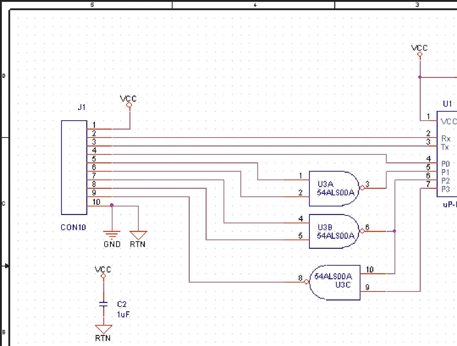
In the case of the pin swap on the microcontroller (U1), pins 10 and 11 were actually moved on the part definition (and a suffix was added to the parts name, as described previously) while the nets were physically unaltered (see Fig. 9.180). This is obviously different from the way pin swaps look in PCB Editor and can be easily missed. If you or another designer replaces this modified part with the original from the library and an ECO is performed, the pin swap will be effectively undone. Another point to consider in an example like this is that any software written for the microcontroller would have to be changed to accommodate the pin swap.
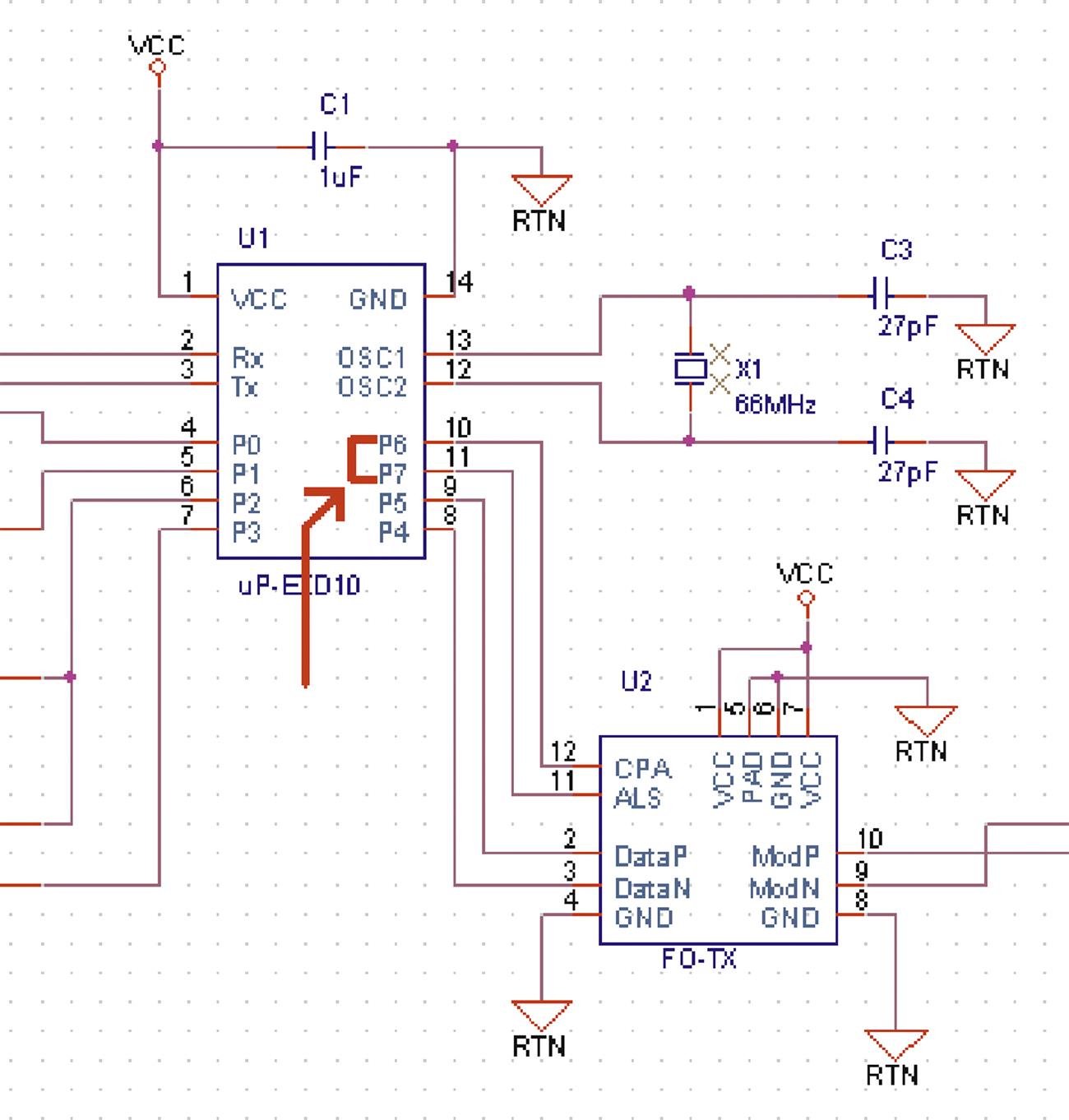
Using the Autoswap option
In using the Autoswap option, you basically let PCB Editor figure out the best gate usage and pin connections then back annotate the results to the schematic. You do have some control over the swapping action. From the Autoswap menu, you can have PCB Editor work the whole board design, a room, or a selection window. After you select the type of autoswap you want to do, you select Place → Autoswap → Parameters to execute the swap. Examples of each follow. Once you perform an autoswap, you cannot Undo it, so to try all the autoswap types on this small design, you can try a swap and close the PCB design without saving it (and without doing a back annotation) then reopen the board design to try a different one.
Autoswapping an entire design
To have PCB Editor review and autoswap an entire board design, select Place → Autoswap → Design from the menu bar. Then select Place → Autoswap → Parameters… to display the Automatic Swap dialog box shown in Fig. 9.181.
The numbers represent the time limit (in minutes) for each pass. After a pass PCB Editor records the virtual wire length for each net and compares the lengths to the previous pass. PCB Editor will continue trying to shorten the wire lengths until all passes have been completed or the wire lengths cannot be made any shorter. By default only two passes are enabled. Passes with a 0 time limit are disabled.
The Inter-room option allows or prohibits PCB Editor from attempting to shorten the wire lengths by swapping gates between different rooms.
You can specify more or fewer passes and change the time limit depending on the complexity of your design. You can see what PCB Editor attempted to do during each pass by reading the swap.log file that PCB Editor generates after a swap operation. The swap.log file is located in the same file folder as the board design.
To begin the autoswap, click the Swap button. PCB Editor will look over all the components and nets and automatically swap all gates and pins in a way that will result in the shortest traces. Note that gates that were not placed somewhere on the design will not be considered for swapping and neither will gates with “NC” markers on pins or pins connected to nets that are fixed or nets that have a No Ripup property assigned in Constraint Manager. If you want unused gates that were not placed on the schematic to be considered for gate swapping, place them on the schematic and leave the pins floating. After the swap and subsequent back annotation, you can apply NC pins and delete unused gates.
Autoswapping a Room
You can restrict how much the design PCB Editor is allowed to modify by defining rooms around a component or groups of components and telling PCB Editor to work on only the rooms you want swapped. To use this option, you must have rooms defined (review Design Example 1 to see how to set up rooms). Once rooms are defined, select Place → Autoswap → Room from the menu bar. The Physical Room Browser will be displayed, as shown in Fig. 9.182. Select the room you want PCB Editor to review and autoswap, and click OK. Then select Place → Autoswap → Parameters… to display the Automatic Swap dialog box, and click the Swap button. PCB Editor will automatically swap all gates and pins in the selected room but will leave the rest of the design alone.
Autoswapping a window selection
You can also restrict how much of the design PCB Editor is allowed to modify by defining a window around a component or groups of components. To use the Autoswap Window function, select Place → Autoswap → Window from the menu. Define the window by clicking your left mouse on the design to define a window corner then drag a box (window) around the components you want swapped, and left click again to complete the window. If you want to define more windows, repeat these steps. When you are finished, choose Done from the pop-up menu. Then select Place → Autoswap → Parameters… to display the Automatic Swap dialog box, and click the Swap button. PCB Editor will automatically swap all gates and pins within the selected window (if swapping results in an improvement) but will leave the rest of the design alone.
Viewing the swap list and the swap log
Once you have made a swap type selection, you can review what PCB Editor will be looking at with a swap list before you actually perform the swap. To display a swap list, select Place → Autoswap → List from the menu. The swap list shows you where PCB Editor will focus during the swapping operation, but it does not give you information about the swap itself. You can obtain detailed swap information by opening the swap.log file generated after a swap is performed. The swap.log file is located in the same file folder as the board design.
Once the swaps have been completed you can rerun the autorouter. Fig. 9.183 shows the results of the autoswap and autoroute. The figure also shows the route keep-out area placed over the ground moat. Notice how the autorouter hugs the keep-out area but does not cross it. Defining a route keep-out area is described next.
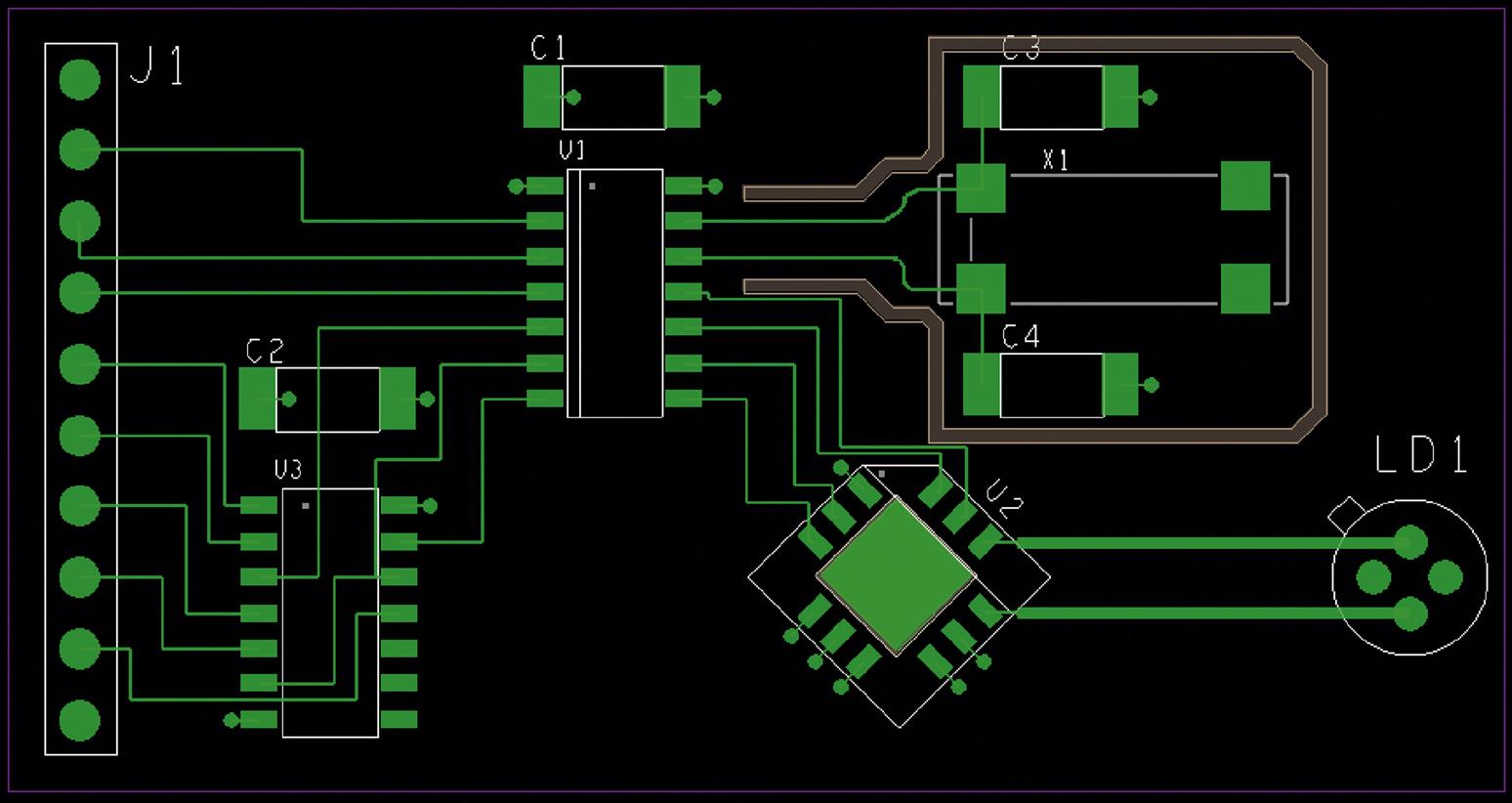
Defining a route keep-out area
 Shape Add button
To define a route keep-out area on your board, begin by making the Route Keepout class active on the Options pane. In the subclass list, you can choose any of the layers. In this example, select the All subclass to place the keep-out on all layers simultaneously. Next, select the Shape Add button, , on the toolbar. Draw a polygon on the Route Keepout / All class/subclass that matches the moat in the Ground plane. This will keep the router from routing any traces on Routing (conductor) layers and will also create a void in the VCC plane layer similar to what the void shape did on the Ground plane (see Fig. 9.175). The keep-out also works if you pour a copper ground area on the Top and Bottom layers, such as the one demonstrated in Example 3.
This completes the Example 4 design.
Positive planes
As we saw in the previous design examples, keeping track of the necessary details to use negative Plane layers can be a bit of a task (making flash symbols, modifying padstacks, etc.). Negative planes are used because they have been used historically. One of the reported advantages of using negative planes is that the artwork files are smaller than for positive artwork files. With the current PC speed and memory capacity, file size is less of an issue. Another argument for negative planes is a shorter processing time for negative planes at the manufacturer’s end. That certainly was true for vector plotting with the flash lamps, but for current photoplotting equipment it has become less of an issue. Yet another argument for negative planes is that, during the board design, the positive planes can be distracting and result in slow drawing regeneration. But PCB Editor displays the negative planes in the positive view (“what you see is what you get” mode) anyway, and you can easily turn off the Plane layers. In addition, the author is aware of some designers who use positive planes for most of their work. That being the case and for the sake of completeness, we look at a very simple design to demonstrate how to use positive planes and take care of the corresponding details.
The circuit for this example is shown in Fig. 9.184. As shown, the circuit consists of only two resistors. We focus on the Plane layers that will be used by the VCC and GND nets, so this simple circuit suffices.
As with the previous design examples, the netlist is created and PCB Editor is launched. A board outline is drawn and the parts placed. The next step is to define the layer stack-up.
In the previous design examples the Ground and Power planes were defined as negative Plane layers. In this example, we use positive planes. The layer stack-up is shown in Fig. 9.185. As indicated the layer stack-up is similar to the other design examples except that the Negative Artwork boxes are unchecked.
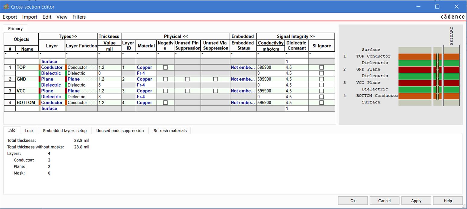
A positive plane layer should still be specified as PLANE rather than CONDUCTOR so that the autorouter does not try to route traces on that layer. Routing traces on Plane layers (particularly GND planes) results in slots in the plane, which disrupts the return paths for signals on Routing layers and can lead to signal integrity issues. Setting the type as Plane prevents this.
Once the layer stack-up is specified, the next step is to draw the copper areas on the planes. The process is identical to the previous examples. Select the Shape Add tool, select the GND or VCC subclass in the Etch class, and draw a dynamic copper area attached to the appropriate net.
Unlike with negative planes, you do not have to enable the Thermal Pads setting in the Design Parameters dialog box to see the thermals. Fig. 9.186 shows the two resistors and the VCC plane. Note that R1 is connected to the plane with a thermal relief that was automatically generated by PCB Editor. The padstacks used in this design are native to the symbols library and have no thermals assigned to them. This result is similar to the Ground plane placed on the Top layer in Example 3.

A close-up inspection of the padstack reveals that the inner pad is indeed 55 mil, but the diameter of the clearances (outer diameter of the thermal relief) is only 65 mil (leaving a space of only 5 mil between the pad and the copper area). So, on a positive plane, neither the thermal relief diameter nor the Anti Pad diameter in the padstack definition determines the diameter of a clearance or the outer diameter of a thermal relief.
Since PCB Editor automatically generates the thermal reliefs, a question arises as to how it determines the thermal relief dimensions. The answer was described briefly in Example 2. The space between the copper area and the padstack is determined by the spacing constraints set in the Constraint Manager, and the spoke width is determined by the trace width setting in the Constraint Manager. If we change the shape-to-pin spacing constraint to 10 mil (see Fig. 9.187), the thermal and clearance areas should increase. And if we change the trace width constraint to 10 mil (see Fig. 9.188), the spoke width should increase.

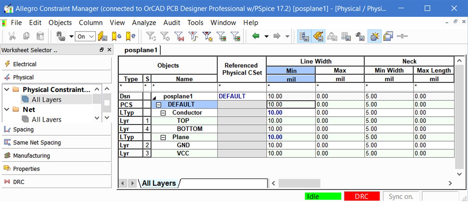
Fig. 9.189 shows the difference between (A) the default constraints and (B) the result of changing the trace width and spacing to 10 mil—the spoke widths and the void width are wider.

Besides the constraint settings in the Constraint Manager, you also have control over thermal reliefs on positive planes using the Design Parameter Editor. As shown in Fig. 9.190, additional parameters can be set by selecting the Shapes tab and clicking the Edit global dynamic shape parameters button. At the Global Dynamic Shape Parameters dialog box, you can control the rotation (Orthogonal, Diagonal, or Full contact, etc.), the number of connects (spokes), and set fixed or scaled spoke widths (relative to the trace width constraint).
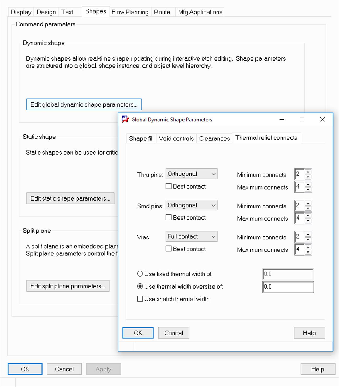
One thing that is different about this plane and a typical negative plane is that the pads not connected to the planes are present, whereas with the negative planes, they are absent. Typically, it is desired that the unused pads on Plane layers are removed. Although the pads cannot be removed in the design mode, they can be removed during the artwork production.
Positive plane artwork production
Artwork production is covered in detail in Chapter 10, Artwork development and board fabrication, but we touch on it here. To create Gerber files select Export → Gerber… menu. The inner pads can be removed on positive planes during the artwork production, provided that three conditions are met: (1) the Suppress unconnected internal pads option needs to be selected in the Padstack Editor’s Options tab (see Fig. 9.191), (2) the Suppress unconnected pads option needs to be checked in the Artwork Control Form, and (3) the film Plot mode: needs to be processed as Positive artwork (also in the Artwork Control Form, as shown in Fig. 9.192).

The IPC-2221B (2012) standard specifies that unconnected pads on routing layers should be maintained, but unconnected pads on Plane layers can be removed, so when using positive planes, suppress unconnected pads on only the Plane layers and leave the option unchecked for Routing layers.
Fig. 9.193 shows the VCC layer photoplot artwork for this design (silk-screen and other layers not shown). The figure shows that the unused pads were removed as intended. Artwork verification is described in detail in Chapter 10, Artwork development and board fabrication.

Positive versus negative plane file sizes
It was mentioned at the beginning of this section that it is commonly held that the positive plane file sizes are larger than the negative ones. Let us take a look at the file sizes of the resulting artwork for this example. The GND plane artwork for this design in the positive image is 54 lines of Gerber code at 1.15 kB, while the negative artwork file is 128 lines of code at 2.34 kB. So, at least for this simple design, the positive artwork files are actually smaller than the negative files (as generated by PCB Editor anyway).
Pros and cons of using positive versus negative planes
In general, there are two drawbacks to using positive planes. The first is that, in the padstack definition, the Suppress unconnected internal pads option must be set for every padstack in the design for the artwork to be produced correctly. However, it is much simpler to do that than to make and assign thermal flashes for the padstacks. The second potential drawback is that constraints set for trace width and spacing affect the thermal relief geometry (possibly adversely), whereas thermal flashes on negative planes are fixed, and once they are engineered, they are unaffected by changes made in the Constraint Manager. But the latter potential drawback can be mitigated to some extent by using the Global Shape Parameters settings as described previously.
The bottom line though is that, when using OrCAD PCB Editor, positive planes are easier to implement than negative planes as long as the layer stack-up and thermal relief design do not have to be highly engineered.
Design templates
Making a custom Capture template
If you design a lot of projects that are similar to each other, setting up a project template in Capture can be a real time saver and can help eliminate errors by reusing known good project setups. Project templates can be used only when setting up a project through the Analog or Mixed A/D option from the New Project dialog box. However, since you can make a PCB design from either the Analog or Mixed A/D option or the PC Board Wizard option, you can still take advantage of creating your own Capture templates for PCB design projects.
To make a custom Capture project template, start a new Analog or Mixed A/D project; set it up with power supply and ground symbols, connectors, or whatever you want; then save it in the OrCAD tools/capture/templates/pspice folder with the other templates. It will automatically be added to the templates list, so that you can select it the next time you start a new project.
Making a custom PCB Editor board template
As with the Capture templates, if you design a lot of PCBs that are similar to each other, setting up a custom PCB Editor board file (.brd) can save a lot of time and eliminate many manufacturing errors by reusing known good PCB setups.
To make a custom PCB template start PCB Editor, begin with a new board design by selecting File → New from the menu. At the New Drawing dialog box, enter a name for the template and select Board from the Drawing Type: list, as shown in Fig. 9.194. The Board Wizard will be demonstrated later, after a board template and technology file has been developed.

If you see Create a New Design dialog box, select the desired Units, Sheet Size, Accuracy and Extents, and click OK. When the board is opened, use the Design Parameters dialog box to set up the basic design parameters, including
Display tab:
Display plated holes
Display thermal pads
DRC marker size
Design tab:
Design size
Design extents
Shapes tab:
Edit Global Dynamic shape parameters (RS274X for artwork format)
Route tab:
Add connect defaults (trace width and angles)
Create Fanout parameters
Manufacturing Applications tab:
Edit silkscreen parameters
When the parameters have been set, click Apply then OK to dismiss the dialog box.
In addition to setting up previous parameters, the following items can also be set up:
- • Default grid settings (Setup → Grids).
- • A default layer stack-up using the Cross-section Editor dialog box.
- • A board outline (select Outline → Design from the menu).
- • Default artwork folders using the Artwork Control Form.
- • A default, custom color scheme and layer visibility using the Color Dialog box.
- • Design constraints using the Constraint Manager. Default settings might include the default trace width (Physical tab) and the default trace spacing (Spacing and Same Net Spacing tabs).
Once all of the design parameters and constraints have been established, save the board.
You can also save the Constraint Manager settings in a separate technology file that can be imported into any board. This is described in the next section.
To reuse the board template, assign it as the Input Board File: during the netlist creation in Capture, as shown in Fig. 9.195. The new board will inherit all the template board properties.
Making a custom PCB Editor technology template
If you often design boards with similar design constraints, you can save them in a board template. You can also save the Constraint Manager settings to a stand-alone technology file, so that, if you start a new design that is not based on the board template, you can still reuse the design constraints by importing the technology file.
To create a technology file, start from a board template or an active board design that has the constraints you want to be able to reuse. Open the Constraint Manager and select File → Export → Technology File… from the menu. Save the filename.tcf file in a folder that you can easily access for future designs.
When you start a new board and want to load the technology file, select File → Import → Technology File… from the Constraint Manager menu. The technology file will replace the existing constraints and layer stack-up with the setup saved in the technology file.
Using the board wizard
Over time you will likely develop several board characteristics that you have used but not every board uses all of them. For example, you might have two or three board outlines you often use, but the layer stack-ups are different from one board to the next. Perhaps you have different technology files you use and have several mechanical symbols or drawing symbols that you need to select from, but they also vary from board to board. Rather than make a board template for every possible combination of these characteristics, you can save each of the characteristics and symbols in a library and use the Board Wizard to select specific characteristics and combine them into one new board design. The Board Wizard allows you to reuse your favorite board characteristics while keeping your template library more easily organized.
When you start a new board, the wizard will look for templates, technology and parameter files in the current working directory where you start the process but will look in the symbols library for mechanical and drawing symbols. Before you begin, make sure that any mechanical and drawing symbols you plan on using are in the symbols library and any board templates, technology and parameter files you will use are copied to the file path where you are setting up the new board. The board parameter file may contain the design settings, color settings, text sizes and/or other PCB Editor parameters. To save the parameter file select Export → More → Color/Board Parameters.
To begin a new board using the wizard, start PCB Editor and select File → New from the menu. At the New Drawing dialog box, enter a name and path for the new board design and select Board (wizard) from the Drawing Type: list, as shown in Fig. 9.196, and click OK.
The Board Wizard dialog box will be displayed, which provides an introduction to the board wizard. Click the Next button to continue.
The next step is to load a board template (name.brd) if you have one. To load the board template, select the Yes radio button then click the Browse… button to locate the file (see Fig. 9.197). Remember that the board template needs to be located in the OrCAD symbols emplate directory path, or the wizard will not be able to find it. At the Board Wizard Template Browser dialog box, select the board template on which you want to base the new board, then click OK to dismiss the Browser dialog box. Click the Next button to continue to the next step.
Next you can load a technology file (name.tcf) and a parameter file (name.prm). A technology and/or parameter file loaded by the wizard will override the file originally loaded with the board template. If you want to keep the original technology or parameter file, select the No radio button and click the Next button to continue to the next step. Otherwise, to load a different file, select the Yes radio button and click the Browse… button to locate the file, as shown in Fig. 9.198. Remember that copies of the technology file and parameter file need to be located in the directory path where you are setting up the board, or in the folder defined by techpath and parampath in user preferences, otherwise the wizard will not be able to find them. At the File Browser dialog box, select the file you want to use and click OK to dismiss the Browser dialog box. Click the Next button to continue to the next step.
In the next step, you can load a drawing file or mechanical symbol (Fig. 9.199). If you have no drawing or mechanical symbols you want imported into the board, select the No radio button and click the Next button to continue to the next step. Otherwise select the Yes radio button and click the Browse… button to locate the file. At the Board Wizard Mechanical Symbol Browser dialog box, select the symbol you want to add to the board then click OK to dismiss the Browser dialog box. Click the Next button to continue to the next step.

With the next step, you can elect to import the selected files right away or wait until the last step in the wizard process, see Fig. 9.200A. Typically you can import the data right away. Click the Next button to continue to the next step.

At the following step, Fig. 9.200B, you can specify the origin of the new board drawing. Click the Next button to continue to the next step.
The next step allows you to specify whether or not to generate default artwork films, Fig. 9.201A. Click the Next button to continue to the next step.

At the next step you can generate negative internal layers for power planes, and after clicking the Next button you will be able to set up the minimum line width and spacing, and to select the default via padstack (Fig. 9.201B). The succeeding step will allow you to specify the Route Keepin and Package Keepin distance from the board edge.
At the final step in the process click the Finish button to complete the wizard and open the board design.
When you finally get to the new board design, you can either import logic data from a previously generated netlist (Import → Netlist) or save the board design as a board template and use it as an input file when creating a netlist from a new design in Capture.
Moving on to manufacturing
The design examples included here are to provide an overview of the basic steps in the board design processes and introduce the various tools you can use to design different types of boards. These examples were not designed with manufacturability in mind, as that is another subject, which encompasses additional things to consider and would have made the examples overly cumbersome. Chapter 10, Artwork development and board fabrication, combines design for manufacturing topics introduced in Chapter 5, Introduction to design for manufacturing, with design processes introduced here.