Artwork development and board fabrication
Abstract
Developing artwork for the board design was briefly introduced in one of the chapters. Here we look at this step in greater detail. To illustrate the process, we will create and route a new simple PCB project, place mounting holes and assembly fiducials. Then we will setup the artwork (Gerber) and NC drill files. We will see how the PCB Editor auto-silkscreen tool is working, to prepare the high quality silkscreen photoplot data. We will generate Gerber, Drill and Mill manufacturing files, as well as an assembly Pick & Place program.
Keywords
PCB; DRC; solderpaste; silk screen; fiducials; NC drill; Gerber; RS274X; ODB++
Developing artwork for the board design was briefly introduced in Chapter 2, Introduction to the printed circuit board design flow, by example. Here we look at this step in greater detail. To illustrate the process, we will create and route a new simple PCB project, place mounting holes and assembly fiducials. Then we will setup the artwork (Gerber) and numeric control (NC) drill files. We will see how the PCB Editor auto-silkscreen tool is working, to prepare the high quality silkscreen photoplot data. We will generate Gerber, Drill and Mill manufacturing files, as well as an assembly Pick & Place program.
Schematic design in Capture
As with the previous examples, we use a simple circuit to minimize those details and allow us to focus on the board layout and manufacturing steps. The circuit (shown in Fig. 10.1) consists of a 10-pin printed circuit board connector (J1), a bypass capacitor (C1), a logic IC (U1), load resistors (R1 and R2), and two plated mounting holes that electrically connect the ground plane to the PCB’s mounting bracket. Once we move the design to PCB Editor, two more mounting holes will be added, which are nonplated and electrically isolated from the board. The two types are used so that, when we generate the drill files, you will be able to see the differences between the two types of drill holes.

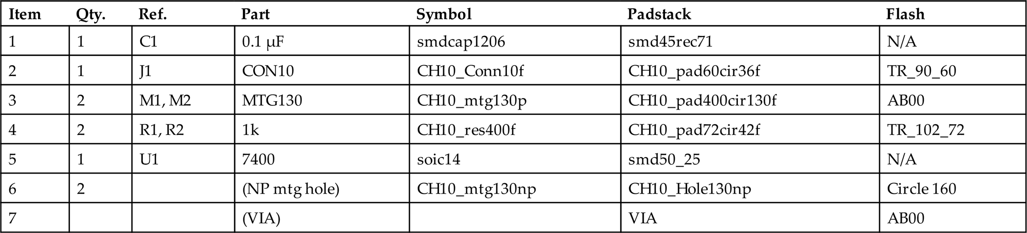
Table 10.1 shows the bill of materials for this design. Only the footprint symbol for U1 (soic14) is from the native PCB Editor symbols library. The footprint for C1 was made in the footprint design example from Chapter 8, Making and editing footprints; the electrically connected mounting hole, mtg130p, is a custom symbol; and the remaining symbols are modifications of existing footprints. The footprint symbols are on the website for this book, and you need to copy them (and the associated padstacks and flash symbols) into the PCB Editor’s symbols folder. You also need the mtg130np mechanical symbol, which is included on the website in the same folder.
Table 10.1
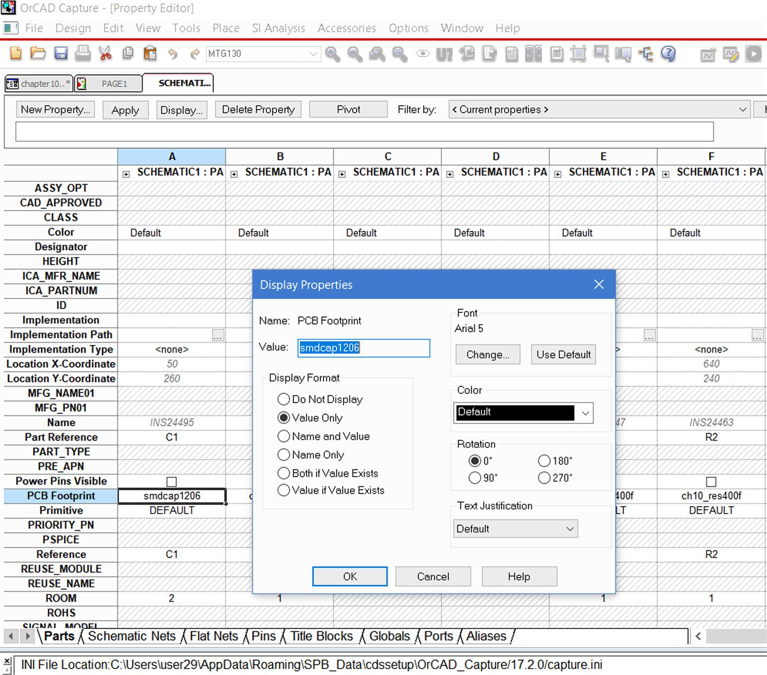
The footprint names for each of the components are shown on the schematic. To display component information on the schematic, double click the part to display the Property Editor spreadsheet (see Fig. 10.2). Select the cell (row or column) that contains the information you want displayed. Click the Display… button at the top of the spreadsheet to show the Display Properties dialog box. Select one of the display formats and click OK. Click the Apply button at the top of the spreadsheet and close the spreadsheet.
Once the schematic is completed, generate a PCB Editor netlist as described in Chapter 9, PCB design examples.
The board design with PCB Editor
Routing the board
Fig. 10.3 shows the routed board. The stack-up consists of the top and bottom routing layers and the VCC and GND plane layers. The stack-up was defined and the traces routed using the procedures described in the Chapter 9, PCB design examples. The padstacks used in the footprint symbols for J1 and the two resistors (R1 and R2) have flash symbols already defined, so they should automatically show their thermal reliefs when the plane layers are visible.
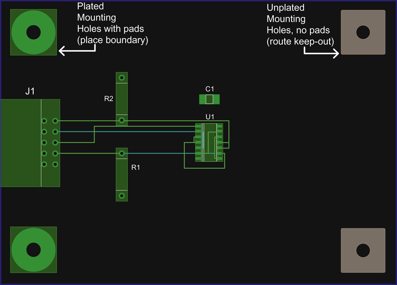
Along with the components and routed traces, the board contains four mounting holes. The two on the left side of the board are the ones included on the schematic and are component symbols (CH10_mtg130p.psm) with plated padstack holes (CH10_pad400cir130f.pad). The f indicates that the flash symbols have been predefined. They are placed on the board using the same procedure used for placing the other components.
The two on the right side of the figure are mechanical symbols (CH10_mtg130np.bsm) with nonplated padstack holes (CH10_Hole130np.pad) and are added to the board from within PCB Editor using the following steps. Make sure you have copied CH10_mtg130np.dra, CH10_mtg130np.bsm and CH10_Hole130np.pad into your PCB Editor symbols library.
Placing mechanical symbols
Mechanical symbols for mounting holes
To place the mechanical symbol mounting holes, select Place → Mechanical Symbols from the menu bar or select the Place Manual button on the toolbar. At the Placement dialog box (see Fig. 10.4), select Mechanical symbols from the Placement List. Click the Advanced Settings tab and make sure that the Library option is checked. Select the Placement List tab again, and check the box beside the CH10_MTG130NP icon. Move your pointer to the design area; the symbol will be attached to it. Left click to place the mounting hole. Recheck the box for each hole you want to add to the board design. Click OK to dismiss the dialog box.

Since the plated holes are footprints, they contain a place boundary like any other component, but on this footprint place boundaries were added to both the top and bottom layers. The symbol was designed that way so no components are allowed to be located near the holes and cannot contact the mounting hardware (standoffs, washers, or nuts, say).
The unplated holes are mechanical symbols. They contain place boundaries on the top and bottom (not shown in the figure) for the same reason, but they also contain route keep-out areas (Route keepout/All). The keep-out areas are needed so that traces cannot be routed under mounting hardware or across the unplated hole (and subsequently drilled away). The design rule checker (DRC) may not detect such a situation, because the Constraint Manager does not know about the mounting hardware that will be put into the hole, and there are no pads against which to maintain spacing rules.
Mechanical symbols for fiducials
Fiducials are marks or objects used for aligning the board with solderpaste stencils and pick and place machines.
Stencils are thin stainless steel plates or sheets through which solderpaste is squeegeed onto the board. The thickness of the stencil establishes the thickness (and therefore the amount) of the paste applied to the pads. The stencil manufacturer uses the pastemask file to fabricate the stencil.
Fiducial objects are placed at particular coordinates on both the board and the stencil, and optical equipment is used to align the stencil to the board during application of solderpaste.
During pick and place operations the fiducials on the board are used to precisely identify the location and orientation of the board so that the components are accurately placed into the solderpaste.
On the circuit board the fiducial is typically a copper mark produced during the etch process. Because the fiducials are relied on optically, the soldermask is usually removed at the fiducial location. Since the fiducial needs to be visible through the stencil, an exact copy of the fiducial needs to be included with the pastemask pattern. A fiducial object then requires etch, soldermask, and pastemask elements.
Note: Many of the native PCB Editor footprint symbols do not contain pastemask elements; so you need to add them to the footprints if you plan to fabricate a stencil and use pick and place processes to populate your board.
We next look at how to make a fiducial. Ideally we want the fiducial to be a symbol that is an element of the board rather than a component. So we want to construct the symbol on the classes and subclasses shown in Table 10.2. Unfortunately a pastemask subclass does not exist under the Board Geometry class. So, we will make one. Begin by opening a new mechanical drawing in PCB Editor as described in the mounting hole example.
Table 10.2
| Function | Class | Subclass |
|---|---|---|
| Copper object | Etch | Top |
| Soldermask opening | Board geometry | Soldermask_Top |
| Pastemask opening | Board geometry | Pastemask_Top |
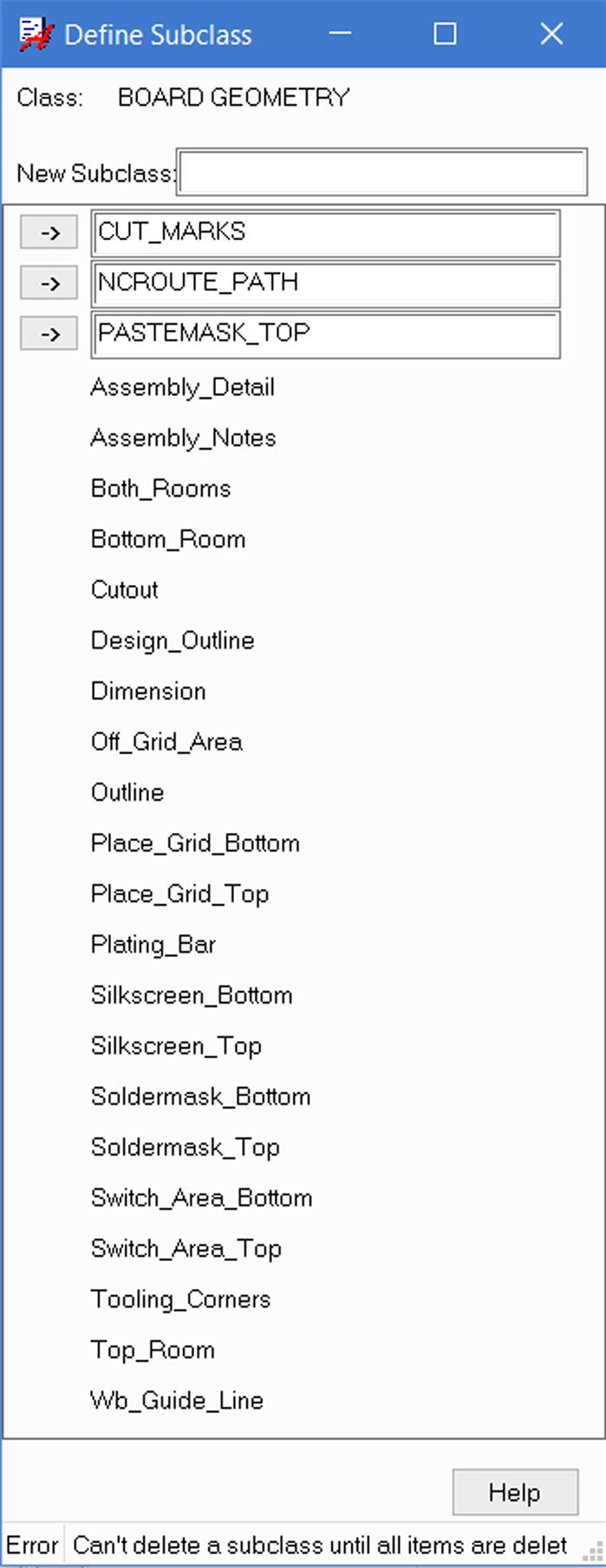
To define a new subclass, select Setup → More → Subclasses… from the menu. At the Define Subclass dialog box shown in Fig. 10.5, select the class where you want to assign the new subclass. For this example, click the box next to Board Geometry.

At the Define Subclass dialog box (see Fig. 10.6), type PASTEMASK_TOP in the New Subclass: text box then hit the Enter key on your keyboard. The new class will be added to the list and displayed in the Options pane and the Color dialog box.
The geometry of a fiducial is typically specified by the user. In this example the fiducial will be a 40×40 mil2. The first step is to place the copper square. Change the All Etch grid setting (Setup → Grids) to 10 by 10 mil. Zoom in to the center of the drawing area (0, 0). Select the Etch/Top class and subclass from the Options pane. Select the Shape Place Rect tool and draw a 40×40 mil box centered at coordinate (0, 0).
Next we draw the soldermask opening. Change the Non-Etch grid setting to 5 by 5 mil. Select the Board Geometry/Soldermask_Top class and subclass from the Options pane. Select the Shape Place Rect tool and draw a 50×50 mil box (5 mil larger than the pad on all sides) centered at coordinate (0, 0).
Finally the pastemask is defined. Repeat these procedures using the Shape Place Rect tool on the Board Geometry/Pastemask_Top class and subclass and draw a 40×40-mil box centered at coordinate (0, 0) directly over the copper pad. Save the drawing to create the .bsm file.
To place the fiducial, use the procedure described for placing a mechanical symbol. Place two or more fiducials on the outer perimeter of the board.
Generating manufacturing data
Manufacturing data include two general types of files: artwork (Gerber) files and NC files (for drilling and milling). These files are made using two or more distinct processes. We begin with the artwork files.
Generating the artwork
The artwork files describe elements of the design and include the Etch, Soldermask, SolderPaste, and Silk-Screen layers.
Most of the manufacturing data are basically present in the board design but not in a format that manufacturers use. The artwork creation process performs that function.
Before we begin the process, one more element needs to be added to the board, a photoplot outline.
Adding a photoplot outline
The board outline generated by the Design Outline dialog box serves as a guide for the designer during the design process, but maybe sometimes it does not contain manufacturing data for the manufacturer. That information may be contained in a photoplot outline.
To draw a photoplot outline, select the Manufacturing class and Photoplot_Outline subclass from the Options pane. From the toolbar, select the Add Rect tool (not the Shape Add Rect button). Draw a rectangle directly over the top of the board outline located on the Board Geometry/Design_Outline layer. A photoplot outline is shown in Fig. 10.7.

Optional artwork items
All the silk-screen elements in the design are associated with the individual components. You can add additional etch and silk-screen markings that are specific to the board. For example, you can use objects (mechanical symbols) on the top or bottom layers to add a company logo or add silk screen to display the board part number or manufacturing date, say, as shown in Fig. 10.7.
Once the board is ready to go, the next step is to generate the artwork files.
Generating the artwork files
Artwork control form
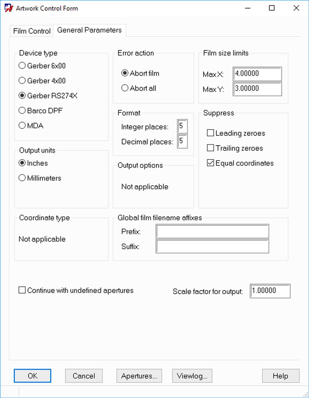
The artwork files are generated using the Artwork Control Form dialog box (shown in Fig. 10.8). To display the Artwork Control Form dialog box, select Export → Gerber from the menu bar or click the Artwork button on the toolbar (if it is displayed). The Artwork Control Form contains two tabs, the Film Control tab and the General Parameters tab. The default settings may cause two warning boxes to be displayed. The procedure for clearing these warnings is given in the next section.
General parameters
The General Parameters tab is shown in Fig. 10.8. Use the tab to set the artwork format. Select the Gerber RS274X option if it is not already checked. In the Decimal places: box, enter the same value that is in the Integer places: box. This will handle the warning shown in Fig. 10.9A. Click OK to close the Artwork Control Form dialog box.
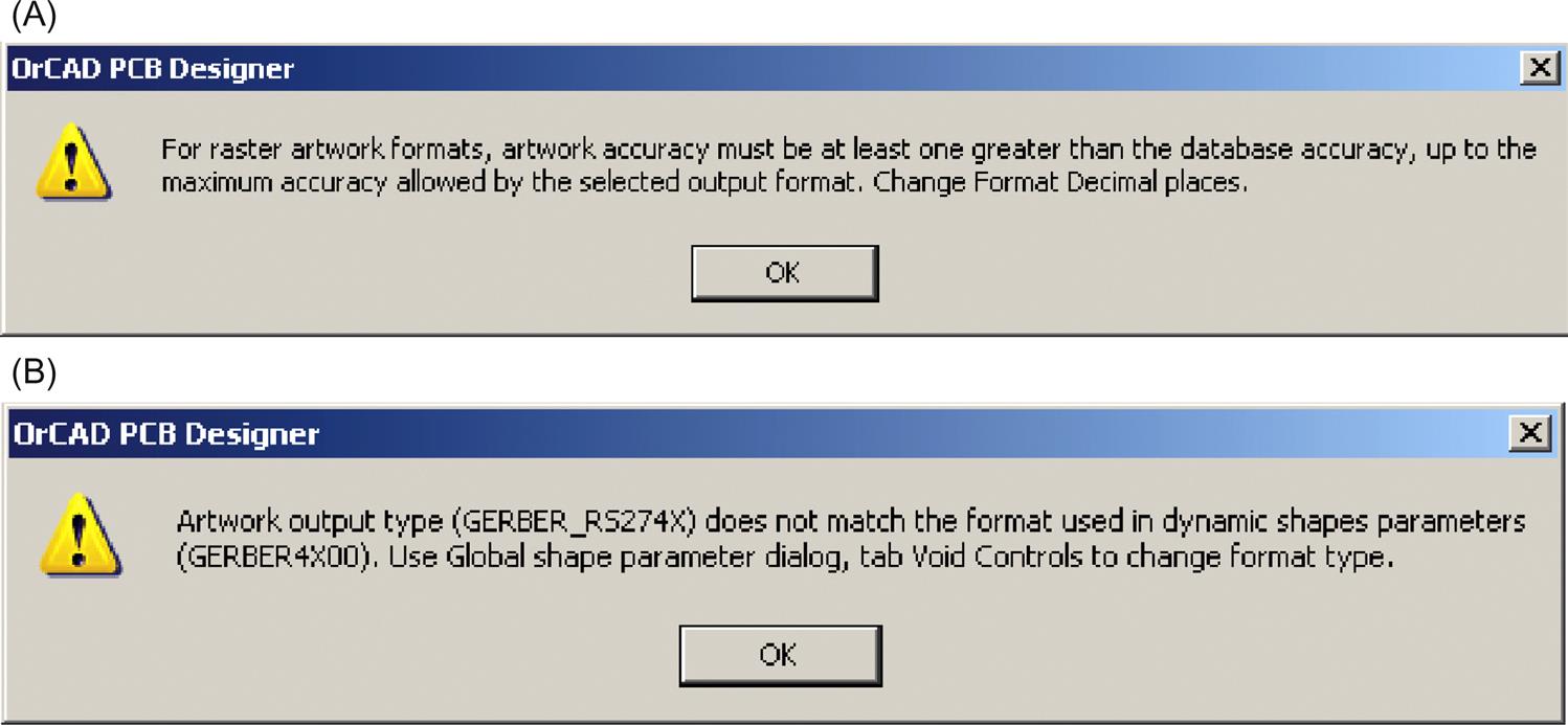
To handle the second warning in Fig. 10.9, change the Artwork Format in the Design Parameter Editor to match the Device type in the Artwork Control Form (Fig. 10.8). To do this, select Setup → Design Parameters… from the menu. At the Design Parameter Editor dialog box, select the Shapes tab then click the Edit global dynamic shape parameters… button to display the dialog box (see Fig. 10.10). Select the Void controls tab and choose Gerber RS274X from the Artwork format: list. Click OK twice to dismiss both dialog boxes.

Film control
The Film Control tab shown in Fig. 10.11 contains folders that in turn contain subclass items. To see the subclass items, click on the + symbol next to the folder you want to view. Initially the form contains folders related to the layer stack-up only. Folders for the other items (e.g., silk screen and soldermask) must be added.

A folder contains related items. For example, recall that there are several types of silk-screen items [component reference designators (REFDES), component outlines, board geometry text, etc.], which belong to different classes and subclasses. These items are collected and organized in folders, and a single silk-screen Gerber file is made from the collective data in that folder.
The first step then is to take an account of all the types of elements you want manufactured with your board. Table 10.3 shows the conductor type artwork elements that need to be generated; these are autogenerated and already exist in the Artwork Control Form. Table 10.4 lists some of the most common nonconductor elements that can be placed on the board. Solderpaste (Pastemask) class elements can also be generated if you are planning on using pick and place machines to populate your board. Three classes contain pick and place elements, as described in the section Generating Pick and Place files. They are added to the Artwork Control Form the same way the soldermask and silk-screen elements are added, which is described next.
Table 10.3
| Class | Subclass |
|---|---|
| Etch | Any layer in the stack-up |
| Pin | Any layer in the stack-up |
| Via | Any layer in the stack-up |
Table 10.4

For this design the top side of the board needs a soldermask and silk screen, while the bottom side of the board needs only the soldermask. Since there is no silk screen on the bottom, we have no bottom silk-screen folder. So from the table, we have three folders: a top-layer silk-screen folder, which includes the Board Geometry, Ref Des, and Package Geometry classes; a top-layer soldermask folder, which includes the Pin and Via classes; and a bottom-layer soldermask folder, which contains the same classes as the top-layer soldermask (only on the bottom layer).
In addition, we need a Gerber file for the board outline. Other types of Gerber files can be made, but for the time being, these are the only ones we need. We begin by adding the top-layer soldermask folder.
Adding elements to the artwork control form
When you add a folder to the control form, all classes that are visible in the design are added. So we begin by turning off all layers except for the classes and subclasses related to the top-layer soldermask. Use the Color dialog box to control the visibility of the classes. To turn off all the layers at once, click the Off button (Global Visibility:) at the top of the dialog box, then click the Apply button at the bottom.
Next, check the box for the Soldermask_Top subclasses in each of the Package Geometry, Board Geometry, Pin, and Via classes. The Package and Board Geometry classes have nothing on them in this design, but it does not hurt to add them to get in the practice of including them for future designs.
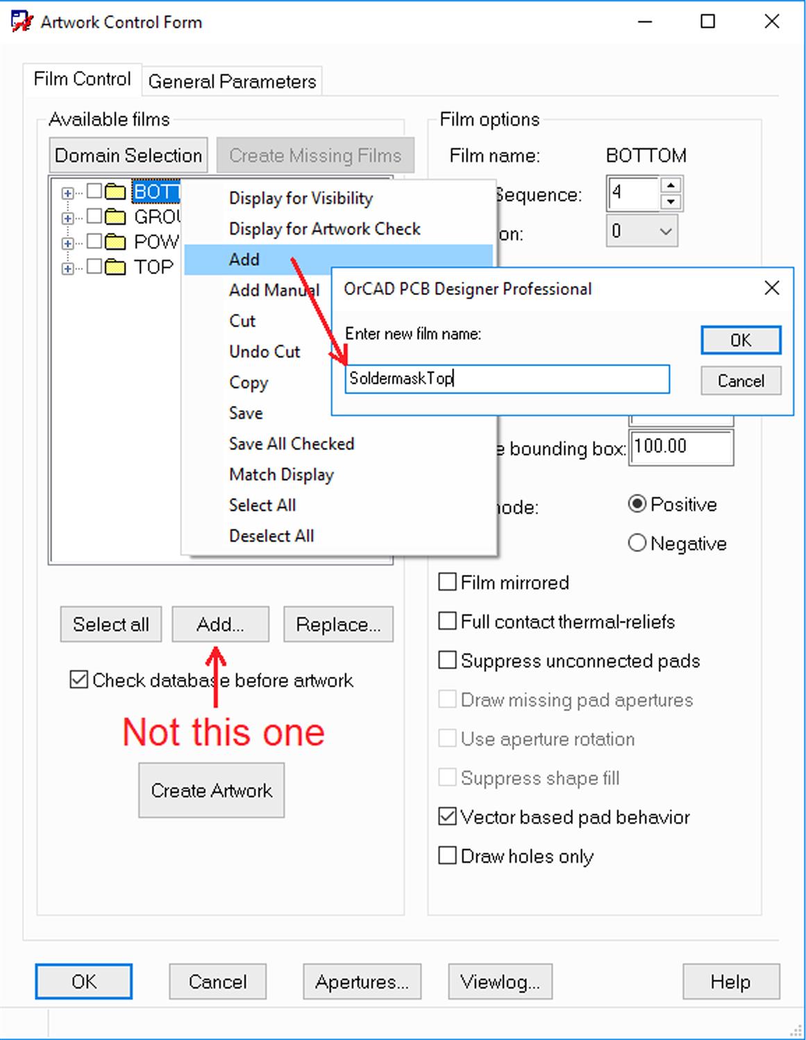
Once these elements are the only ones visible, open the Artwork Control Form. We will add a new folder for the top-layer soldermask items. To add a new folder to the Artwork Control Form, right click on any one of the existing folders and select Add from the pop-up menu (do not use the Add button at the bottom of the form). Enter a name for the folder in the New Film dialog box (see Fig. 10.12). The name does not have to match any PCB Editor class or subclass name, but it can be helpful if it does or is similar. The new folder now will be listed in the form, and it will contain the subclasses visible in the design.
Using this procedure, make a new SoldermaskBottom folder and include the similar classes as the top-layer soldermask folder (VIA, PIN, PACKAGE GEOMETRY, etc.).
Next we add a silk-screen object. As indicated in Table 10.4, many silk-screen objects can be added to the design. You can use the procedure just described to create the silk-screen films too. But there is another way to generate the silk-screen films using the Autosilk tool.
During the part placement steps, it is very possible that silk-screen objects can accidentally be removed (or be unable to be printed) on the soldermask because of openings in the mask, or they can become hidden under components or even printed on top of other silk-screen objects. Keeping the silk-screen objects under control can be a task. Fortunately PCB Editor has a tool that helps us keep track of them, Autosilk.
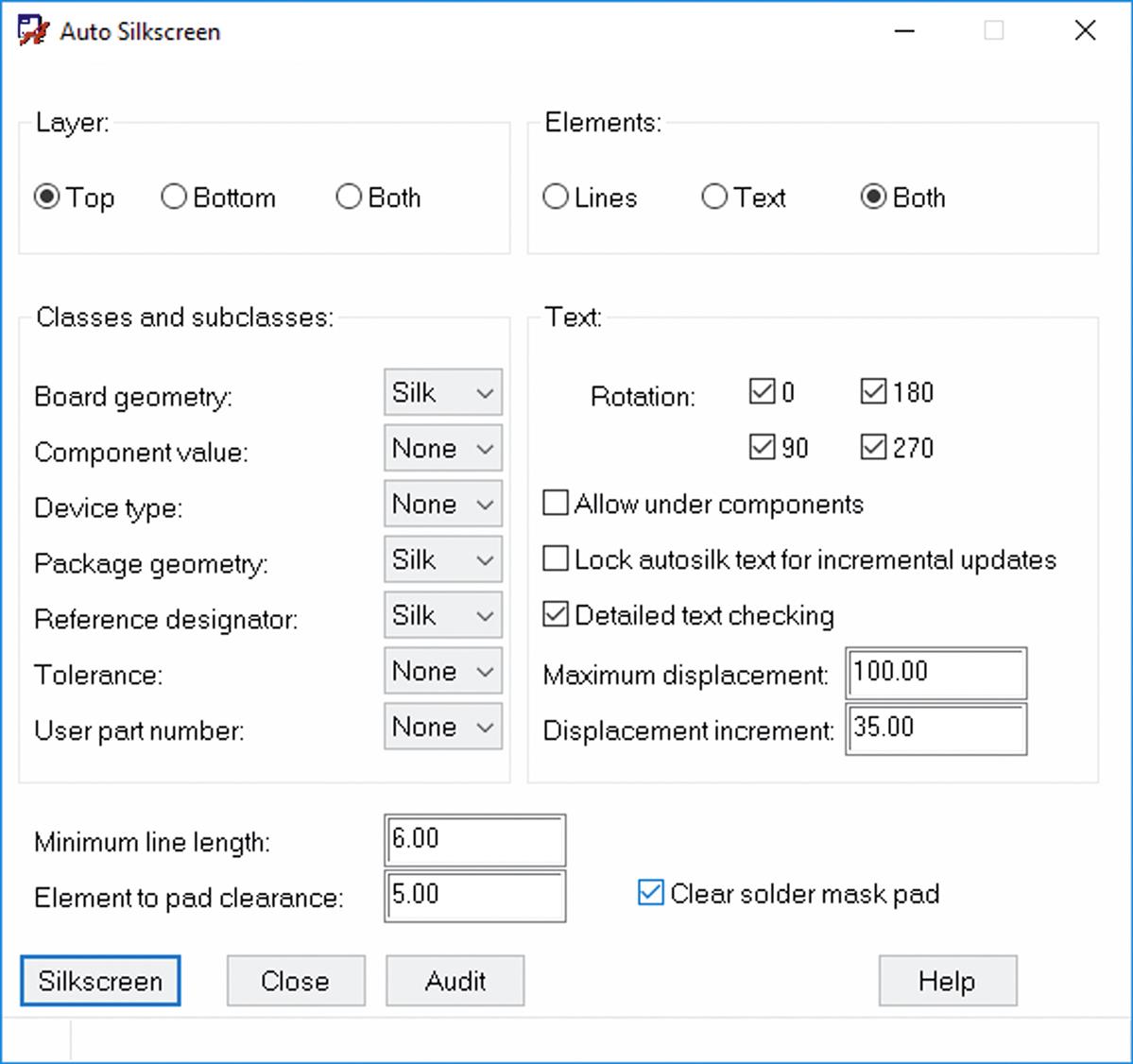
The Autosilk tool takes all of the individual silk-screen elements, combines them into one layer, and makes sure that they are not under components, over padstacks, or too far away from their respective components. To start the Autosilk process, select Manufacture → Silkscreen from the menu bar. At the Auto Silkscreen dialog box (shown in Fig. 10.13), you can select which elements you want added to the common silk-screen files (one for Autosilk_Top and one for Autosilk_Bottom). You can also set default values for some of the physical properties related to silk-screen objects. When the settings are complete, click the Silkscreen button. When the process is complete, the dialog box will dismiss itself and the results will be displayed in the command window. To view the new silk screen, make sure the Manufacturing/Autosilk_Top (or _Bottom) subclass is visible. It is also helpful to make the new silk screen a color different from the other ones.
If you do not notice a big difference, it could be that the new silk screen is directly on top of the original. This will happen if the Autosilk tool does not find anything wrong with the existing ones. To make sure the new silk screen is correct, turn off the original ones (all of them) and look at just the new one, which will be the sum of all the others. Otherwise, you should notice that some of the REFDES were moved away from fan-out vias and outside the place boundary shapes. Depending on how the autorouter routed your board, you may also notice that some of the component outlines are removed where vias are close to the component body. We now add the new silk screen to the artwork form.
If you previously made a silk-screen folder you can add the new autosilk data to the existing folder and remove the other, individual silk-screen elements.
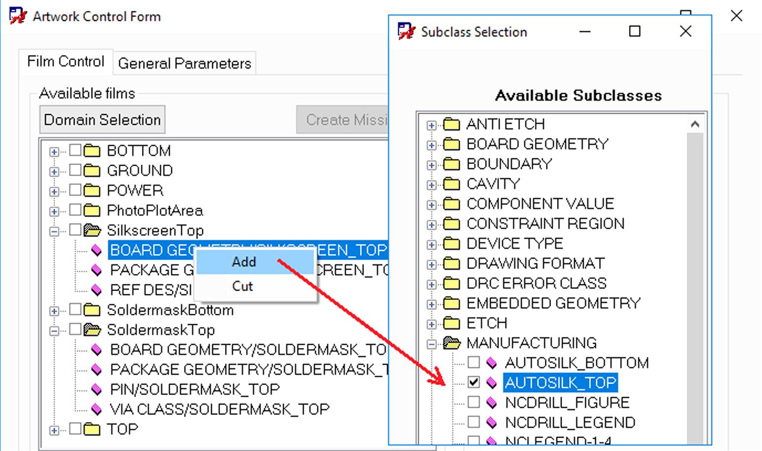
To add an item to an existing folder, right click on any one of the existing items in that folder and select Add from the pop-up menu. At the Subclass Selection dialog box (see Fig. 10.14), check the boxes for the items you want to add and click the OK button. The items will be added to the folder. To delete an item from a film folder, right click on the item and select Cut from the pop-up menu.
The last item to add is the board outline item. The board geometry outline drawn at the beginning of the board design process does not contain Gerber data and is for the designer’s benefit. Gerber data for a board or design outline is contained in the photoplot outline.
Using the previous procedures, add a photoplot outline folder that contains the Manufacturing/Photoplot_Outline class and subclass. An example of the completed artwork list is shown in Fig. 10.15.

We are almost ready to generate the Gerber files. Before we do, check to make sure that the ground and power layers are marked as Negative in the Plot Mode: area of the Artwork Control Form and you have entered a value in the Undefined Line Width: box (a number between 5 and 10 is usually good). If you forget to add a default line-width value, any lines or text that have a width of 0 will be ignored (resulting in large blank areas on the silk screen). And recall from Chapter 8, Making and editing footprints, that many of the silk-screen outlines that come with the library use rectangles instead of lines, and rectangles always have a default width of zero. Also note that if you decide to plot the board outline using the shape created in Design_Outline instead of Photoplot_Outline drawing, you should add Board Geometry/Design_Outline subclass to the PhotoPlotArea folder and set the Undefined line width value to 10 for it as well.
Also, make sure that the Vector based pad behavior option is checked. This applies only to negative planes, but it affects how the unconnected pads on the plane layers will be represented in the artwork. Leaving this option checked removes unused pads from negative planes, which results in a larger (safer) clearance gap.
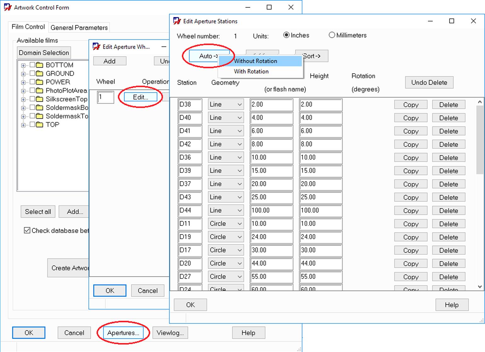
Next, populate the aperture list (skip this step if you’ve selected Gerber RS274X format). Click the Apertures… button (see Fig. 10.16). An Edit Aperture Wheels dialog box will be displayed with at least one entry. Click the Edit button to display the Edit Aperture Stations dialog box. If you do not see a list of entries, click the Auto button and select Without Rotation from the pop-up menu. After the aperture wheel list has been populated, click OK twice to get back to the Artwork Control Form.
To generate the Gerber files, click the Select All button in the Artwork Control Form to check all the folders (or just check the ones you want—the others will not be written or overwritten if they already exist). Then click the Create Artwork button. The command window will report the results and you can read through the photoplot log to look for any errors. Check the working directory and make sure that the files are present. In this example, eight files with the .art extension should have been generated. These are the Gerber files that will be sent to the board manufacturer.
That completes the artwork process. Now we move onto making the drill files.
Generating drill files
Before generating the drill data, it is a good idea to take an inventory of the drill holes. You can do so using the drill legend and the Padstack Definition Report. The report provides all information about each padstack, but the drill legend is much easier to read.
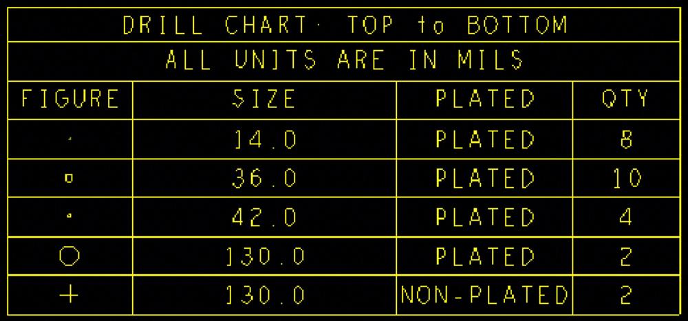
To make a drill legend, zoom out a bit so you have room to place the drill legend. Select Manufacture → Create Drill Table… from the menu. Set the required options in the Drill Legend dialog box, press OK, and the legend will be attached to your pointer. Left click to place it (typically above the board outline or off to one side, but any place is OK). The drill legend (shown in Fig. 10.17) lists the holes by drill figure (specified in the .pad file as designed in Padstack Editor), and it shows the hole sizes, whether the hole is plated or not, and the total quantity of each type of hole. Notice too that, once the drill legend has been generated, the drill symbols are also displayed on each of the padstacks in the design.
Drill file format
As there are different formats for the artwork files, there are several types of drill formats. You need to know the format your board manufacturer requires and apply it to your design. To specify the drill format, select the Ncdrill Param button on the toolbar or select Export → NC Parameters… from the menu to display the NC Parameters dialog box (see Fig. 10.18). At the NC Parameters dialog box, you can enter a header if your manufacturer asks for one, but PCB Editor does not care if you enter one. Enter your board manufacturer’s specifications for the format (e.g., 2.4), zero suppression, Excellon format options, and the like. Once the values are set, click the OK button to save your settings.

The next step is to create the drill file. Select Export → NC Drill… from the menu to display the NC Drill dialog box shown in Fig. 10.19. If you have not scaled your design drawing in any way, enter a scale factor of 1.
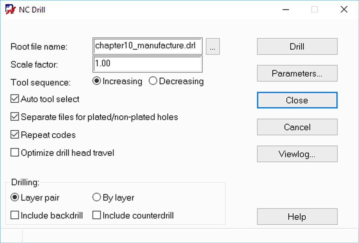
If your board manufacturer prefers a particular tool sequence, you can select that here; otherwise, use the default setting.
Select the Auto tool select option. This option causes PCB Editor to look for a tool list. If one does not exist, it will create one automatically. It also adds drill tool header information to Excellon formatted files. If the Auto tool select option is not enabled, no tool list is created and the drill file contains only drill locations and manual stops where the computer numerical control machine operator is required to indicate the drill tool from a manually generated tool list.
If you know for sure that your board manufacturer can process drill files that contain both plated and nonplated hole information, you can leave the Separate files for plated/non-plated holes option unchecked. Otherwise, check the box to make two distinct drill files. Nonplated hole drill files have np in the filename, as described later, whereas the plated holes do not.
The last two options (repeat codes and optimized head travel) also depend on your board manufacturer’s preferences. If the manufacturer does not specify one way or the other, check them both.
In the Drilling: option box, select the Layer pair option. The By layer option is used for back-drilling and blind/buried-via drilling operations and is explained briefly later.
Click the Drill button to create the drill file(s). For this design with the settings chosen in the NC Drill dialog box, two drill files are generated, chapter10_manufacture-1-4.drl and chapter10_manufacture-1-4-np.drl. The naming convention is filename-startlayer-endlayer.drl. The np in the second file indicates that the file is for the nonplated drill holes. These *.drl files are the NC files your board manufacturer will use during the board fabrication.
If you chose the By layer option in Fig. 10.19, the same files would be generated, but additional drill files would also be generated, where a separate drill file is generated for each layer combination in the stack-up. The drill file names would then be, for a four-layer board for example, filename-bl-1-2.drl, filename-bl-2-3.drl…, filename-bl-3-4.drl, in addition to the one file named filename-1-4.drl. The bl in the file name indicates that the by layer option was checked.
Manually generating a tool list
Instead of using the default nc_tools_auto.txt file, you can specify your own tool list. To do so, you must uncheck the Auto tool select option and create a tool list file, which must have the file name nc_tools.txt. To generate a tool list, open a text editor such as Notepad and save it as nc_tools.txt. A tool list is shown in Fig. 10.20. Each line begins with the diameter of the drill hole. The P or N indicates whether the hole is plated or nonplated. The Tnn is the tool number, and the numbers following that indicate the + and − tolerance. Save the tool list file into the working directory, and PCB Editor will automatically look for it there.

Generating route path files
For most designs and most manufacturers the artwork and drill files provide enough information for them to fabricate your board. But, under certain circumstances, you may also need to generate an NC route path file for the milling operation used to cut your board from a larger panel or for cutting slots or irregularly shaped drill holes in the board.
As described in Chapter 4, Introduction to industry standards, the PCB manufacturers use standard panel sizes to fabricate boards. To help reduce costs, several designs may be placed on a single panel during fabrication and cut apart by a milling machine. The cutting path that the machine takes is called the NC route path. Normally you need not worry about it, since you do not know how the board manufacturer will utilize the panel space. However, if, for example, you want to relay to your manufacturer specific cutting requirements or you buy your boards in panels for mass production pick and place processes and separate the pieces yourself, you need to generate an NC route file.
Generating an NC route file typically requires two steps, but additional steps can be employed, which will be discussed here for completeness. The first required step is to create an ncroutebits.txt tool file and the second is to place an NC route outline. The optional steps are placing cut marks at the board corners and placing cutting path direction indicators on the route path outline.
Establishing an NC route tool list file
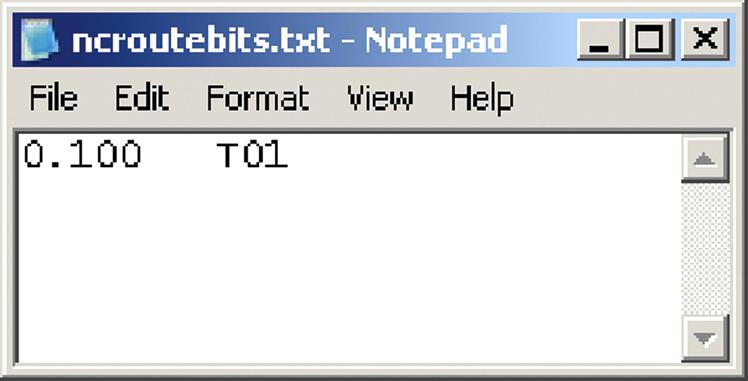
As for the NC drill process, you can automatically create the routing tool list, or you can specify it manually. Setting up an NC route tool list is similar to making the drill tool list described previously. A sample is shown in Fig. 10.21. Use a simple text editor (such as Notepad) and open a blank file. The contents have a line that includes the bit diameter (in inches if your design is using English units or millimeters for metric units) and a tool number for each cutting tool that will be used in the design, as defined by the line widths on the Ncroute_Path subclass. For this example the bit diameter is 0.100 in. (100 mil). Save the file into your working directory with the filename ncroutebits.txt and then close the file.
Cut marks
The actual cutting information is contained in the route path outline described later and not in the cut marks. But we begin with this optional step because cut marks can be used as a guide in placing the route path outline, and it will help make sense of the later steps.
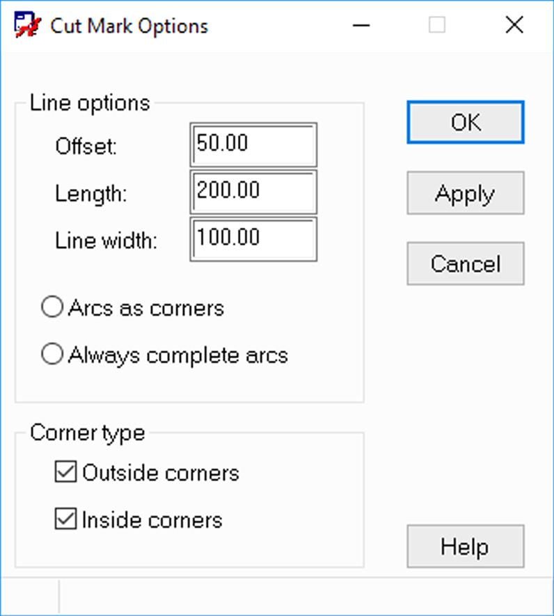
We specified that the bit used to cut around the board is 100 mil in diameter, so the cut marks and the placement of the route outline will be based on that. To place cut marks on your board, select Manufacture → Cut Marks from the menu bar. At the Cut Mark Options dialog box (see Fig. 10.22), enter 100 as the Line width:, because that is the diameter of the cutting bit. Next, assuming that the edge of the bit will cut right along the board edge, the center of the cut path has to be offset by one half of the bit width (50 mil) from the board so that the bit does not cut into the board itself. Therefore enter 50 in the Offset: option. The line length is not critical, as it simply determines the visual length of the mark. A line length of twice the width is a good rule of thumb. If your board is not a simple rectangle, you should select both inside and outside corners in the Corner type box, otherwise the outside only is adequate. When you are ready to place the marks, click the Apply button. PCB Editor automatically places cut marks around the board outline on the Board Geometry/Cut_Marks class and subclass. An example is shown in Fig. 10.23.
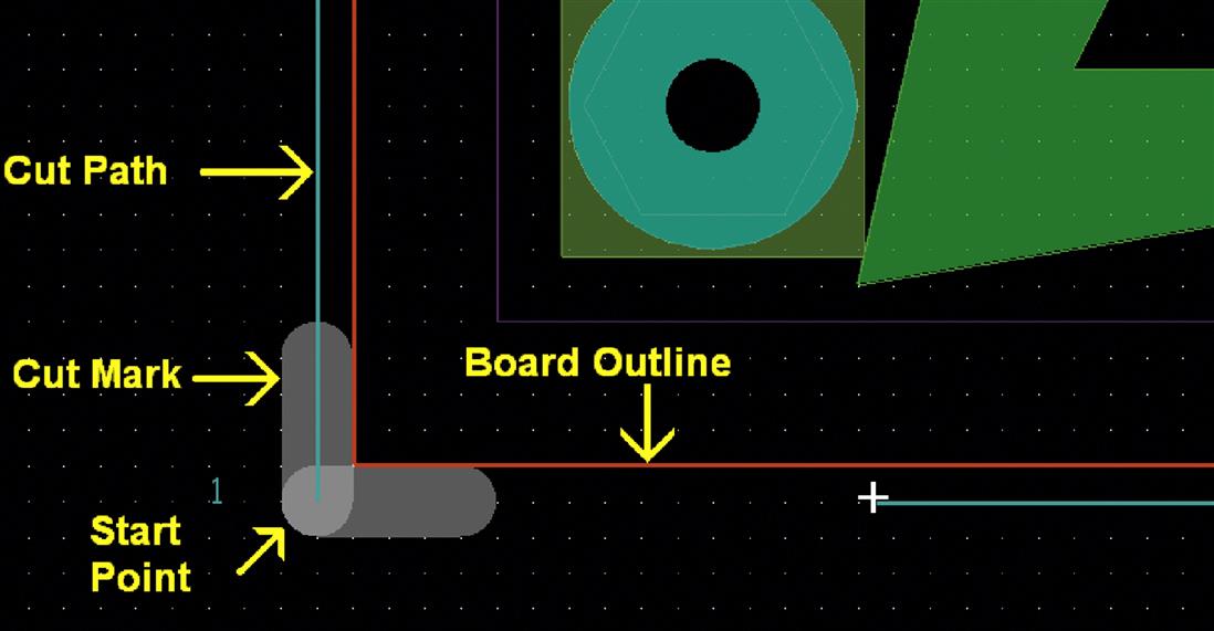
Drawing the cut path
The next step is to place an outline along the cutting path. Begin by selecting the Ncroute_Path subclass under the Board Geometry class in the Options pane. Select the Add Line tool from the toolbar. Set the width of the cut in the Line width: box in the Options pane (100 mil). The center of the cut marks will serve as a drawing guide. Left click and release at the center of the cut mark to begin drawing the cutting path. Continue around the board, drawing the cut path through the center of the cut marks. When you return to the starting point, left click to end the last segment at the starting point and then right click and select Done from the pop-up menu.
Note: You must use the Add Line tool (not a rectangle) to draw the cut path so that you can specify the cut width. PCB Editor uses the width of the line to determine which cutting tool to use from the ncroutebits file when it generates the route file (*.rou). If you have only one cut path (and width) and only one tool in the ncroutebits file, PCB Editor will assume you mean to use that bit for that cut. But if you have multiple cuts (e.g., for edge slots) and multiple bits, then you have to specify the line width and have the correct bits listed in the bit file.
Fig. 10.23 shows a small 1 near the starting point. This is an indicator used to tell the NC machine where to start. A 2 at one of the adjacent corners defines the direction that the cut should be made (not the order the outline was drawn). The numbers are optional, but we will place them as a demonstration.
To place cutting order text objects, select the Add Text tool from the toolbar and the Ncroute_Path subclass under the Board Geometry class in the Options pane (same as for the cutting path outline). Left click near the corner you would like to have the cutting tool start (it does not have to be the corner you started the outline). Enter a 1 in the text block, right click, and select Done from the pop-up menu. That defines the starting point. Use the same procedure to place a 2 at the next corner. The second number defines the direction of the cut path. You can place starting and direction indicators on as many distinct cutting paths as there are on your board. You do not have to place a number at every corner of a closed path unless your board requires a special cutting process.
Generating the route file
The last step in this example is to generate the NC route file. To do so, select Export → NC Route… from the menu. At the NC Route dialog box (see Fig. 10.24), enter a feed rate if you know what it is or leave it blank. You can change the NC Parameters if necessary; we will use the same ones specified during the drill setup. Click the Route button to continue. When the route process is complete, the route log will be displayed. The NC route file will be named boardname.rou.

Verifying the artwork
Before you send your artwork files to the board manufacturer, it is a good idea to review them.
To use PCB Editor to review your artwork files, open a new, blank board design in PCB Editor. To do so select File → New from the PCB Editor menu bar. At the New Drawing dialog box, select Board from the Drawing Type: selection list. Enter a name for the board and choose a destination using the Browse… button then click the OK button. A new, blank design will be opened.
Use the Design tab in the Design Parameter Editor dialog box (Setup → Design Parameters… from the menu) to set up the drawing size needed for the artwork files. Use the Cross Section dialog box (Xsection button on the toolbar) to set up etch layers for each conductor artwork file you intend to import (e.g., top, ground).
Next, select Import → More → Artwork… from the menu (see Fig. 10.25).

At the Load Cadence Artwork dialog box (see Fig. 10.26), select the class and subclass for the artwork you want to import then use the Filename: Browse… button to locate that artwork file. Click the Load file button.

The artwork will be attached to your pointer as an outline with the artwork origin as the insertion point. Click the P button at the bottom of the design window to display the Pick dialog box. Enter 0 0 and click the Pick button. The origin of the artwork file will be placed at the origin of the current drawing.
Fig. 10.27 shows an example of what the top-layer looks like when importing the Top.art file. The traces (clines) are now just lines and no net information is associated with them. The pads are shapes and have a dummy net property attached to them, so DRC markers are placed wherever a line crosses a pad (even if it is not supposed to). Since we are just reviewing the artwork, you can disable the DRC markers by turning off that layer in the Color Dialog panel (go to the Stack-Up folder and disable the entire DRC column). Alternatively you can set up layer subclasses in the manufacturing class and import the files there, where the DRC checker will ignore them.
When you import a negative plane layer, it is displayed as an actual negative image, not the way PCB Editor displays it when you are in the design mode. In the negative view, what you see is what will be removed during the etch process.
When you import the silk-screen file, you can import it into the Board Geometry class or into the Manufacturing class, but if you created the silkscreen using the autosilk feature, it is best to import it into the Manufacturing class.
The types of artwork files that you can import are limited to the basic etch and nonetch objects. You cannot import machining information (e.g., drilling and milling) or photoplot information. If you want to review that information, you need to use a computer-aided manufacturing (CAM) tool.
Using CAD tools to 3D model the printed circuit board design
Before you send the Gerber files off to the board house to be manufactured, you might want to know if the board will be physically compatible with the house mounting hardware and enclosure (i.e., will it fit?). You can export the design information from PCB Editor to a .DXF file, which you can open with most popular CAD drawing packages.
Sincerely speaking the design has a tremendous amount of information, a lot of which does not need to be exported to a drawing file. To select layers to plot, use the Colors Dialog panel to turn on only the layers you want to include in the drawing.
To export a PCB design as a .DXF file, select Export → MCAD → DXF… from the menu. At the DXF Out dialog box (Fig. 10.28), enter a name in the file name box. Click the Layer conversion file entry Browse… button. At the dialog box, click the Open button to accept the default file name or enter a new name and then click Open.
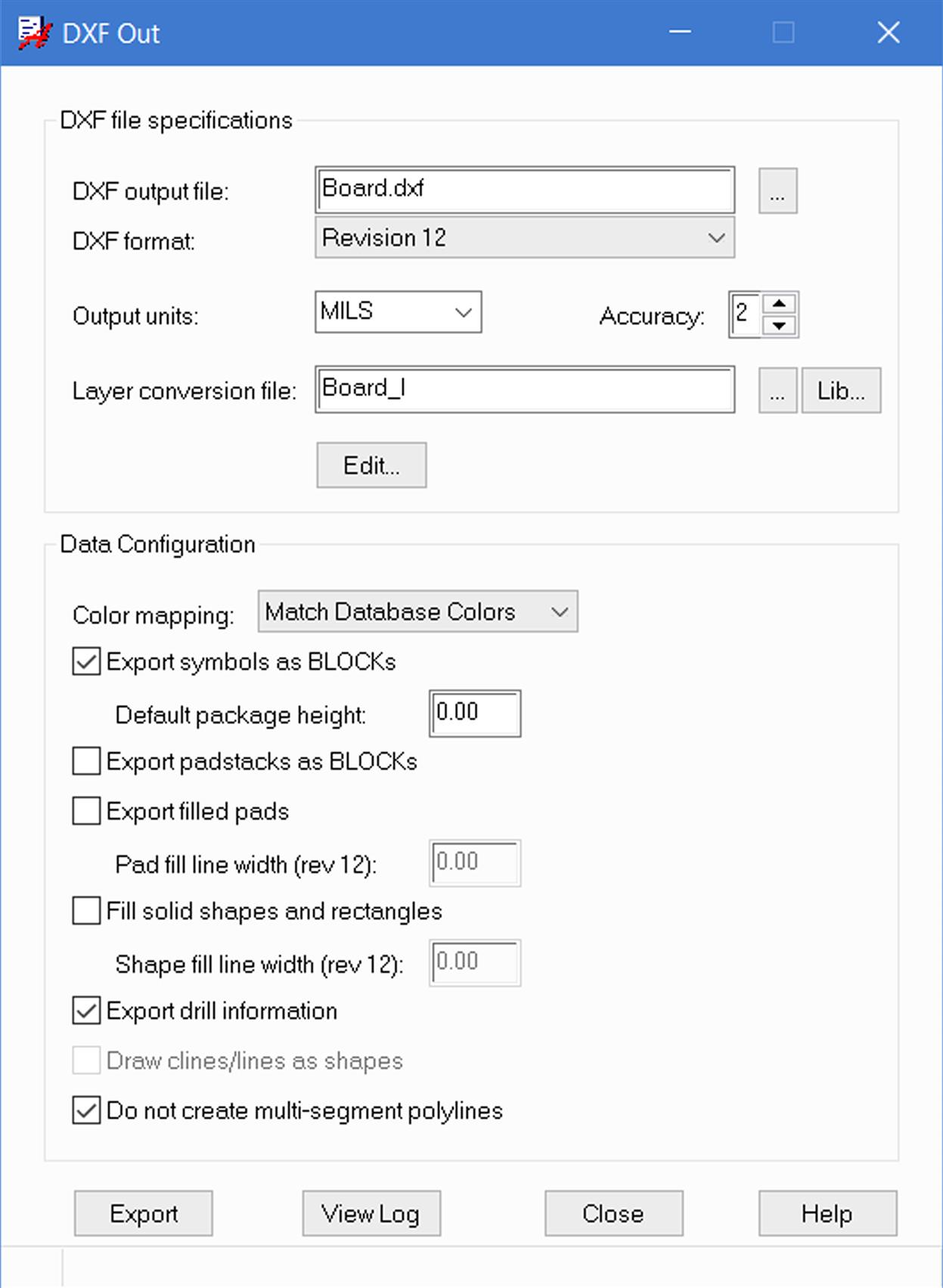
The conversion file needs to be set up. To do so, click the Edit button to display the conversion file editing dialog box shown in Fig. 10.29. You can specify layers and names or map the PCB Editor classes directly to the new DXF layers. The options shown in the figure map them directly. To execute the conversion, click the Map button. The class and subclass names will be combined into one name in the DXF layer boxes. Click OK to dismiss the conversion dialog box and return to the DXF Out dialog box.

In the Data Configuration section, you can leave everything unchecked, but the objects in the DXF file will be of two dimensional. If you want a 3D representation, then at a minimum you need to check the Export symbols and padstacks as BLOCKS option. If you also check the Fill options, flat objects (traces and silk screens) will be filled in instead of just an outline. This will make the DXF drawing look richer, but it significantly increases the memory usage and drawing regeneration time.
Once the remaining options are set in the DXF Out dialog box, click the Export button.
When the conversion is complete, the DXF file can be opened with a CAD program.
Fig. 10.30 shows a 3D model of the design using a popular drawing program (the colors were modified with the CAD program). The CAD program can then be used to add the enclosure and mounting hardware to verify form, fit, and function. Dimensions and other manufacturing information can easily be added to the drawing file to fully describe manufacturing and assembly instructions.
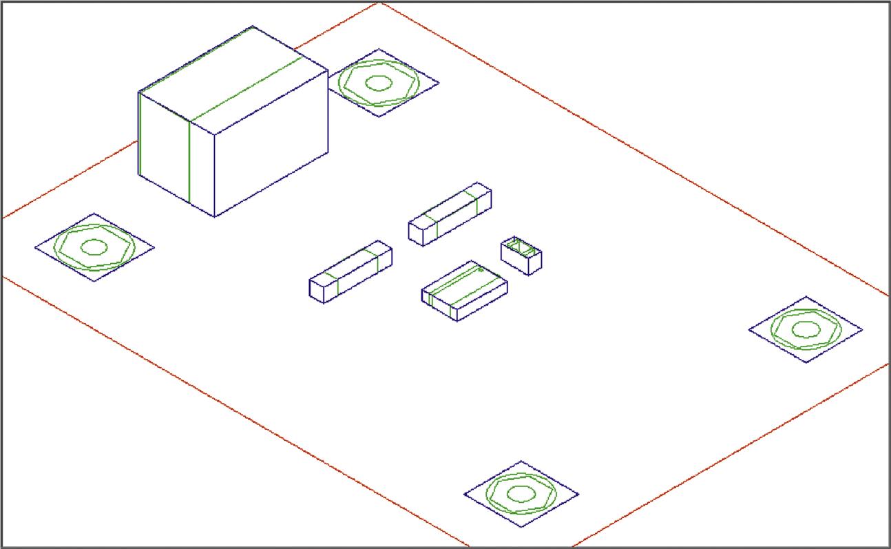
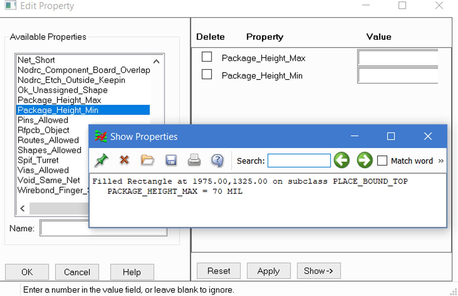
The height information that the CAD program uses is derived from the PACKAGE_HEIGHT_MAX property of the component’s place-bound outline in PCB Editor. You can view the property by selecting Edit → Object Properties… from the menu and left clicking on the component. The information shown in Fig. 10.31 is from the place boundary outline of J1. As mentioned earlier, place boundaries can be drawn using filled rectangles or shapes. In some CAD programs, filled rectangles behave as solid objects whereas shapes behave as wire frame objects.
There are other options to export the information to CAD program. You can export IDF, IDX, or STEP model of your project. You can also view the 3D image in the PCB Editor using Display → 3D Canvas. Press Shift + Mouse Wheel and drag the mouse to rotate the view. In order to see the more realistic image you can attach the 3D STEP model to each component pattern using Setup → Step Mapping dialog box. Various STEP models are available from the component manufacturer websites or from the 3D component collection portals such as www.ultralibrarian.com where you can find the model by its part number. It’s recommended that the component STEP models are changed in the MCAD program so that its orientation and origin were the same as for the PCB footprint in your design. This will simplify the mapping procedure as well as improve the ECAD–MCAD collaboration process.
Fabricating the board
Not all board houses are the same. While most follow certain fabrication standards, not all have the same fabrication capabilities (e.g., number of layers, copper thickness, and drill sizes). There are also differences in design submission policies and minimum order and billing practices.
Many board houses use an online file submission and quote process, but not all do. Some have you send the Gerber files by e-mail, and after someone looks at them with CAM software (such as GerbTool or CAM350), the company sends you a quote via e-mail.
An example of the generated Gerber files that would be sent to the board manufacturer is shown in Fig. 10.32.

Fabricated PCB inspection and testing
Regardless of which house fabricates your boards, you should perform an inspection of the boards, especially if it is a first run. You may also want to do some initial electrical tests (continuity and isolation), especially on the power and ground, before you place any components on the board. IPC-2515A and IPC-6011 outline many types of inspection and acceptance tests.
The next step is to populate the boards. The next section describes how to generate a file describing your board and parts that pick and place machines can use to populate the board.
Generating pick and place files
There are many types of pick and place machines, each with its own programming and setup requirements. As an example here, we just look at the basics most machines require. At a minimum the machine needs to know which parts are to be placed, where they are to be placed, and in what rotation. When placing large quantities of parts on a board, it is also often necessary to include part numbers, as there may be more than one type of component with the same value. For example, the only way to differentiate between a size 1206 smd, 0.1%, 1k resistor and a size 1206 smd, 1%, 1k resistor is by the part numbers. So we will customize the pick and place list to include the components’ part numbers so that the assembler will know which part to place in which tray on the machine and how to program it.
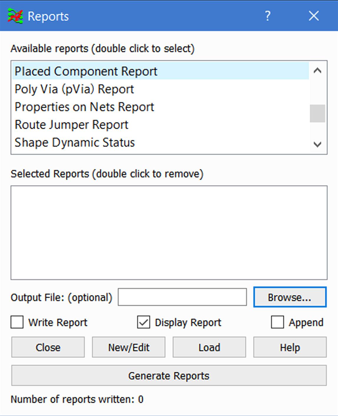
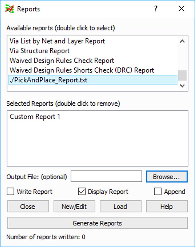
The pick and place part list is a report. In general you generate reports by selecting Export → Reports from the menu or the Reports button on the toolbar if it is displayed. The Reports dialog box is shown in Fig. 10.33. There is no specific report for pick and place machines, but the Placed Component Report comes close, so we begin with that.
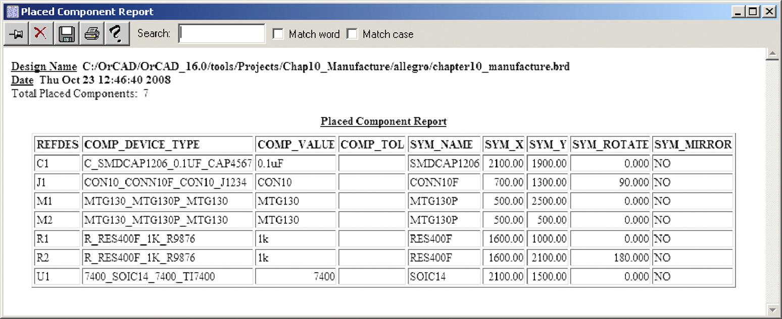
The default Placed Component Report is shown in Fig. 10.34. This report provides the REFDES, the symbol X and Y coordinates, and the rotation, but no part numbers, and it contains other information that we do not care about.
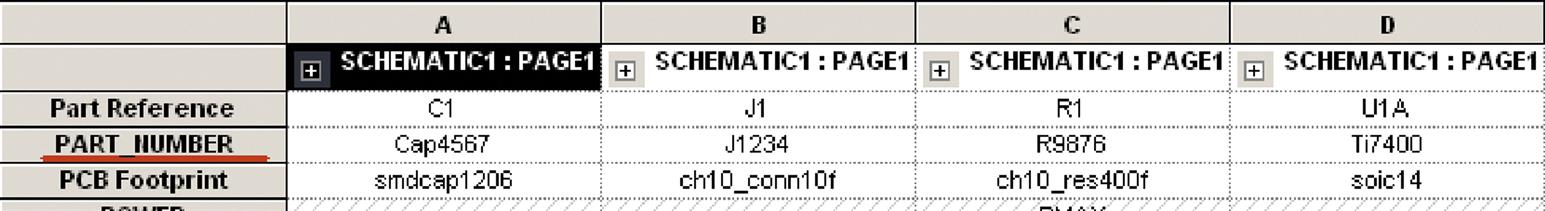
We can create a report that will provide the part number, but this information must already be assigned to each part. An easy way to do that is to add the part number to the part in Capture. To add a part number to a component, select the component (or components) on the schematic, right click and select Edit Properties… from the pop-up menu. Enter the part numbers in the PART_NUMBER cells in the spreadsheet, as shown in Fig. 10.35. Perform an engineering change order to update the part number information to the board design in PCB Editor (if it has not already been done).
Make sure that the parts have the part number property attached to them. To check, select the Show Element tool from the toolbar and select one of the parts. The PART_NUMBER property should be visible in the Show Element text box that pops up.
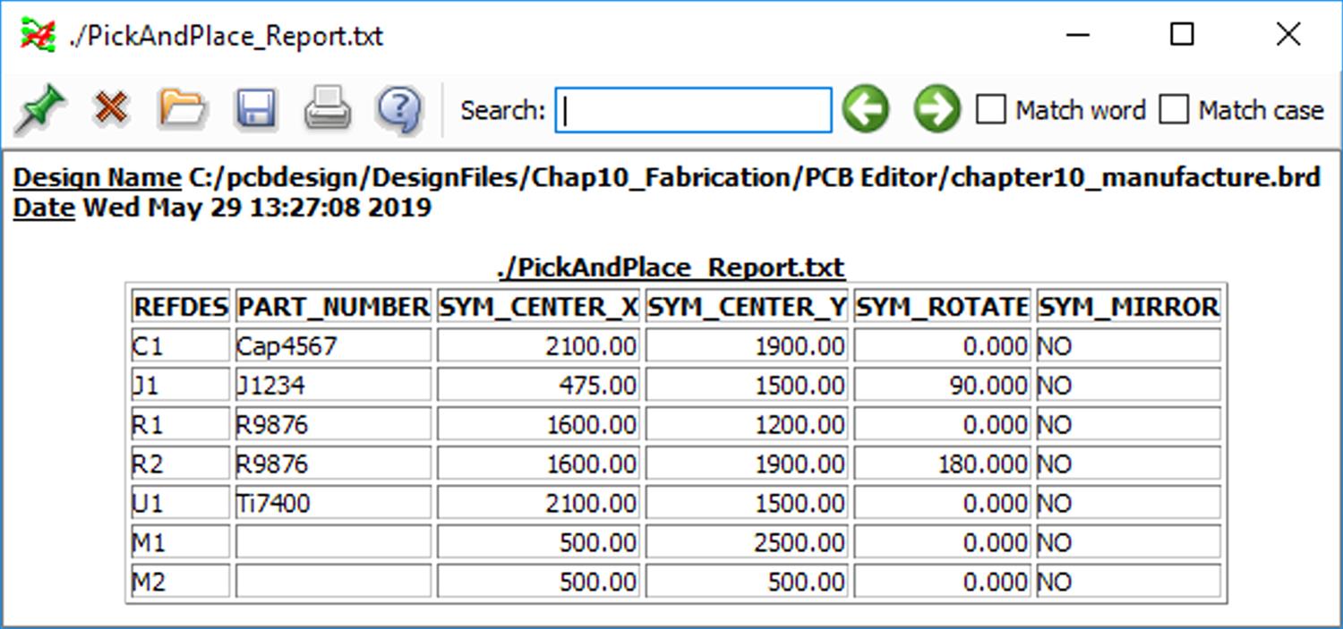
The next step is to create a custom report. To make a new report, display the Reports dialog box (see Fig. 10.33). Click the New/Edit button at the bottom. At the Extract UI dialog box (see Fig. 10.36), select the Data Fields tab, select COMPONENT from the database list, and double-click REFDES in the Available Fields list to add it to the Current Configuration window. Next, select the Properties tab, scroll down the Available Properties window until you find PART_NUMBER, then double-click it to add it to the list. Return to the Data Fields tab and look for SYM_CENTER_X and SYM_CENTER_Y and add them to the list. Also add SYM_ROTATE to the list. You may also add the SYM_MIRROR to the list, to show the component's side for 2-sided SMT assembly.

The final list is shown in Fig. 10.36. The order that the properties are listed in the dialog box is the order that they will appear in the report. If you need change the order, use the up and down arrows to the right of the list to move a selected item.
To save this report, click the Save button and enter a name in the dialog box that pops up. Click the OK button to dismiss the Extract UI dialog box.
To generate the new report, scroll all the way down to the bottom of the Available Reports list in the Reports dialog box (Fig. 10.37), and your report will be listed.
Double click the new report to select it then click the Generate Reports button. The report is shown in Fig. 10.38. You can save the report as an html file or select and copy the data from the report and paste it into a text or Excel file, which the pick and place machine programmer can use to set up the machine to populate your board.