Defining the Layer Stack-Up for Split planes
As discussed in the first example, it is a good idea to have the board constraints defined prior to starting the board layout. Items to consider are the board technology, board size constraints, noise and shielding requirements, part placement restrictions, the number of Power and Ground planes and Signal layers, and trace width and spacing requirements.
The voltage and current constraints are similar to those of the analog design, except that the analog parts should be segregated from the digital parts on the board. In the first analog design example, we used four planes for V+, V−, and ground. A similar approach could be taken here, but in this example we use one plane for V+, V−, and VCC, and one plane for both the analog and the digital grounds, as shown in
Figure 9-94
, to demonstrate the process of working with split planes. The default PWR layer is divided into three completely separate Power-plane areas, using three copper shapes to supply analog V+ (PA+), analog V− (PA−), and digital VCC (PD), as indicated in the figure. The Ground plane is partially divided into two Ground planes for analog ground (AGND) and digital ground (GND) but left connected by a small section of copper near the connector’s ground pin. This arrangement segregates the analog components from the digital components and therefore reduces switching noise in the analog circuitry. To accomplish this, the board requires two Plane layers and at least two Routing layers.
Table 9-5
lists the design constraints.
 |
| Figure 9-94 A mixed-signal power and ground system. |
To begin the board layout, we follow the same procedure as outlined at the beginning of these examples and discussed in detail in the analog design example.
From Capture, perform the Create Netlist procedure and launch PCB Editor.
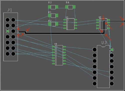
As described in the first example, draw the board outline, use one of the place tools to find and place parts into the board outline, and perform a DRC to check for footprint problems prior to doing anything else.
Figure 9-95
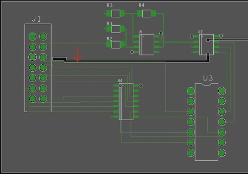
shows an example of how the parts might be placed. Notice that the analog parts are segregated from the digital parts.
 |
| Figure 9-95 Initial parts placement for the mixed analog and digital design. |
When the board constraints were defined earlier, we said that we wanted two Plane layers and two Routing layers, so we need to add the Plane layers. Follow the procedure from the first example (right click and add layers) and add the two plane layers, as shown in
Figure 9-96
.
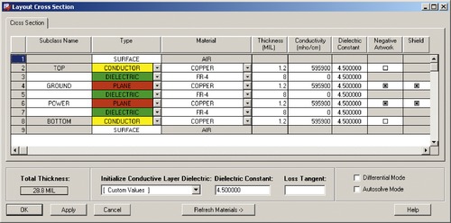 |
| Figure 9-96 Layer stack-up for the mixed-signal board design. |
SETTING UP A SPLIT GND PLANE
The objective in splitting a Plane layer into analog and digital sections is to remove copper from the plane using a shape void.
Figure 9-97
shows the desired split Ground plane. Electrically the AGND and GND nets are the same but physically we want to separate them. To do this, a copper shape, which is attached to the GND net, is added to the Ground layer. This makes them electrically connected. To physically separate the analog from digital circuitry, we create a void strip between the analog and digital areas of the board.
 |
| Figure 9-97 A split place for analog and digital circuits. |
Before placing the plane, you may need to adjust your route grid. Set it to about 5
mils, because you need the resolution to properly place the vertices (corners).
To add the GND shape to the ground plane, use the procedure used in the first example. In short, select
Setup → Outlines → Plane Outline… from the menu bar (or use the Shape Add tool and select
Dynamic copper in the
Options pane). Select the
Ground plane, the
GND net, and the
Draw Rectangle option in the
Place Outline dialog box. Draw the Ground plane then click
OK to dismiss the dialog box. To view the thermal reliefs, follow the procedure used in the first example (
View thermal pads in the
Design Parameters dialog box and assign flashes to the padstacks as necessary). Next we split the plane into analog and digital areas.
Note: Ground planes can be drawn with filled rectangles, static shapes, or dynamic copper shapes. For best results use dynamic copper shapes. To identify the shape type of existing shapes, hover your mouse over the shape edge (make sure the
Shapes option is selected in the
Find filter pane). To change a shape to dynamic copper, select
Shape → Change Shape Type from the menu then left click the shape you want to change.
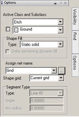
To split a plane, select the plane layer from the
Options tab by selecting the
Etch class and
Ground subclass. Select the
Shape Void Polygon button,
 , on the toolbar. At the command prompt, PCB Editor asks
Pick shape or void to edit. Left click the GND plane. PCB Editor then asks
Pick void coordinates. Left click at the vertices of the void area you want to define, as shown by the arrows in
Figure 9-97
. Draw the void so that the analog and digital areas are separate but leave a connected area by the connector, J1, so that the two Ground planes remain electrically connected. The void between the ground areas should be about 50
mils wide.
, on the toolbar. At the command prompt, PCB Editor asks
Pick shape or void to edit. Left click the GND plane. PCB Editor then asks
Pick void coordinates. Left click at the vertices of the void area you want to define, as shown by the arrows in
Figure 9-97
. Draw the void so that the analog and digital areas are separate but leave a connected area by the connector, J1, so that the two Ground planes remain electrically connected. The void between the ground areas should be about 50
mils wide.
| Shape Void Polygon button
|
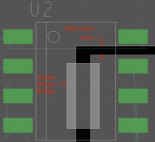
U2 is the analog-to-digital converter (ADC) and has both analog and digital properties. Some ADC manufacturers specify that the analog and digital grounds should be common near the IC. Right now the analog and digital grounds are separate, but we will connect them directly under the IC by placing a small patch of copper, which will be connected to the GND net, to bridge the void separating the analog and digital planes, then merge the patch with the main Ground plane.
To create a copper bridge, select the
Shape Add Rectangle button,
 , and use the
Options tab to define the shape on the Etch Ground plane and connect it to the GND net, as shown in
Figure 9-98
. Note that, if the Ground plane was made with a dynamic copper shape, then the bridge also needs to be dynamic copper rather than static filled.
, and use the
Options tab to define the shape on the Etch Ground plane and connect it to the GND net, as shown in
Figure 9-98
. Note that, if the Ground plane was made with a dynamic copper shape, then the bridge also needs to be dynamic copper rather than static filled.
| Shape Add Rectangle button
|
 |
| Figure 9-98 Setting the properties of the copper bridge. |
Place the bridge as shown in
Figure 9-99
. Left click and release at the upper left and lower right corners to draw the shape. Make sure to overlap the shape and the Ground plane to allow the merge process to work properly.
 |
| Figure 9-99 Placing a copper shape to bridge the two ground planes. |
To merge copper shapes, select
Shape → Merge Shapes from the menu bar. At the command line, PCB Editor will ask you to
Pick primary shape to merge to. Select the Ground plane. Then PCB Editor will ask
Pick shapes to be merged. Select the bridge, right click, and select
Done from the pop-up menu. The bridge is now part of the Ground plane.
Notice that at the J1 connector we have the “common ground area” in
Figure 9-97
, but that the analog and digital ground areas are separated throughout the rest of the board. The area under the ADC does not defeat the “split” plane. Recall from
Chapter 6
that return currents follow the path of least impedance, so return currents related to U3 and U4 do not go out of their way to pass through the area under the ADC.
Unlike the ground system, in which there is really only one ground net and one Ground plane, the power system has three distinct power nets (V+, V−, and VCC) that need to share the Power plane. To accomplish this, distinct copper areas are drawn for each net on the one Power plane. The goal is shown in
Figure 9-100
.
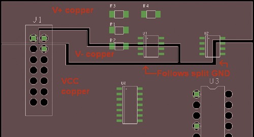 |
| Figure 9-100 Setting up multiple power areas on a single plane. |
We begin by placing the VCC Power plane in the digital section of the board. As described in previous sections, we start by selecting
Setup → Outlines → Plane Outline from the menu bar. At the
Place Outline dialog box, select the Power plane and select the VCC net. Select
Draw Polygon and left click to place the eight vertices that make up the VCC plane area. Click
OK to complete the process and close the dialog box. Keep the VCC plane above the digital Ground plane and away from the void area. Once you have the VCC plane area drawn, there should be a thermal relief around the connector pin attached to VCC (pin 4 in this example).
Repeat this process for the V+ and V− plane areas. Note that the area between the digital and analog plane areas should match up with the void that was placed in the GND plane until you get close to the connector. Also note that we need not place voids on the Plane layer to split the plane, since the copper areas are distinct objects and do not need to be split. When drawing the V+ copper pour, make sure to include J1 pin 1 and the V+ fan-outs for U1 pin 7 and U2 pin 8 and make sure the copper pour stays on the analog side of the split Ground plane. When drawing the V− copper pour, make sure to include J1 pin 2 within the boundary and stay on the analog side of the Ground plane, as shown in
Figure 9-100
.
Setting Up Routing Constraints
Before fanning out or routing the board, we need to set up the design constraints using the Constraint Manager. Launch the Constraint Manager by selecting the
Cmgr button,
 , on the toolbar.
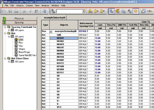
To change the spacing constraint, select the
Spacing tab and the
Line icon under the
Net folder. Change some of the nets to whatever you like, just to see what happens.
Figure 9-101
shows the line-to-line spacing of all the nonbus nets set to 15
mils.
, on the toolbar.
To change the spacing constraint, select the
Spacing tab and the
Line icon under the
Net folder. Change some of the nets to whatever you like, just to see what happens.
Figure 9-101
shows the line-to-line spacing of all the nonbus nets set to 15
mils.
| Cmgr button
|
 |
| Figure 9-101 Setting the trace spacing rules. |
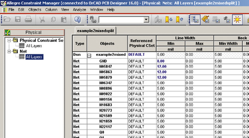
To change the line width constraint, select the
Physical tab and the
All Layers icon under the
Net folder. Change a couple of the minimum line widths to see the effect. The GND and a couple of the analog nets were changed, as shown in
Figure 9-102
. Note that changing the GND line thickness changes the width of the fan-out traces (the short trace going from an SMD pad to the via to GND) and thermal spokes on positive Plane layers, as we will see.
 |
| Figure 9-102 Setting the trace width rules. |
Next we begin the process of fanning out power and ground. We could disable all the nets except for the power and ground nets to do the fan-out, as we did in the last example, but we will force the autorouter to ignore the signal nets, so that we need not do that extra step. Perform the fan-out as described in the first couple of steps of the first example. Select
Route → Route Automatic…from the menu. In the
Automatic Router dialog box, select the
Router Setup tab and select
Specify routing passes in the
Strategy section. Select the
Routing Passes tab, select
Fanout option, and deselect the
Route and
Clean options. Click the
Params… button. In the
SPECCTRA Automatic Router Parameters dialog box, select only the
Power Nets option under the
Pin Types section. Click
OK then click
Route to generate the fan-outs.
Check the fan-outs to make sure the router did its job and check that there are no DRC errors by checking the
Status dialog box (
Display → Status…) or generating a DRC report (
Tools menu). If everything looks OK, then we can route the rest of the board.
To make sure that the fan-outs or any manually routed traces remain intact, they should be locked in place (fixed). To fix traces, display the Constraint Manager and select the
Properties tab. Under the
Net folder, select the
General Properties icon. Set the
On flag in the
Fixed column for any trace you want to protect. Alternately you can use the
Fix button,
 , and the
Unfix button,
, and the
Unfix button,
 , on the toolbar to select traces and components to fix or unfix.
| Fix button
|
| Unfix button
|
After performing the fan-out and fixing routed traces to protect them, we can
set up to route the signal nets. Select
Route → Route Automatic… from the menu. In the
Automatic Router dialog box, select the
Router Setup tab and select
Specify routing passes in the
Strategy section. Select the
Routing Passes tab and select the
Route and
Clean options and deselect the
Fanout option; click the
Route button to route the rest of the board. If you want to restrict which signal nets get routed, use the Constraint Manager to set routing constraints. Use the
Route Restrictions on the
Properties tab of the Constraint Manager.
An example of a routed board is shown in
Figure 9-103
.
 |
| Figure 9-103 The circuit after fan-out and routing. |
As in the earlier example, a postrouting inspection is performed after autorouting to look for problem areas, and offending traces are unrouted then rerouted.
Figure 9-103
shows an area that could use some work (
Figure 9-104
shows a close up view of the area). The red arrow points to a trace that was routed over the void in the GND plane.
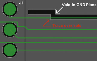 |
| Figure 9-104 Look for problem areas after autorouting. |
As described in
Chapter 6
, we do not want this to occur, as it increases the loop inductance of the trace (an impedance-matching issue), which can lead to ringing problems and EMI. In this case the easiest fix is to simply move the trace down.
To move a trace, select the Slide tool,
 , left click and release on the trace to select it. Move the mouse to the desired location, left click and release to place the trace. To prevent this from happening on subsequent routing actions, we can also place a Route Keep-out area in the void to keep the autorouter from routing other traces over the void.
| Slide tool
|
ADDING ROUTE KEEP-OUT AREAS
To place a route keep-out shape area, select the
Route Keepout class and
Top subclass from the
Options tab. Select the Shape Add tool and place a polygon on the top layer that overlaps the void by 10 to 20
mils, as shown in
Figure 9-105
. This will keep traces away from the void.
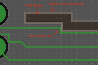 |
| Figure 9-105 Add a route keep-out shape to control routing. |
Another potential problem area is the traces that run between the microcontroller (U3) and the ADC (U2). The traces run side by side in close proximity for a relatively long distance. The traces should be moved farther apart (use the Slide tool as described previously) or guard traces can be added to provide isolation between the traces (discussed later and in the next example). The traces that run from U4 to J1 could also be a problem. A simple solution there would be to move some of the traces to the bottom layer, as described next.
MOVING A ROUTED TRACE TO A DIFFERENT LAYER
As long as a trace has a through hole or via on each of its ends, you can easily change which layer the trace is on without having to rip it up.
To move a routed trace to another layer, select the
General Edit button,
 , select the trace you want to move (use the
Find filter if necessary), right click, and select
Change to layer from the pop-up menu then select the layer to which you want the trace to move, as shown in
Figure 9-106
.
, select the trace you want to move (use the
Find filter if necessary), right click, and select
Change to layer from the pop-up menu then select the layer to which you want the trace to move, as shown in
Figure 9-106
.
| General edit Button
|
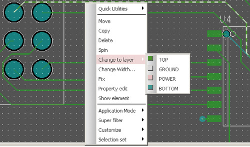 |
| Figure 9-106 Moving a trace to a different layer. |
ADDING GROUND PLANES AND GUARD TRACES TO ROUTING LAYERS
As discussed at the beginning of these examples and in
Chapter 6
, you can reduce noise levels on signal lines by surrounding traces with copper planes and guard traces. Not everyone agrees with this practice, but it is demonstrated here in the interest of completeness. The following procedures demonstrate how to use the Add Connect tool to add ground nets and use shapes to add copper planes to routing layers.
ROUTING GUARD TRACES AND RINGS
If you have one or two traces that could have cross-talk problems, you can add guard traces between them that can be attached to the Ground plane with vias. You can also add guard rings around component pins. Like the guard traces, the guard rings are attached to the Ground plane with vias. It should be noted though that their usefulness is debated in the literature, because they can cause more problems than they fix if not applied correctly (see Appendix E for references).
Figure 9-107
shows examples of guard traces between the control and the data lines and guard rings around one of the microcontroller pins.
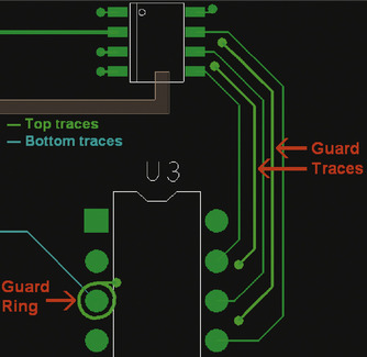 |
| Figure 9-107 Add guard traces to help minimize cross talk. |
To place guard traces that are attached to the Ground plane, select the Ground plane on the
Options tab and select the Add Connect tool. Left click on the Ground plane where you want to begin the guard trace. Right click and select
Add Via from the pop-up menu. The Add Connect tool should still be active and you should now be on the Top layer (but check the
Options tab to make sure). Draw the trace where you want the guards to be. At the end of the trace, right click and select
Add Via. At various intervals along the trace, add vias to securely stitch the guard trace to the ground plane. To add the vias, select the Add Connect tool, left click on the trace where you want the via, right click and select
Add Via. Repeat this where ever a via is needed.
To add a guard ring around a component pin that is attached to the Ground plane, start by placing a via attached to the Ground plane near where the guard ring will be. The via is used to start and end the ring and can be moved to a different location after the ring is made. To begin with, the via should be placed across from (or above) one of the vertical (or horizontal) quadrant points, indicated by the numbered squares in
Figure 9-108
. To route a guard ring as shown in the figure, select the Ground plane from the
Options tab, select the
Add Connect tool and left click at the square marked
1, and immediately right click and select
Add Via. Check the
Options tab to make sure you are on the layer you want the ring to be, then left click at the
2 position. Right click and navigate through the pop-up menu to
Options → Line Types → Arc, or select the
Arc option on the
Options tab. Route a curved trace around the pin and left click at point
3 continuing to points
4 and
5. At point
6, left click to tack the trace then right click and select
Done from the pop-up menu. Once the ring is in place, you can use the Slide tool to move the via to another location. In doing so you may need to temporarily delete the straight part of the trace, move the via, then reroute the trace to connect the ring to the via again. To delete just the one segment of a trace, select the Delete tool, go to the
Options tab and select
Clines, go to the
Find filter tab and select
Cline Segs only. Left click on the straight segment, make sure it is the only thing that gets highlighted, then right click and select
Done from the pop-up menu. After you move the trace, use the Add Connect tool to reconnect the ring to the via.
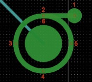 |
| Figure 9-108 Adding a guard ring around a pin. |
Adding Ground Planes to Routing Layers
Next we add Ground planes to the top and bottom Routing layers.
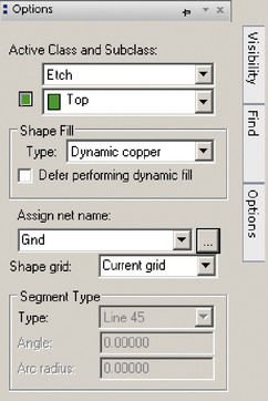
To add Ground plane areas to a routing layer, make the Top (or Bottom) Etch layer active and select either the
ShapeAdd button,
 , or the
ShapeAddRect button,
, or the
ShapeAddRect button,
 . Display the
Options tab and select
Dynamic copper and assign the GND net to the shape, as shown in
Figure 9-109
.
. Display the
Options tab and select
Dynamic copper and assign the GND net to the shape, as shown in
Figure 9-109
.
| ShapeAdd button
|
| ShapeAddRect button
|
 |
| Figure 9-109 Selecting Etch properties for a ground area on a routing layer. |
Left click to place the first vertex. If placing a rectangle, left click the opposite corner to complete the plane. If you are placing a polygon, left click to place other vertices to define the boundaries of the plane. To finish the polygon, right click and select
Complete from the pop-up menu.
An example of a copper plane is shown in
Figure 9-110
. Notice that thermal reliefs are automatically placed on pins and pads. The spacing of the plane to the pad (pin) and the spoke width are set using the rules in the Constraint Manager.
 |
| Figure 9-110 An example of a poured ground plane on a routing layer. |
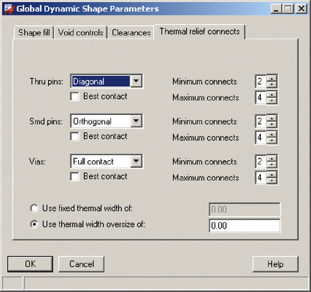
Thermal reliefs are set to orthogonal (+) by default, but you can change them to diagonal (×) if you prefer.
To change the direction of thermal reliefs on a positive Plane (Routing) layer, select
Setup → Design Parameters from the menu bar. In the
Design Parameter Editor dialog box, select the
Shapes tab then select the
Edit Global Dynamic Shape Parameters… button. In the
Global Dynamic Shape Parameters dialog box (see
Figure 9-111
), select the
Thermal relief connects tab and choose the desired direction.
 |
| Figure 9-111 Setting thermal relief properties for a positive plane. |
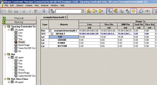
To change the spacing of the Ground plane to pins on a Routing layer, launch the Constraint Manager and select the
Spacing tab (
Figure 9-112
). Select the
Shape icon under the
Spacing Constraint
Set folder and select the
TOP layer (or whichever layer you want to change). Change the
Shape to Line,
Shape to Thru Pin, and so forth settings to the desired width. Changes are effective immediately; however, if your plane areas were not drawn using dynamic copper, your design may look as if something has gone horribly wrong.
 |
| Figure 9-112 Setting trace to copper pour spacing rules. |
If the ground plane on the Top layer suddenly takes over, the design is actually OK, the shapes just need to be updated.
To update the Ground plane shape, select
Display → Status from the menu bar. In the
Status dialog box (
Figure 9-113
), select the
Update to Smooth button. The Ground plane should now look correct again and have the proper spacing.
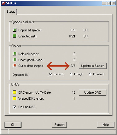 |
| Figure 9-113 Use the
Status dialog box to update shapes. |
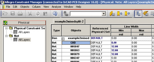
To change the spoke width of thermal reliefs on a routing layer, select the
Physical tab in the Constraint Manager (see
Figure 9-114
). Select the
All Layers icon under the
Net folder. Change the line width of the net that has the thermal reliefs you are interested in. The spokes and traces will now be the same for the nets you modify. Perform the Update Shapes step as described previously to update your board design. If you need to have certain trace widths for specific segments on a net and you do not want to have these changes affect them, you must go back and change those segments back to the way you want them using the Change command (in the
Edit menu) and the
Options and
Find filter tabs. Once the changes have been made, you can then
Fix them so that the changes are not undone.
 |
| Figure 9-114 Use the Constraint Manager to control thermal relief spoke width on routing layers by changing the trace line width. |
Once your plane is established, remember to place voids and merge copper areas and the like on the new plane to match the inner Ground plane as appropriate. Update the DRC to make sure the copper pour did not cause any errors.
You can add a Ground plane to the Bottom layer (or any other Routing layer for that matter) using the same procedures used for the Top layer. When you have several Ground planes, it is important that they have many low-impedance connections to help keep the planes at the same potential throughout the board area. This is done by placing vias, which are connected to the net for those planes, at various places. These vias are sometimes called
stitching vias. To place stitching vias on a board to connect multilayer Ground planes, select the Add Connection tool, left click on the plane that needs the via (a trace will be started), right click and select
Add Via from the pop-up menu.
To place multiple vias, use the Copy Button,
 to copy the via and left click wherever you want a via placed (right click and select
Done to quit). An example is shown in
Figure 9-115
. It is also a good idea to place a couple of vias underneath the ADC (U2).
to copy the via and left click wherever you want a via placed (right click and select
Done to quit). An example is shown in
Figure 9-115
. It is also a good idea to place a couple of vias underneath the ADC (U2).
| Copy Button
|
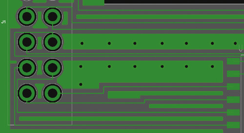 |
| Figure 9-115 Use stitching vias to provide good connections to ground planes. |
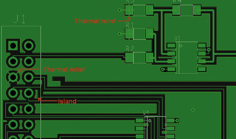
If you look closely at the ground strips between some of the traces and between some of the pins on the connector, J1, in
Figure 9-110
and
Figure 9-115
, you will notice that some areas are isolated from the rest of the Ground plane. These isolated strips are called
islands. Islands can act like antennas, which can pick up high-frequency noise (EMI) and cause problems for the rest of the circuit. To solve this problem, the strips and islands need to be either tacked down to the Ground planes using the stitching vias, trimmed, or removed altogether.
Use vias as just described to tack the strips to the underlying Ground plane. For parts of strips or islands that you want to trim from larger, stitched sections, use one of the Shape Void tools to remove unwanted sections of the strip.
To trim islands and isolated strips, select one of the Shape Void tools and use the
Options tab to select the correct layer and net to void. Select the shape, then draw the void shape over the area you want removed.
To completely remove strips or islands, use the Island_Delete tool,
 . By default all islands on a layer associated with a particular net will be deleted. Use the
Options tab to select whether to delete all the islands on that layer or just specific ones.
To delete only specific islands, select the
First button on the
Options tab then left click on the island you want to delete. Right click and select
Done when finished.
. By default all islands on a layer associated with a particular net will be deleted. Use the
Options tab to select whether to delete all the islands on that layer or just specific ones.
To delete only specific islands, select the
First button on the
Options tab then left click on the island you want to delete. Right click and select
Done when finished.
| Island_Delete tool
|
This completes Design Example 2.
..................Content has been hidden....................
You can't read the all page of ebook, please click here login for view all page.