Example 1. Dual Power Supply, Analog Design
The first example demonstrates the basics of schematic entry in Capture, including finding and placing parts, connecting parts and using global power nets, and generating a bill of materials to assist in the design process. The example continues with PCB design in PCB Editor and demonstrates how to specify board requirements, such as trace width and spacing, and setting up the overall board design; how to define layers; and how to perform manual and automatic routing.
To follow the example exactly as it is presented here, you need to copy the footprints for this example from the Web site for this book. Copy the contents of the symbols file folder located in the
Projects/Analog_Ex folder (
Figure 9-1
).
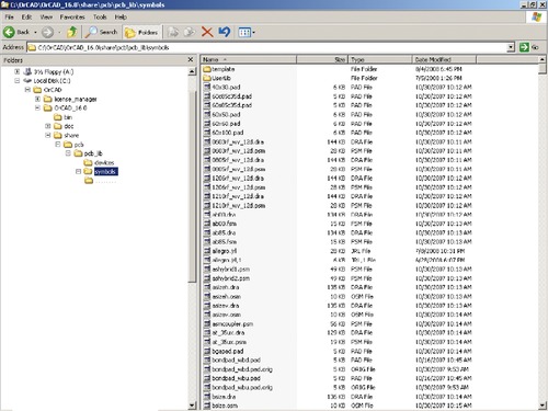 |
| Figure 9-1 Location of the PCB Editor footprint library. |
Although all the schematic and design files for this example are also included on the Web site, you need not copy them, because all the Capture parts in the example are already included with the OrCAD software. However, if you choose to copy the design files simply copy the entire
ANALOG_EX folder into your project folder. If you have not set up a project folder, now would be a good time to set one up. You can set it up anywhere your computer has access to it, and OrCAD should have no problem with it.
Before you start a PCB design process, you will likely have some sort of preliminary design concept jotted down. Perhaps PSpice simulations of sections of the design have even been performed. The design concept for this example is shown in
Figure 9-2
.
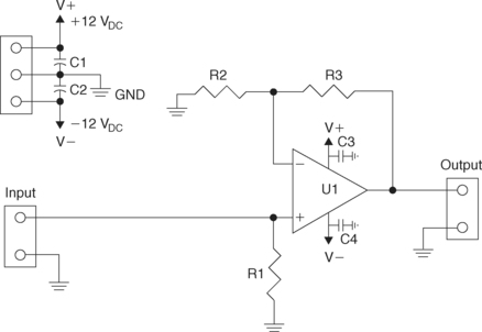 |
| Figure 9-2 Analog circuit for design Example 1. |
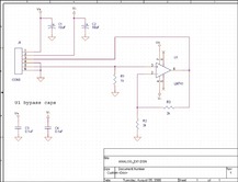
The circuit is very simple, but it contains enough parts that it encompasses the same steps required for larger, more complicated designs. The circuit is a basic amplifier that consists of an active component (the op amp) and several passive components (resistors and capacitors). The circuit also con-tains an off-board connector that supplies dual rail power to the board and connections for input and output signals. Through-hole components include the connector and power supply filter capacitors, surface-mounted devices include the op amp, its bypass caps, and the signal conditioning and gain resistors.
Once you have the basic design down, you need to make a list of all the parts needed to build the circuit, including the off-board connector. Search through your favorite parts catalog to find the parts and download the data sheets from the manufacturers. It is helpful to make a spreadsheet that details the parts and footprints to keep track of the design details throughout the design flow, so that once you receive the board from the manufacturer, the parts fit properly. An example spreadsheet is given in
Table 9-1
. During the entire design process, you can continually add information to the spreadsheet to document and organize all aspects of the design process. If a problem does occur, the documentation can help identify where the fault occurred.
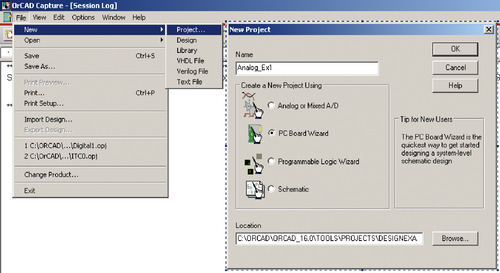
To begin a new design project, start Capture and, from the session window’s
File menu, choose
New → Project. At the
New Project dialog box (
Figure 9-3
), enter a name for the project. Select the
PC Board Wizard radio button. You can also make PCB designs if you select the
Analog or Mixed A/D button, which sets up PSpice simulation templates for the project. Since we are not performing PSpice simulations in this example,
PC Board Wizard is used. Select the desired location for your project, then click
OK.
 |
| Figure 9-3 Setting up a new project with the
PCB Project Wizard. |
At the next
Project Wizard dialog box, do not enable project simulation, click
Next. At the next dialog box, add the
Connector,
Discrete, and
OPAmp part libraries as shown in
Figure 9-4
. To add a library, select it (by clicking on it) in the left box and press the
Add>> button. After you have added the libraries you want, click the
Finish button.
 |
| Figure 9-4 Adding parts libraries to the project. |
If you are using the demo edition, you will be shown an information box that says,
The Demo Edition does not support saving to a library with more than 15 parts…. Click
OK each time it asks (you will need to click once for each library that you added to the project).
DRAWING THE SCHEMATIC WITH CAPTURE
Figure 9-5
shows the design goal. You can use it as a reference through the design example or modify it to your liking. If you are using the demo version, remember that you cannot save a design in PCB Editor that has more than 10 parts or parts with more than 14 pins. This design example meets these requirements so that you can save your work.
 |
| Figure 9-5 Analog circuit schematic design in Capture. |
If a schematic page does not automatically open, expand the
Design icon and the schematic folder in the
Project Manager window, then double click the
Page1 icon.
PLACING PARTS
Before placing any parts onto the schematic page, make sure that the place grid is enabled. If parts are placed off grid, you will not be able to connect wires to the part’s pins. Use the Search tools just described to locate and place parts on the schematic page.
Table 9-2
lists the parts used in this project and the libraries in which they are located.
To place parts click the
Place Part tool button,
 ; select
Part from the
Place menu; or hit the
P key on your keyboard. In the
Place Part dialog box (see
Figure 9-6
), select the
OPAMP library or the
EVAL library (if using the demo version), and scroll down until you find the LM741 or the uA741 op amp, respectively. Either one will work; it is just a matter of which one you prefer. You can place one of each, compare them, then delete the one you do not like. If a library is not shown in the
Libraries: box, you can add it to the list, as explained next. Once you find and select the part, click
OK.
; select
Part from the
Place menu; or hit the
P key on your keyboard. In the
Place Part dialog box (see
Figure 9-6
), select the
OPAMP library or the
EVAL library (if using the demo version), and scroll down until you find the LM741 or the uA741 op amp, respectively. Either one will work; it is just a matter of which one you prefer. You can place one of each, compare them, then delete the one you do not like. If a library is not shown in the
Libraries: box, you can add it to the list, as explained next. Once you find and select the part, click
OK.
| Place Part tool button
|
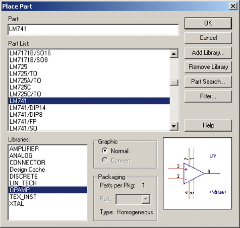 |
| Figure 9-6 Choosing parts from the
Place Part dialog box. |
If a library is not displayed in the
Libraries: window, you need to add it to the list.
To add a library to the
Libraries: list in the
Place Part dialog box, click the
Add Library… button on the
Place Part dialog box (
Figure 9-6
). Use the
Browse File dialog box to locate the desired
OLB library. For building schematics and PCB layouts, you can use parts from either the main
Capture library folder or the
PSpice subfolder. If you are performing PSpice simulations, select parts only from the
PSpice folder.
From the
DISCRETE library, place two polarized capacitors (
CAP POL), two nonpolarized capacitors (
CAP NP), and three resistors (
R). From the
CONNECTOR library, place a six-pin connector (
CON6), and from the
OPAMP library, place
LM741.
CONNECT PARTS WITH WIRES (SIGNAL NETS)
To wire the circuit, use the Place Wire tool,
 ; select
Wire from the
Place menu; or hit
W on your keyboard to activate the Wire tool. To attach wires between pins, click once to start a wire, move the pointer to the next pin and click once to attach the wire, and continue routing or double click to end the wire. Connect the circuit as shown in
Figure 9-5
.
; select
Wire from the
Place menu; or hit
W on your keyboard to activate the Wire tool. To attach wires between pins, click once to start a wire, move the pointer to the next pin and click once to attach the wire, and continue routing or double click to end the wire. Connect the circuit as shown in
Figure 9-5
.
| Place Wire tool
|
MAKING POWER AND GROUND CONNECTIONS
There are three ways of adding power connections to active parts, depending on the part’s type of power supply pins. A part’s power supply pin can be a power-type pin and nonvisible, a power-type pin and visible, or a nonpower-type pin (such as a passive or input pin), which is always visible. The term
visible specifically refers to whether the pin is visible to the Wire tool. However, in the general case, a nonvisible pin is also invisible from the user’s perspective. Digital parts typically have nonvisible power pins, while analog parts, particularly op amps, commonly use either visible power pins or one of the nonpower-type pins (which are always visible).
If a part’s power supply pin is a power pin and is not visible, you cannot connect a wire (a net) to it directly. A nonvisible power pin is a net and it is global. You connect a part’s power pin to a power symbol by giving the pin and the power symbol the same name. To make the connection, you need to place a power symbol, which is also global, somewhere on the schematic. Power symbols are always visible and are wired to either an off-board connector or a PSpice power supply. To make the names the same, you can change the name of the power symbol, the power pin, or both. An example of how to do this is given next.
If a power supply pin is a power pin and it is visible, you can either take advantage of the power pin’s global properties using power symbols or make direct connections to it with wires. If you use the pin’s global nature, the pin name and the power symbol name must be the same, as described already. If you make a direct connection to the power pin with a wire, you need not consider the naming convention. If you have a multipart package (e.g., a quad op amp with shared power pins), all the parts within the package that are placed on a schematic must have their power supply pins connected in the same way. So either all must be global or all must have wires connected to them.
If a part’s power supply pin is a not a power pin (see LT1028 in the
LIN_TECH library, for example), you must use a wire to connect the pin to some other object, such as a power symbol or an off-board connector. If you place more than one part from a multipart package that has nonpower-type power pins, connections need to be made to only one of the part’s power supply pins (although you can make connections to all of them if you want). See
Chapter 7
for more information on pin types.
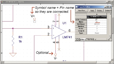
The LM741 op amp used in this example has visible power supply pins, so we could use their global properties by using power supply symbols to make connections to the off-board connector, but we will add the power supply symbols to the amplifier to make it evident from the schematic what power the amplifier uses. Whether you used the LM741 from the
OPAMP library or the uA741 from the
EVAL library, both power supply pins are visible power pins. The difference in their appearances is that the uA741 has zero-length power pins and the LM741 has line-length power pins. A zero-length pin is still “visible” to the Wire tool but not to the user.
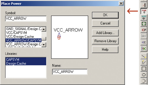
To place power symbols, click the
Place Power tool button and select one of the power supply symbols (
VCC in this example) from the
Place Power dialog box, as shown in
Figure 9-7
. Click
OK and place the symbol onto the schematic.
 |
| Figure 9-7 Placing global power symbols. |
The names of the power pins on the op amp and the names of the power symbols must be the same. You can change the name of the symbol or the pin or both. Some parts have no visible labels for their power pins.
To check a pin’s name and type, select the pin (if it is visible), right click, and select properties at the pop-up menu to get a
Property Editor dialog box for the pin (see
Figure 9-8
).
 |
| Figure 9-8 Using the part
Property Editor to change a pin’s name or type. |
To change the name or type of a nonvisible power pin, select the part on the schematic, right click, and select
Edit Part from the pop-up menu. You will be given a Capture
Part Editor window (see
Figure 9-9
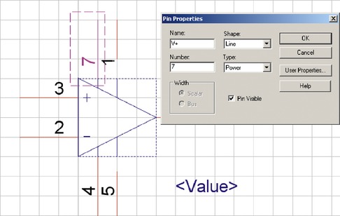
). Double click the pin whose name you want to change to bring up the
Pin Properties dialog box as shown in
Figure 9-9
. Enter the new name in the Name: text box and click
OK. Repeat the process for the other power supply pin.
 |
| Figure 9-9 Determining a power pin’s type and name. |
Close the Part Editing window. Click
Update Current when Capture asks Would you like to update only the part instance being currently edited, or all part instances in the design? In this case, since there is only one LM741, it does not matter if you click
Update Current or
Update All. But if you had several LM741s and you did not want all of them to have their power pin names changed, you would click
Update Current.
Note: When you change a part on the schematic, the link between the design cache and the part library is broken. See the section at the end of the chapter for details on managing the design cache.
Instead of changing the name of the power pin on the part, you can change the name of the power supply symbol.
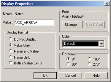
To change the name of the power supply symbol, double click the symbol’s name on the schematic. The
Display Properties dialog box will pop up, as shown in
Figure 9-10
. The op amp’s positive power supply pin name is V+, so enter V+ in the Value: text box then click OK. Place another power supply symbol and change its name to V− using the same procedure. Copy, place, and connect the V+ and V− power symbols as shown in
Figure 9-5
.
 |
| Figure 9-10 Use the Display Properties dialog box to change a power symbol’s name. |
Next, add a ground symbol.
To place a ground symbol, click the
Place Ground tool button, and select one of the ground symbols from the
Place Ground dialog box. Click
OK and place the symbol onto the schematic. Place and connect ground symbols as shown in
Figure 9-5
.
Note: For designs that will be simulated with PSpice, you must use a GND symbol named 0 for the circuit to simulate correctly. You can use any of the symbols as long as they have the name 0. For PCB designs that will not be simulated, you can use any of the GND symbols and name them whatever you want. A separate net will be instantiated for each distinct GND name. See Examples 2 and 3 for techniques on how to establish multiple GND systems.
Preparing the Design for PCB Editor
Once all of the connections have been made, the next step is to prepare the design for making a netlist.
Things to do:
▪ Make sure all of the footprints are assigned.
▪ Assign parts to groups (called rooms).
▪ Perform an annotation.
▪ Clean up the design cache.
▪ Perform a DRC in Capture.
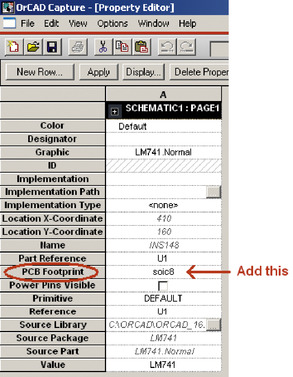
There are several ways to find out which (if any) parts have footprints assigned to them and if they are the right ones. You can check each part one at a time by double clicking a part to bring up the properties spreadsheet and look at the
PCB Footprint cell, as shown in
Figure 9-11
. Or you can check all the parts at the same time by selecting all the parts in the schematic (drag a box across the schematic using the left mouse button), then right click and select
Edit Properties… from the pop-up menu. The spreadsheet will show the properties of all the parts that were selected. To toggle the spreadsheet view between the column and row organization, right click the upper left corner or the spreadsheet and select
Pivot from the pop-up menu.
 |
| Figure 9-11 Part properties spreadsheet. |
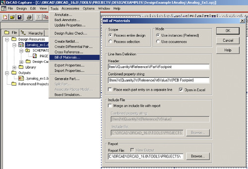
The spreadsheet method is fast and easy for small circuit designs, but it may be impractical for large circuits. An alternative is to generate a customized BOM that lists all the footprints in an Excel spreadsheet. The spreadsheet can be printed and used as a reference while you are searching through the footprint symbol library for the right footprints.
To generate the custom BOM, go to the
Project Manager, select the
Design icon, and then select
Bill of Materials… from the
Tools menu (see
Figure 9-12
). At the
Bill of Materials dialog box, add the text
Footprint in the text box labeled
Header: and add the text
{PCB Footprint} in the text box labeled
Combined property string:. Put a check mark in the
Open in Excel box. You can specify the location and name of the BOM using the
Browse… button at the bottom. Click
OK when you have finished the setup.
 |
| Figure 9-12 Generating a bill of materials to include PCB footprints. |
The next step is to assign footprints to the components. To find footprints in
PCB Editor’s footprint
libraries, navigate to the
C:OrCADOrCAD_16.0sharepcbpcb_libsymbols folder (see
Figure 9-1
). Footprints have the *.dra and *.psm file extensions. When you find the footprint you are looking for, either memorize it or copy the name (without the extension) to the Windows clipboard.
Go back to Capture. To assign the footprint to a part, display the properties spreadsheet for the part to which you want to assign the footprint (double click the part to display its properties spreadsheet). Type or paste the footprint name (without the file extension) into the
PCB Footprint cell in the properties spreadsheet (see
Figure 9-11
).
If several parts have the same footprint (the capacitors and resistors, for example), you can change all of them at the same time.
To assign a footprint to multiple parts simultaneously, hold down the
Ctrl key on your keyboard while you select each component, right click, and select
Edit Properties… from the pop-up menu. Select the
PCB Footprint column (or row if the spreadsheet is pivoted) to select all of the PCB footprint cells then right click and select
Edit… from the pop-up menu to display the
Edit Property Values mini spreadsheet shown in
Figure 9-13
. Paste the footprint name that you copied from PCB Editor into the
PCB Footprint cell then click
OK. Once you have all of the footprints assigned, you can generate another bill of materials, so that you can see all of the footprints at the same time to make sure you have not missed any.
Figure 9-14
shows the final BOM listing with all the footprints assigned.
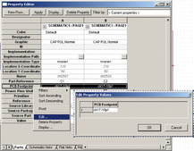 |
| Figure 9-13 Assigning footprints to multiple parts with the
Property Editor. |
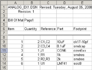 |
| Figure 9-14 Final BOM listing with all footprints assigned. |
You can also use the Find tool to automatically select a part or parts of a certain type. To use the Find tool select
Find from the
Edit menu; the
Find dialog box will be displayed as shown in
Figure 9-15
. If you enter R1 in the
Find What: text box, R1 will be highlighted on the schematic and centered on the screen. If you enter
R*, then all resistors will be selected. You can use the Find tool to look for other things, such as text and nets, as indicated in
Figure 9-15
.
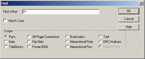 |
| Figure 9-15 Using the Find tool to locate parts. |
Grouping related components in the schematic can make placing the parts easier in PCB Editor. Parts are assigned a room number in Capture, and the grouping information is exported to PCB Editor during netlist generation (and ECO processes).
To add parts to a group, select the related parts (e.g., J1 and the two filter caps) on the schematic. Right click and select
Edit Properties from the pop-up menu to display the
Property Editor spreadsheet (see
Figure 9-16
). In the
Filter by: dropdown list, select
Cadence-Allegro. Select the
ROOM cell to select that property for all of the components then right click and select
Edit from the pop-up menu. In the
Edit Property Values dialog box, assign an integer number or any alpha-numeric characters for the group (this will be the room name PCB Editor uses). Click
OK to close the dialog box. The alpha-numeric value will be assigned to all the parts you selected. Close the spreadsheet.
 |
| Figure 9-16 Using the
Property Editor to assign components to groups (Rooms). |
You can also add the room property to the bill of materials listing by adding
Room to the
Header: list and
{ROOM} to the
Combined Property String list.
Before making the netlist, it is a good idea to tidy up the design by performing an annotation, cleaning up the design cache, and performing a DRC as described next.
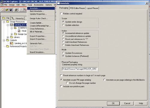
ANNOTATION
Performing an annotation chronologically renumbers the part references in your schematic design from top to bottom.
To perform an annotation, go to the Project Manager and select
Annotate from the
Tools menu. The
Annotate dialog box shown in
Figure 9-17
is displayed. Select the items you want updated then click
OK. Be sure to check multipart components (hex inverters, for example) to make sure that they are annotated correctly.
 |
| Figure 9-17 Performing a design annotation. |
CLEANUP CACHE
Cleanup Cache removes unused parts from the design cache. Unused parts pile up in the design cache when you place parts in the design then later delete them. To clean up the design cache, select the
Design Cache folder in the Project Manager, right click, and select
Cleanup Cache from the pop-up menu or select
Cleanup Cache from the
Design menu.
PERFORMING A SCHEMATIC DRC IN CAPTURE
It is a good idea to run a DRC before generating a netlist. The DRC checks your design for design rule violations and places error markers on the schematic page.
To perform a DRC in a Capture project, make the
Project Manager window active. From the
Tools menu, select
Design Rules Check…. The
Design Rules Check dialog box is displayed as shown in
Figure 9-18
. Select the items you want to check and click
OK. If you have errors, you can search for the markers by using the
Browse DRC Markers command from the Project Manager’s
Edit menu or from the
Find option on the schematic’s
Edit menu.
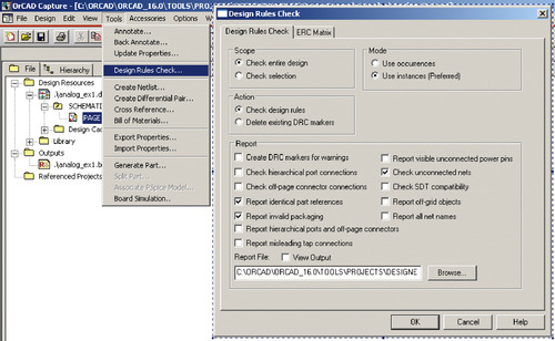 |
| Figure 9-18 The Capture
Design Rules Check dialog box. |
You can refine what the DRC looks for and how it reports its findings (as errors,
E, or warnings,
W) using the
ERC Matrix tab in the
Design Rules Check dialog box. As shown in
Figure 9-19
, the matrix lists pin types on the left side and along the slanted side. The yellow
W and red
E boxes indicate the result of having pins of certain types connected together. For example, an output pin connected to another output pin will produce an error during a DRC, but a passive pin connected to an output pin will not cause an error or a warning. You can change the boxes by clicking on them with the left mouse button. By clicking on a button repeatedly, you can toggle through the three options: warning, error, or neither.
 |
| Figure 9-19 The DRC error type selection matrix. |
GENERATING THE NETLIST FOR PCB EDITOR
Once you have all of your connections finished and footprints and rooms assigned, you can create the netlist for PCB Editor.
To create a netlist for PCB Editor, select the
Design icon in the Project Manager and select
Create Netlist… from the
Tools menu. In the
Create Netlist dialog box (see
Figure 9-20
), select the
PCB Editor tab and specify a netlist name or accept the default name. Select the
Create PCB Editor Netlist and the
Create or Update PCB Editor Board (Netrev) boxes. You can specify an
Input Board File if you have one (such as a board template or preexisting board design), or you can leave it blank. A default
Output Board File will be set up for you, or you can specify your own. Select the
Open Board in PCB Editor radio button and then click
OK.
PCB Editor will automatically start.
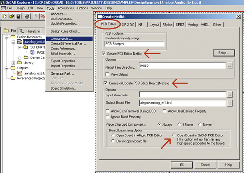 |
| Figure 9-20 Creating a circuit netlist for
PCB Editor from Capture. |
PROBLEMS DURING NETLIST CREATION
During the netlist creation, you may experience success, success with warnings, or failure. If there are problems, OrCAD will tell you to look at the
netrev.lst file to find out what the problems were. The
netrev.lst file is located in the folder where the board resides. When you open the file, you will be presented with the
File Conversion dialog box shown in
Figure 9-21
. You can scroll down and look for the error in the preview pane or open the entire document.
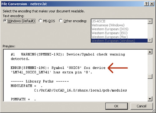 |
| Figure 9-21 Using the
netrev.lst file to find netlisting errors. |
In this example an error occurred because the Capture part has one fewer pins than the PCB Editor footprint symbol. Since this is not a fatal error, the netlist process was completed and PCB Editor will be launched. If a fatal error occurs, PCB Editor will still be launched, but the netlist process will not be completed properly and no information will be transferred to PCB Editor. In this case, though, the error will prevent placing the U1, so we need to go back and modify the schematic. We use this error as an opportunity to show how to perform an ECO later in the example.
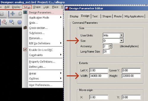
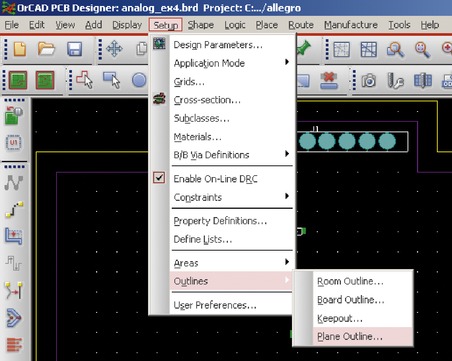
Setting Up the Board
The first view you have of your new board will be PCB Editor with a black background in the work area. The next steps are to set up the board outline and define some of the basic design parameters.
SETTING UP THE EXTENTS (WORK AREA BOUNDARY)
The default size of the work area is 34
in.×22
in. (size D). If the drawing area is much larger than it needs to be, that can make navigating around and working on your project harder than if the drawing area size is just right.
To change the size of the work area, go to
Setup → Design Parameters, and change drawing size or change the
X and
Y Extents on the
Design tab of the
Design Parameters dialog box, as shown in
Figure 9-22
. Make sure you click
Apply to make the changes take effect, then click
OK.
 |
| Figure 9-22 Setting up the board extents. |
CONTROLLING THE GRID
The next step is to turn on the grid.
To turn the grid on, click the
Grid button,
 .
To change the grid spacing, select
Grids… from the
Setup menu; the
Define Grid dialog box will be displayed (see
Figure 9-23
). There are two grid systems: one for copper elements (
Etch) and one for everything else (
Non-Etch). You can change the etch grids on each layer individually or change them all simultaneously by using the
All Etch entries. Click
OK to dismiss the dialog box when you are finished.
.
To change the grid spacing, select
Grids… from the
Setup menu; the
Define Grid dialog box will be displayed (see
Figure 9-23
). There are two grid systems: one for copper elements (
Etch) and one for everything else (
Non-Etch). You can change the etch grids on each layer individually or change them all simultaneously by using the
All Etch entries. Click
OK to dismiss the dialog box when you are finished.
| Grid button
|
 |
| Figure 9-23 Setting the design grids. |
MAKING A BOARD OUTLINE
The next step in laying out the board is to make the board outline and add mounting holes so that the boundaries of the board are known.
First we draw the board outline. Zoom in an appropriate amount so that your final board size will take up about 75% of your display’s viewing area (large enough for good resolution but small enough that you can see the whole thing.). To change zoom, select one of the zoom options from the
View menu, or select one of the
Zoom buttons on the toolbar.
To place a board outline, select
Setup → Outlines → Board Outline… from the menu bar. The
Board Outline dialog box will be displayed, as shown in
Figure 9-24
. In the basic example in
Chapter 2
, we just drew a box. This time we draw an irregular shape using the polygon tool. Click the
Draw Polygon radio button in the
Board Outline dialog box then left click and release once in the work area at the starting vertex of the board. Left click at point 0, 0 to place the first vertex. Left click to place each vertex of the board outline. Make the board outline about 5.0×3.0
in. (5000×3000
mils). Left click and release at each vertex. To finish the board, click on the starting point again to close the polygon. The board outline will be a dashed line with squares (handles). You can use the handles to resize or change the shape of the board outline. If the board outline is correct, then click the
OK button to dismiss the
Board Outline dialog box. The example board outline is shown in
Figure 9-25
.
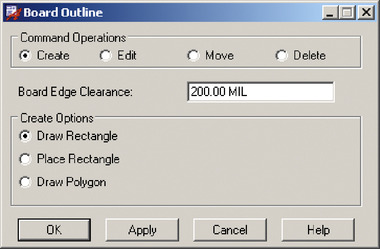 |
| Figure 9-24 The
Create Board Outline dialog box. |
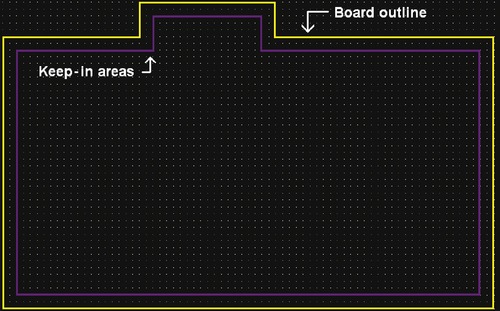 |
| Figure 9-25 The finished board outline and keep-in areas. |
ADDING DIMENSION MEASUREMENTS
You can add dimension lines and measurements to your board for documentation purposes. You can also add temporary construction lines as guides to mark locations for mounting holes and connectors and the like. Dimensions are placed on the
BoardGeometry/Dimension layer (class/subclass), so once you are satisfied with the board layout, you can turn off that layer to hide the dimension objects or delete temporary construction lines.
For this example we add dimension lines to mark a mounting hole location. First set the grid spacing for nonetch to 10
mils (see
Figure 9-23
). Next you may want to change the coordinate indication (
XYMode) to absolute or relative depending on the dimension you are using. To change the
XYMode, click the
R or
A button at the bottom of the design window (see
Figure 9-26
).
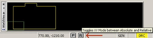 |
| Figure 9-26 Toggle between absolute and relative
XY modes. |
To place a dimension line, select
Dimension/Draft from the
Manufacture menu and from the menu choose the desired dimension type.
Figure 9-27
shows the available dimensioning tools. A linear dimension is demonstrated here.
 |
| Figure 9-27 Dimensioning tools. |
Left click to place the first dimension point (point 1
in
Figure 9-28
), left click to place the end mark (point 2
in
Figure 9-28
), and finally left click to place the location of the text (point 3
in the figure). Use the
XY coordinates to precisely place the dimensions. You can also just pick a line object, and the dimension tool will automatically measure it and place the end points for you.
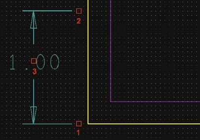 |
| Figure 9-28 Linear dimension line and pick points. |
You can also use the Add Line,
 , and Add Rectangle,
 , tools to add construction lines, etc. to your design on the
BoardGeometry/Dimension layer.
, tools to add construction lines, etc. to your design on the
BoardGeometry/Dimension layer.
| Add Line
|
| Add Rectangle
|
You can change dimension parameters such as text size and arrow terminations.
To change the appearance of the dimension lines, select
Manufacture → Parameters from the menu bar to display the
Drafting dialog box, from which you can change various aspects of the dimension elements through the dialog boxes shown in
Figure 9-29
.
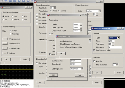 |
| Figure 9-29 Controlling dimensioning parameters. |
Once you place a dimension and end the command, the dimension object is nondynamic. This means that you can move it, but it will not be updated with new dimension information. If you need to change or move a dimension line to measure a new parameter, you have to place a new one.
ADDING MOUNTING HOLES
Next we place mounting holes on the board. This should be done before moving any parts into the board outline.
To place mounting holes, select
Place → Manually from the menu bar and select
Mechanical symbols from the
Placement list as shown in
Figure 9-30
. If no symbols are listed, check to make sure you have the
Library box checked in the
Advanced Settings tab.
 |
| Figure 9-30 Placing mounting holes on the board. |
Select the desired mounting hole symbol (it must be in the library ahead of time). Left click at the desired location in the work space to place the mounting hole. Only one will be placed per click. To add additional holes, recheck the desired symbol and left click again.
To add multiple mounting holes, you can copy and paste instead of using the placement method. To copy a mounting hole, click the
Copy button (or type
copy in the command line and hit the
Enter key). The command window will say
Select elements to copy:. Use the left mouse button to drag a box across an existing mounting hole (to select all elements of it). The command window then will say
Pick user-pick origin. Click on the object (or near it) to get a handle on it. Left click to place one or more copies of the mounting hole. When you are finished placing the mounting holes, right click and select
Done from the pop-up menu.
To delete a mounting hole click the
Delete button (or type
delete in the command line and hit the
Enter key). The command window will say nothing. Use the left mouse button to drag a box across an existing mounting hole (to select all elements of it). Right click and select
Done from the pop-up menu. Alternatively you can use the left mouse button to drag a box across an existing mounting hole (to select all elements of it). Right click and select
Symbol → Unplace component.
The mounting holes supplied with PCB Editor are nonplated. Nonplated holes are drilled separately as one of the very last steps of the board fabrication and no plating processes occur after the final drilling. See
Chapter 8
on designing mounting holes and Appendix D for standard machine screw and drill hole sizes. To make mounting holes plated, select
Tools → Padstack → Modify Design Padstack from the menu bar, left click the mounting hole to select it, right click, and select
Edit from the pop-up menu; the
Padstack Designer dialog box will be displayed as shown in
Figure 9-31
. In the
Drill/Slot hole section, you can select whether the hole is plated or not.
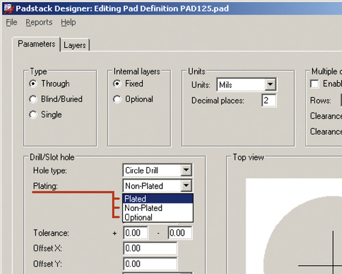 |
| Figure 9-31 Using
Padstack Designer to determine hole plating. |
You can leave a mounting hole isolated from the copper on all layers, or if it is a plated mounting hole, you can connect it to a net (e.g., the Ground plane). To connect a plated mounting hole to a net, you need to add a single pin part to the design in Capture then connect the part’s pin to the desired net. The mounting hole will become part of the netlist. Then in PCB Editor the mounting hole can be placed in the same manner as all the other parts, as described later, and it will be connected to the proper net. This is demonstrated in the manufacturing design example in
Chapter 10
. Along with making a part in Capture, you also need to make a footprint with a connect pin (rather than a mechanical symbol with a mechanical pin) for the mounting hole in the PCB Editor footprint library (see
Chapter 8
for details).
PLACING PARTS
Placing parts is part art and part science. How you ultimately place the parts on the board depends on both mechanical and electrical factors. Mechanical factors include designing for manufacturability (assembly and soldering processes) and physical board constraints (size, shape, etc.). Electrical factors include functional signal flow, thermal management, signal integrity, and electromagnetic compliance. Usually all these considerations are important, and in some cases, they can conflict with one another. These issues are discussed in greater detail in
chapter 4
,
chapter 5
and
chapter 6
and in the IPC standards. In this example, the parts are simply placed so that the board layout is similar to the flow of the schematic.
Before you begin placing parts, you may want to adjust the placement grid resolution. Go to
Setup → Grid and change the
Non Etch Grid to 50
mils (or 25
mils for greater resolution, as suggested by IPC).
The three basic ways to place parts are manually, quick place, and through intertool communication (ITC). The easiest method for small projects is to use the manual method, as was shown in
Chapter 2
(i.e., select
Place → Manually from the menu bar, select the part or parts you want to place, and left click to place them). In this example we see how to use the quick-place method and the Intertool Communication tool to select parts for placement.
Note: Regardless of how you place the parts, you will likely have a problem placing U1 in this example if you used the default op-amp part in Capture and a default eight-pin footprint in PCB Editor. If this occurs we will see later how to fix the problem using the ECO function.
To use the quick-place method, select
Place → Quickplace… from the menu bar; the
Quickplace dialog box will be displayed (see
Figure 9-32
). There are many ways of selecting and filtering parts for placement. When using the
Placement Filter options, a property has to be assigned to a part or parts for that filter to work (e.g., a room has to be assigned to use the
Place by room filter). Note that there are similarities between the
Quickplace dialog box and the
Placement dialog box. When using the
Place by REFDES filter, the
Placement dialog box works better (it has more details options and allows you to see what parts match the filters), but the
Quickplace dialog box gives more control with the
Placement Position section options.
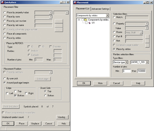 |
| Figure 9-32 Using the quick-place method to place parts. |
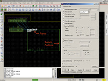
In this example we use the
Quickplace dialog box to place parts by rooms. Recall that rooms were assigned to parts in Capture; this is where we use that property. Before we do, though, we need to define areas on the board where the parts with common room numbers will be placed.
To define a room on the board, select
Setup → Outlines → Room Outline… from the menu bar. The
Place Outline dialog box will be displayed (see
Figure 9-33
). Also, if you look at the
Options tab, you will notice that the default class/subclass is
Board Geometry/ Both_Rooms (also indicated in the
Side of Board section, the
Both radio button is checked). In the
Place Outline dialog box, you can specify the room (group) that was assigned in Capture (i.e., the
Room Name). You can also select the room type. The options are
HARD,
SOFT,
INCLUSIVE,
HARD_STRADDLE, and
INCLUSIVE_STRADDLE, which determine how the DRCs are issued (see
Using the ROOM and ROOM_TYPE Properties in alegroplace.pdf, p. 24). With the
Place Outlinedialog box displayed, draw the outline. When finished, click the
OK button to dismiss the
Place Outline dialog box.
 |
| Figure 9-33 Creating a
Room outline. |
Once the room outlines are drawn, you can then use the
Place by room option to place parts. In the
Quickplace dialog box (or the
Placement dialog box), select the
Place by room option and select the desired room name, then click the
Place button. The parts that were assigned to that room name will be placed in the room outline (see
Figure 9-34
). You can then use the Move tool,
 , to move the parts around within the room.
| Move tool
|
 |
| Figure 9-34 Parts placed in a room using quick place. |
Note: Remember that U1 will probably not place properly because of the problem mentioned previously. This will be addressed later.
If you select a part and do a
Show Element, you will see the
ROOM property included as shown in
Figure 9-35
.
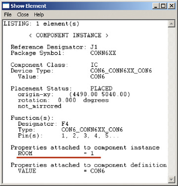 |
| Figure 9-35 Using Show Element tool to display a component’s room assignment. |
Intertool communication is a communication link between Capture and PCB Editor. This link allows you to perform two functions: cross-probing (also called
cross selection) and cross-highlighting. Cross-probing is used as an aid in placing components in PCB Editor (communication is from Capture to PCB Editor only). Cross-highlighting is a tool that allows you to visually highlight components, pins, or nets in one application and simultaneously highlight it in the other application (communication is bidirectional). To enable inter-tool communications, see
Figure 9-47
.
USING CROSS-PROBING TO PLACE PARTS
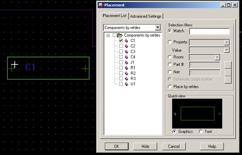
Depending on the complexity of your design it may be necessary to lay out specific parts of the board in a particular order or location on the board. In this case it might be easier to pick the specific parts from the schematic and have PCB Editor place those parts, and this is exactly what cross-probing does. For cross-probing to be enabled, you have to have your schematic open in Capture, your board layout open in PCB Editor, and be in manual placement mode in PCB Editor.
Prepare for cross-probing in PCB Editor by selecting
Place → Manually… from the toolbar to display the
Placement dialog box. From the dropdown menu, select
Components by refdes and, in the
Selection filters section, make sure the
Match: radio button is selected (see
Figure 9-37
later).
To begin cross-probing from Capture to PCB Editor, go to your schematic in Capture. Left click the part you want to place to highlight it (C1 in this example) then right click and select
PCB Editor select from the pop-up menu, as shown in
Figure 9-36
.
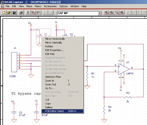 |
| Figure 9-36 Using cross-probing to place parts. |
Now go back to PCB Editor. That part will be checked in the dialog box and the part will be attached to your cursor, as shown in
Figure 9-37
. Left click to place the part. You can either click
OK (or right click and click
Done) to quit or go back to the schematic and select another part as just described.
 |
| Figure 9-37 The part selected in Capture is also selected in PCB Editor. |
ROTATING PARTS
To rotate a placed part, select the
Move button, left click to select the part, then right click; select
Rotate from the pop-up menu. The part will pivot around its origin, which may be pin 1 or the body center. Move the mouse around the pivot point until it is in the correct orientation. Use the
Options pane to select a different rotation criteria. Left click to place it, then right click and select
Done from the pop-up menu.
MIRRORING PARTS
If you want to move a part to the back side of your board, you mirror it.
To mirror a part, select the
Generaledit button (vice the
Etchedit button), left click to select the part, right click and select
Symbol → Mirror from the pop-up menu, as shown in
Figure 9-38
.
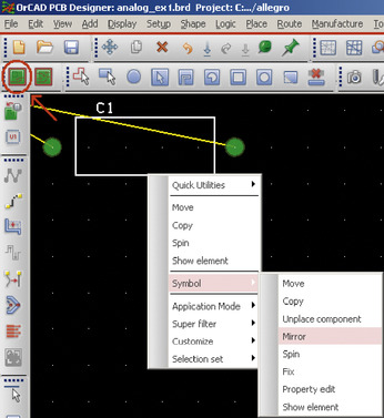 |
| Figure 9-38 Mirroring a placed component. |
As mentioned earlier U1 may not place properly because of the netlist warning that occurred during the netlist creation. The problem is that the part in Capture has only seven pins and the footprint in PCB Editor has eight pins. Every pin in a PCB Editor footprint must have a corresponding pin in the Capture part that is using it. So we either need to add a pin to the Capture part in the schematic or delete a pad in the PCB Editor footprint on the board. While it is possible to do the latter by deleting the connection type pin and installing a mechanical type pin, this would make that footprint useful for only that part or parts like it. You would need a different footprint for other op amps. This is true for SOT23 packages for diodes as well. So we change the part in Capture then perform an engineering change order (ECO) to update the board design.
CHANGING A PART IN CAPTURE
Go back to the schematic in Capture. Left click the op amp to select it. Right click and select
Edit Part from the pop-up menu.
In the part editor (see
Figure 9-39
), click the
Place pin button,
 . In the
Pin Properties dialog box, enter
NC (no connect) for pin name and the number
8 under pin number. Select the
Short and
Passive options. Click
OK and place the pin somewhere on the part boundary, as shown. You can also add a line to make the pin touch the body if you like or leave it floating, since it is a no-connect (NC) pin. And, in that case, it might be a good idea to add text indicating that, as shown in the figure.
. In the
Pin Properties dialog box, enter
NC (no connect) for pin name and the number
8 under pin number. Select the
Short and
Passive options. Click
OK and place the pin somewhere on the part boundary, as shown. You can also add a line to make the pin touch the body if you like or leave it floating, since it is a no-connect (NC) pin. And, in that case, it might be a good idea to add text indicating that, as shown in the figure.
| Place pin button
|
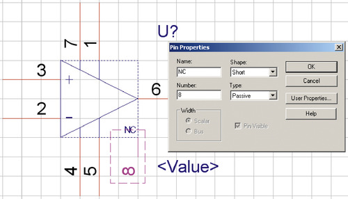 |
| Figure 9-39 Adding a no-connect pin to a part in Capture. |
Note: If a part has more than one NC pin, you have to give them different names (e.g., NC1, NC2, etc.) because a unique name is required for each pin; otherwise you will get a DRC error.
Once you finish modifying the part, close it by clicking the
X in the upper right corner of the part editor window. Click
Update Current (or
Update All if there are more than one of this type of part) when Capture asks
Would you like to update only the part instance being currently edited, or all part instances in the design?
Make sure that you place a no-connect symbol on the unused pin on the schematic.
PERFORMING AN ENGINEERING CHANGE ORDER (ECO)
Once the part has been changed on the schematic, the changes need to be updated in the board design. In PCB Editor, an ECO is used to update the board design with changes that were made to the schematic in Capture, whereas an update from PCB Editor to Capture is called
back annotation. Performing an ECO is a two step process: (1) recreate the netlist in Capture and (2) import the changes into the board in PCB Editor.
To perform an ECO, begin in Capture by making the
Project Manager window active. Highlight the
Design icon and then select
Tools → Create Netlist from the menu bar to display the
Create Netlist dialog box (
Figure 9-40
). So far this is the same process used to create the original netlist, but the next step is slightly different. In the
Options section below
Create or Update PCB Editor Board (netrev), use the
Input Board File: Browse… button,
 , to locate the current board you are working on (the one you want updated). Then use the
Output Board File: Browse… button to choose the location and name of the new updated board. You can update a board into itself, so the input board and the output board are the same, as shown in the figure. In the
Board Launching Option section, select
Do not open board file if your board file is already open, otherwise select
Open board in PCB Editor to open your board file. Click
OK.
, to locate the current board you are working on (the one you want updated). Then use the
Output Board File: Browse… button to choose the location and name of the new updated board. You can update a board into itself, so the input board and the output board are the same, as shown in the figure. In the
Board Launching Option section, select
Do not open board file if your board file is already open, otherwise select
Open board in PCB Editor to open your board file. Click
OK.
| Browse... button
|
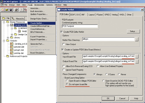 |
| Figure 9-40 Setting up for an ECO. |
If you selected
Open board in PCB Editor, the changes will be made automatically, but if you selected
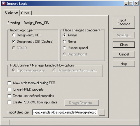
Do not open board file, then the board design must be updated with the changes.
If you relaunched PCB Editor from Capture, the board will be automatically updated with the new information. If you selected
Do not open board file, then you need to import the changes to update the board.
To update the design in PCB Editor, select
File → Import → Logic from the menu bar. The
Import Logic dialog box will be displayed. Select
Design entry CIS (Capture) in the
Import logic type section. Select the desired option in the
Place changed component section. Use the
Browse… button to locate the directory listed in the
Output Board File: (see
Figure 9-41
) if it is not already displayed. Click the
Import Cadence button to finish the ECO process. Your board should now have the updated information.
 |
| Figure 9-41 Import ECO information with the
Import Logic dialog box. |
Note: Depending on which version of the software you have, you may experience difficulties running the autorouter if you performed the ECO using the import logic method. If that occurs, save your design and close PCB Editor. Go back to Capture and perform another ECO, but launch PCB Editor from the
Create Netlist dialog box. You will not need to import logic again and the autorouter should work properly. If you are using the demo version, the autorouter is nonfunctional.
If you were not able to place the op amp, U1, you should be able to place it now. The quickest way to place the part is to select
Place → Manually from the menu (or click the
Place Manual button on the toolbar). U1 should be on the list; check it and place the part on the board; click
OK when you are finished.
Once the parts have been placed on the board, you need to position them. If all of the layers and nets are visible, it can be difficult to identify which parts are which. You can do a couple of things: turn off all or most of the nets and make only the necessary layers visible (e.g., silk-screen layers and pins).
CONTROLLING LAYER VISIBILITY
There are two methods for controlling layers (class/subclass) visibility. The first method is the
Options tab (
Figure 9-42
) and the second is the
Color dialog box (
Figure 9-43
).
To change the visibility of a layer using theOptionstab, move your mouse pointer over the
Options tab (if the pane is not displayed) and select the class and subclass of interest. Toggle the colored button to the left of the subclass to show or hide that subclass.
 |
| Figure 9-42 Use the
Options pane to control layer visibility. |
 |
| Figure 9-43 Using the
Color dialog box to control layer visibility. |
To change the visibility of a layer using theColordialog box, click the
Color button,
 , on the toolbar. Most of the layers are common to both the
Options tab and the
Color dialog box, but the
Color dialog box gives you access to more objects. Besides letting you change the visibility of objects and layers, it lets you change their colors.
To hide (or show) a layer, find the class (the list of folders) and subclass you are interested in. Toggle the
X beside the object or layer of interest (
X means it is on, blank means it is off).
To change the color of an object or layer, find and click on the color of choice in the color palette, then click the colored box for the object of choice. The box will change to the desired color. Click
Apply to make the changes take effect, then click
OK to dismiss the dialog box.
, on the toolbar. Most of the layers are common to both the
Options tab and the
Color dialog box, but the
Color dialog box gives you access to more objects. Besides letting you change the visibility of objects and layers, it lets you change their colors.
To hide (or show) a layer, find the class (the list of folders) and subclass you are interested in. Toggle the
X beside the object or layer of interest (
X means it is on, blank means it is off).
To change the color of an object or layer, find and click on the color of choice in the color palette, then click the colored box for the object of choice. The box will change to the desired color. Click
Apply to make the changes take effect, then click
OK to dismiss the dialog box.
| Color button
|
You can use the
Color dialog box to change the visibility of one subclass or object at a time, an entire class, or the entire project simultaneously.
To change an entire subclass, toggle the
X on or off in the
All row or column as indicated by points 1 and 2 in
Figure 9-44
.
To change the visibility of all classes and subclasses simultaneously, click the
Global visibility buttons (point 3 in
Figure 9-44
). Make sure you click the
Apply and then
OK buttons to make the changes take effect.
 |
| Figure 9-44 Controlling the visibility of multiple subclasses simultaneously. |
When placing parts and routing traces, it is sometimes easier to turn off all but a few essential subclasses. For example, when you first start to move parts around, you may want only the board outline and the component reference designators and outlines visible. In that case it is easier to turn off all classes, using the
Global Off button, then turn on only the ones you want to be able to see. Some layers and classes/subclasses that you will likely need are
Board Geometry/Outline
Areas/Package Keep-In
Areas/Route Keep-In
Package Geometry/Silkscreen_Top (for component outline)
Components/RefDes/Silkscreen_Top (for component reference designator, R1, U1 etc.)
Optional ones are
Board Geometry/Dimensions
Board Geometry/x_Room (wherexis Top or Bottom, etc.)
Areas/Package Keep-Out
Areas/Route Keep-Out
CONTROLLING NET VISIBILITY
There are three ways to turn nets on and off. The first method controls global rats visibility and the others control individual rat visibility.
To simultaneously make all rats invisible, click the
Unrats All button,
 , and
to make them all visible again, click the
Rats All button,
, and
to make them all visible again, click the
Rats All button,
 .
.
| Unrats All button
|
| Rats All button
|
There are two methods to control individual rat visibility (or the visibility of specific groups of rats). One way to control the visibility of individual nets is to use the Constraint Manager. To launch the Constraint Manager, click the
Cmgr button on the toolbar,
 .
.
| Cmgr button
|
Note: The Constraint Manager takes a second to start, but if it doesn’t seem to do anything for a long while, check the command window at the bottom. If it says
Cannot launch Constraint
Manager while a command is active, right click and select
Done from the pop-up menu to end the current command. Then relaunch the Constraint Manager.
The Constraint Manager is shown in
Figure 9-45
. Select the
Properties tab, select the
General Properties icon under the
Net folder. Locate the net or nets of interest and click inside the cell under the
No Rat column. Select the
On choice to apply the no rat property and make the net invisible. You can either close the Constraint Manager or leave it open. Changes made in the Constraint Manager are effective immediately.
 |
| Figure 9-45 The Constraint Manager. |
The last method for controlling the visibility of specific nets is through the use of the
Find filter pane. First click the
Unrats All button to turn off all the rats. Next select
Display → Show Rats → Net from the menu. Display the
Find pane and check only the
Nets box. In the
Find By Name list, select
Net and click the
More… button. In the
Find by Name or Property dialog box (see
Figure 9-46
), left click the desired nets in the left box to move them to the right box. When you finish selecting the nets, click the
Apply button to make the changes take effect. Click the
OK button to dismiss the dialog box. Only the selected nets will be visible.
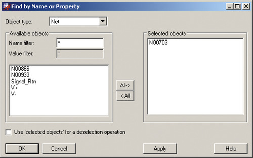 |
| Figure 9-46 Using the
Find filter to select specific nets. |
CROSS-HIGHLIGHTING BETWEEN CAPTURE AND PCB EDITOR
When working with large projects, it can be difficult to find specific nets or parts in your board design, or you might want to know where a particular trace belongs in the circuit. Cross-highlighting allows you to select a part in one application and see it highlighted in the other application.
To enable cross-highlighting, you need
Intertool Communication enabled in Capture and you have to be in highlight mode in PCB Editor.
To enableIntertool Communicationin Capture, select
Options → Preferences from the Capture menu bar. In the
Preferences dialog box (
Figure 9-47
), select the
Miscellaneous tab and check
Enable Intertool Communication. Click
OK.
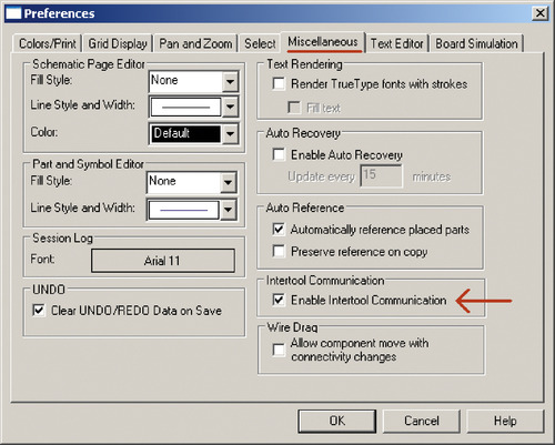 |
| Figure 9-47 Enable Intertool Communication in Capture. |
To enter the highlight mode in PCB Editor, click the
Highlight button,
 , on the PCB Editor toolbar (or select it from the
Display menu on the menu bar).
, on the PCB Editor toolbar (or select it from the
Display menu on the menu bar).
| Highlight button
|
Now if you select a net, a part, or a pin on a part in Capture, the corresponding object will be highlighted in PCB Editor. And, if you highlight a net, a part, or a pin on a part in PCB Editor, the corresponding object will be highlighted in Capture.
To dehighlight an object in Capture, simply click in a blank area in the schematic page, or click the
Dehighlight button,
 , in PCB Editor then click that object.
| Dehighlight button
|
To dehighlight an object in PCB Editor, you have to click the
Dehighlight button and select that object. Deselecting an object in Capture does not dehighlight the object in PCB Editor. Also, selecting the
Dehighlight button does not dehighlight all components; you have to click on each one individually or use the
Options filter tab to select certain objects (see
Figure 9-48
). Once you select the
Dehighlight button, cross-highlighting ceases. To restart cross-highlighting, you have to select the
Highlight button again.
 |
| Figure 9-48 Use the
Options pane to select types of objects to dehighlight. |
Note: If you reopened a board during an ECO process,
Intertool Communication may not work properly at first. If so, save the board, close it, then relaunch PCB Editor and reopen the board design normally (not through another ECO process).
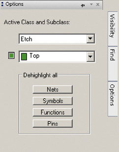
FINDING PARTS USING THE FIND FILTER PANE
Once the parts are in their relative positions, you can begin to carefully and precisely place the components. It is often a shuffle game at first, until you get a feel for the parts and the space you have to work with. Besides the cross-selection and cross-highlighting tools, another method for finding parts or nets is to use the
Find filter tab. To use the
Find filter to highlight a part, display the
Find pane (see
Figure 9-49
), select the object(s) you want to find (point 2), click the
More… button (point 3) to display the
Find by name or Property dialog box. In the list of components (or whatever you are looking for), select the item of interest (point 4) to move it to the
Selected objects window and click
Apply (point 5). The object will be centered in the screen and highlighted (as shown in the background of
Figure 9-49
).
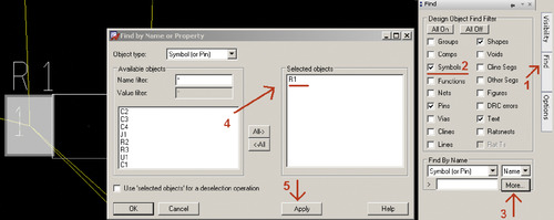 |
| Figure 9-49 Using the
Find filter to highlight a part. |
Once all the parts have been placed, your design might look something like that in
Figure 9-50
.
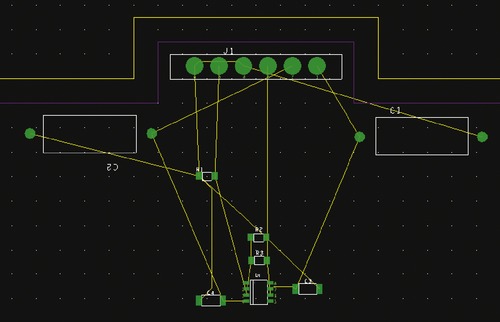 |
| Figure 9-50 The placed components. |
Some of the reference designators on the
Silkscreen layer might be upside down or in an undesirable location.
To rotate the reference designators, select the
Move button, check the
Text box in the
Find filter tab. Move your mouse to the
Options tab and select the desired angle from the list. Move your mouse back over to the board area and select the reference designator you want to rotate, right click and select
Rotate from the pop-up menu. Left click to place the text, right click and select
Done from the pop-up menu. Note: See also the Autosilk tool described in
Chapter 10
.
Design Rule Check and Status
The next steps in the design process are to define the layer stack-up and begin routing. Before we do that, though, it is a good idea to perform a design rule check (DRC) to check for any problems with the board and how the components are placed. By default the design rule checker is always on, so you do not usually have to specifically perform one unless it is out of date. There are two ways to update the DRC. The first way is to click the
Update DRC button,
 , on the toolbar (if that toolbar is displayed). The second way is to use the
Status dialog box.
, on the toolbar (if that toolbar is displayed). The second way is to use the
Status dialog box.
| Update DRC button
|
USING THE STATUS DIALOG BOX
To check for DRC errors through the Status tool, select
Display → Status from the menu bar. The
Status dialog box (see
Figure 9-51
) shows information about how many nets are routed, status of shapes, and if there are any DRC errors. If the
DRC Errors box is green, then there are no errors. If the
DRC Errors box is red, then there are errors in the design, but the box does not indicate what they are. If the
DRC Errors box is yellow, then either the DRC is out of date (click the
Update DRC to update it) or there are DRC
warnings. Warnings may be flagged rather than errors, depending on what the problem is and how the DRC parameters are set in the Constraint Manager (described shortly). To actually view what DRC errors are, you need to generate a DRC report.
 |
| Figure 9-51 The
Status dialog box. |
GENERATING DRC REPORTS
A DRC report is also used to find out the location of DRC errors and warnings as flagged by the Status tool.
To generate a DRC report, select
Tools → Quick reports → Design Rules Check Report from the menu bar. As shown in
Figure 9-52
, a DRC report tells you how many errors there are, where they are located, what type of errors they are, and who the offending parties are.
 |
| Figure 9-52 A DRC report. |
You can also generate a DRC report by selecting
Tools → Reports from the menu bar. A
Reports dialog box will be displayed as shown in
Figure 9-53
. From the
Reportsdialog box, you can select the type of report you want to see. It allows you to select additional options, such as generating multiple reports simultaneously and writing reports to files. To select a report, double click on the desired report in the
Available Reports section and then click the
Report button. A DRC report is the same with either method.
 |
| Figure 9-53 Selecting a report from the
Reports dialog box. |
You can create custom reports using the
Reports dialog box. An example of how to create a pick and place file is given in
Chapter 10
.
DRC ERROR MARKERS
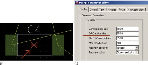
If you click on the DRC marker location in the DRC report, the error marker will be centered in your display. The DRC marker is bowtie shaped, as shown in
Figure 9-54
. You can change the size of DRC markers to make them easier to see.
To change the size of the DRC markers, select
Setup → Design Parameters from the menu bar. In the
Design Parameter Editor dialog box, select the
Display tab and change the marker size to the desired value. Click
Apply to apply the change and
OK to dismiss the dialog box.
 |
| Figure 9-54 A DRC marker (a) and its properties (b). |
You can find out additional information about a particular error with the
Show Element window.
To display additional information on a DRC marker, select the Show Element button,
 , on the toolbar, select
DRC Errors in the
Find filter tab, and then left click the DRC marker. A text box will be displayed that provides in-depth information about the error, as shown in
Figure 9-55
.
, on the toolbar, select
DRC Errors in the
Find filter tab, and then left click the DRC marker. A text box will be displayed that provides in-depth information about the error, as shown in
Figure 9-55
.
| Show Element button
|
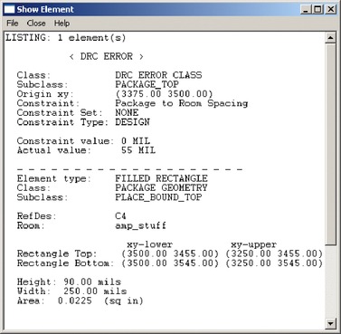 |
| Figure 9-55 Reviewing a DRC error with the Show Element tool. |
Once all DRC errors related to placement are corrected, the layer stack-up can be defined if it has not already been done.
Defining the Layer Stack-Up
The op amp used in this example requires a dual rail supply and at least one Ground plane. Two Routing layers also are needed. Therefore a minimum of five layers is required. Since most multilayer boards are made up of double-sided cores (and therefore usually have an even number of layers), we use the extra layer as an additional ground plane. The layers could be stacked up in several ways (see
Chapter 6
for other examples). The stack-up shown
Figure 9-56
is used in this example because it provides the opportunity to demonstrate two methods for defining Plane layers.
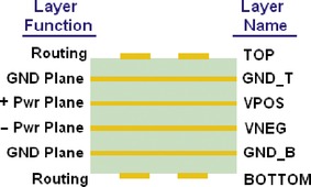 |
| Figure 9-56 Layer stack-up for Example 1. |
SETTING UP THE LAYOUT CROSS SECTION
Once you have the parts in place, the next step is to set up the layers. In this design we said that we needed six layers: two power planes, two ground pla-nes, and two routing layers.
First, let’s take an inventory of what we have.
To review or modify the layer stack-up, open the stack-up editor (
Layout Cross Section dialog box) by selecting the
Xsection button,
 , on the toolbar. The
Layout Cross Section dialog box is shown in
Figure 9-57
.
, on the toolbar. The
Layout Cross Section dialog box is shown in
Figure 9-57
.
| Xsection button
|
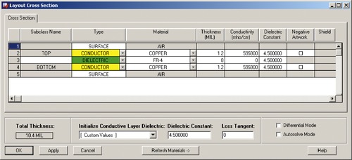 |
| Figure 9-57 The layer stack-up as shown in the
Layout Cross Section dialog box. |
The
Layout Cross Section dialog box lists the layers in the stack-up, their type, material properties, electrical properties, and image polarity.
By default the stack-up is defined by the outer surfaces (air), two Routing layers (top and bottom copper), and a dielectric layer (FR-4) between the copper layers. We now add four Plane layers and four Dielectric layers.
To add a Plane layer to the stack-up, right click on any one of the existing layers and select
Add Layer Above (or
Add Layer Below as appropriate) from the pop-up menu (see
Figure 9-58
). Do this eight times.
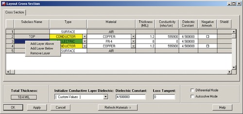 |
| Figure 9-58 Adding layers to the stack-up. |
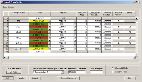
When you are finished, you will have eight dielectric layers. Convert every other layer to a Plane layer by selecting
Plane from the
Type list and
Negative from the
Negative Artwork column. The finished stack-up is shown in
Figure 9-59
. Click
Apply and then
OK. The
Shield property is related to analyses that are not enabled in the OrCAD version of PCB Editor, so it doesn’t matter if the option is checked or not.
 |
| Figure 9-59 The finished layer stack-up. |
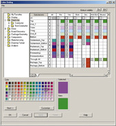
Now if you display the
Options pane, the new layers will be listed too. They all are given a default color, so you can customize your stack-up by changing the colors.
To change the color of a layer, select the
Colors button on the toolbar to display the
Colors dialog box. Select the
Stackup folder icon; the colors of all conductor and nonconductor layers will be shown. If you want to see only the conductor layers, select the
Conductor folder icon to narrow the view to just the Routing and Plane layers. Select a color from the pallet then select the box in the
Subclasses matrix to change its color.
Figure 9-60
shows an example of a custom color scheme for the stack-up. Generally it is a good idea to select light, neutral, shades for Plane layers, so that they are not too distracting, since they typically cover a large area. When you make changes to the color or visibility remember to click the
Apply button before clicking the
OK button and dismissing the color dialog box.
 |
| Figure 9-60 Setting custom colors for the stack-up. |
Once the stack-up is defined, the copper planes can be poured onto the proper layers.
Pouring Copper Planes
The two ways to pour a copper plane are to use the Setup Plane Outline tool or the Add Shape tool. We demonstrate both, beginning with the Add Shape tool. Afterward how padstacks are connected to the planes using the Setup Plane Outline tool will be demonstrated.
Before pouring the copper, set the etch grid to the proper resolution (100
mils is suggested for this exercise). As you are placing pick points, you can pan the view around by using the arrow keys on the keyboard and the mouse wheel if you have one (highly recommended).
POURING A COPPER PLANE USING THE
Setup → Outlines OPTION
To pour the copper, select the plane from the
Options menu (
Etch/GND_T, for example). Then select
Setup → Outlines → Plane Outline… from the menu bar, as shown in
Figure 9-61
. The
Plane Outline dialog box will be displayed (see
Figure 9-62
).
 |
| Figure 9-61 Starting a copper pour on a Plane layer. |
 |
| Figure 9-62 Drawing a plane area and assigning a net. |
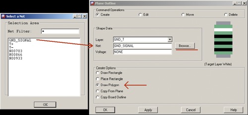
Using the
Plane Outline dialog box, connect the proper net to the layer by selecting the
Browse… button. In the
Select a Net dialog box, select the desired net and click
OK. If you are making a simple rectangle or box, you can select the Draw or
Place Rectangle radio buttons in the
Create Options section. Otherwise select the
Draw Polygon radio button (do not click
OK or
Apply yet).
Move your mouse pointer to the design area, left click and release to place the first vertex of the copper pour plane. If using the Polygon tool, place vertices (corners) to define the outline of the plane. Left click on the beginning point to complete the plane. If you are just drawing a rectangle, then left click at the corner opposite the starting point.
Note: In older versions of PCB Editor and newer versions that do not have the latest updates,
a copper area on a plane layer has to be dynamic copper. Filled rectangles and static shapes may not produce proper connectivity to component pins or may violate route keep-in and route keep-out areas. In newer versions with the latest updates, connectivity can be made with filled rectangles and static shapes. Verifying connectivity between pins and planes is discussed in the next section.
Before pouring copper areas on the next plane layers, check to see what type of shape was placed on the plane.
To determine what type of shape the copper is, hover your pointer over the plane; it should become highlighted and a data tips box should pop up with a description of the shape. If it does not, make sure that the
Shapes option is checked in the
Find filter pane. The poured copper will be one of three types and displayed as (1)
Filled Rectangle “Netname, Class/Subclass”, (2)
Shape, “Netname, Class/Subclass”, or (3)
Shape(auto-generated) “Netname, Class/Subclass”. For example if a copper pour area is dynamic copper on the Vpos layer and is connected +V net, the data tips pop-up box should say
Shape(auto-generated) “V+
, Etch/Vpos”.
If the copper pour object is the wrong type of shape, you can usually change it without having to delete and redraw it. To change a shape’s type, select
Shape → Change Shape Type from the menu. Check the
Options menu and make sure the
To dynamic copper option is selected. Left click the shape to select it then right click and select
Done from the pop-up menu. PCB Editor will display the warning
Converting from static to dynamic shapes results in the loss shape voids. –Continue? Click
Yes. The object should be converted to dynamic copper and all flashes, route keep-in, and route keep-out areas should be automatically updated. If problems persist, delete the object and redraw the copper pour area using the Add Shape tool, described next.
POURING A COPPER PLANE USING THE SHAPE ADD TOOL
To pour a copper plane using the Shape tool, select the target plane layer from the
Options pane (
Etch/Vpos, for example). Then click the
Shape Add (to place a polygon) or the
Shape Add Rect button (to place a rectangle). Go to the
Options pane again and make sure the shape fill type is
Dynamic copper. In the
Assign net name: area, click the
Browse… button to display the
Select a net dialog box, as shown in
Figure 9-63
. Left click the net to select it then click the
OK button to dismiss the dialog box. Left click in the work area to place each vertex of the plane outline. When you reach the last vertex, right click and select
Complete from the pop-up menu. The outline will be drawn but still highlighted with the editing handles (boxes) visible. You can modify the shape if necessary or right click and select
Done from the pop-up menu. Display the data tips box again to make sure the correct shape was drawn.
 |
| Figure 9-63 Drawing a copper pour shape and assigning a net. |
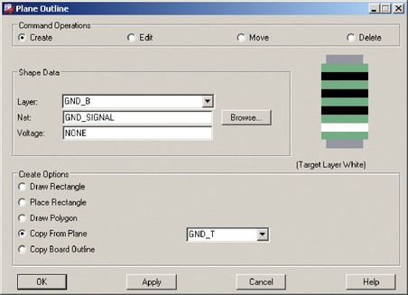
Once the first plane outline (copper pour area) is drawn, you can copy and paste it onto the other layers rather than drawing each one individually.
To copy a plane outline, start a new outline (
Setup → Outline → Plane Outlines… from the menu). As described previously, select the target layer and assign a net to the plane using the
Browse… button. In the
Create Options area, select the
Copy from Plane radio button, as shown in
Figure 9-64
. Select the existing plane from the list. At the command prompt it will say
select a plane to copy. Select the plane on its edge. This is done since there could be more than one plane on a layer and PCB Editor needs to know specifically which plane to copy. Click
OK when you have selected the plane. You should now have two Routing layers (top and bottom) and four Plane layers (two Ground and two Power planes). Again, make sure that the new copper pour areas are dynamic copper shapes, using the data tips box, and that connectivity is made from each plane to the correct pins as described next.
 |
| Figure 9-64 Drawing a new plane outline by copying an existing one. |
Verifying Connectivity between Pins and Planes
A padstack that connects to a plane usually does so through a thermal relief, while padstacks that are not connected to a plane are isolated from the plane with a clearance area around the padstack. Now that the planes are in place from the previous step, we need to make sure that connections to the plane and isolations from it are done properly. If you are using a version of PCB Editor that has had its libraries modified, then some of the following discussion may not apply. The original library that comes with PCB Editor contains some parts that lack the proper thermal reliefs and clearances assigned to the padstacks. If you zoom into J1 and turn off all the layers except for the top Ground plane, you should see one of the four views shown in
Figure 9-65
. If you see the bottom one, then the next section does not apply to you, so you can skip it and go to the section after that.
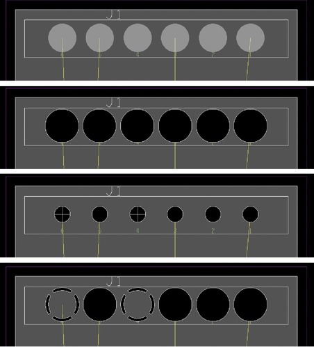 |
| Figure 9-65 Four possible views after placing a new plane outline. |
If you see the view shown at the top of
Figure 9-65
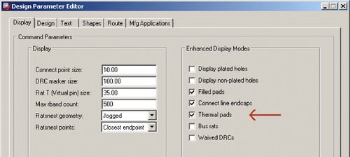
, you need to change the display options before you can see the thermal reliefs. To show thermal reliefs, select
Setup → Design Parameters from the menu. At the
Design Parameter Editor, select the
Display tab. In the
Enhanced Display Modes area, check the
Thermal pads option (see
Figure 9-66
). Click
Apply and then
OK.
 |
| Figure 9-66 Use the
Design Parameters Editor to show thermal reliefs. |
When viewing thermal pads is enabled in the
Design Parameters Editor, you should see either the third or fourth image in
Figure 9-65
. If you see the second image, then the plane outline is the wrong type. See the previous section to determine the type of outline and how to change it if it is wrong.
If you see the third image, then no thermal flashes have been assigned to the padstack. The next section explains how to modify your design to use the thermal reliefs and clearances.
If you see the bottom view, then your pads have been set up with thermal flashes and clearances, so you can skip down to the Defining Trace Width and Spacing Rules section.
ADDING THERMAL RELIEFS AND CLEARANCES TO PADSTACKS
To add the thermal reliefs to or change clearances on a padstack, you need to modify the padstack design using the Padstack Designer. You can modify just the padstack in the design or you can modify the padstack definition located in the symbols library. We will modify just the design padstack in this example.
To launch the Padstack Designer from PCB Editor, select
Tools → Padstack → Modify Design Padstack… from the menu bar. Move your pointer to connector J1, right click on pin 1 and select
Edit from the pop-up menu. The
Padstack Designer dialog box will be displayed. Select the
Layers tab as shown in
Figure 9-67
.
 |
| Figure 9-67 Use Padstack Designer to modify a padstack definition. |
On each of the layers, the thermal relief and clearance needs to be changed. Select a layer by clicking on it. Select
Flash from the list of thermal reliefs and either type
TR_180_150 in the flash name box or use the
Browse… button beside it to use the
Select flash symbol dialog box to choose from a list as shown in
Figure 9-68
.
 |
| Figure 9-68 Selecting a flash symbol for a pin. |
Note: To do this you must have the TR_180_150 flash symbol copied to the PCB Editor symbol folder with the other footprints or in the working allegro folder. You can copy the one in the
…share/pcb/examples folder in the OrCAD file path or from the Web site for this book.
Assign the flash symbol and change the clearance to 188 on each layer. Once the changes have been made, select
File → Update to Design… from the menu bar. Close the Padstack Designer to return to the board design. Right click and select
Done from the pop-up menu. You should see the thermal reliefs now (make sure you have the thermals box checked in the
Design Parameters dialog box).
Editing one pin actually edits all pins with the same name (even ones on different parts), so as you make each plane layer active, you should see the various clearances and thermals for the pins connected to that layer. If you want to change only one pin when there are many of that type of pin, select
Tools → Padstack → Modify Design Padstack… from the menu bar as before. Left click on the pin and in the
Options pane select the
Instance radio button. PCB Editor will automatically append a number to the name of the padstack to differentiate it from the others. Click the
Edit button at the bottom of the pane to display the Padstack Designer.
You will probably need to change the padstacks on part symbols C1 and C2, which use flash symbol TR_110_93. The remaining components in this design are surface mount and have no internal layers. And as we will see shortly, the vias are full contact type and do not use thermal reliefs.
Unless you modify the actual library parts, you will have to do this every time you start a new design and use the parts in the library. Instead of selecting the
Update design option, you can select the
Save to file option prior to closing the Padstack Designer. This saves a copy of the padstack (
name.pad) in the working directory. You can copy the padstack and put it in the symbols library, so that it can be used in other projects or you can select
Tools → Padstack → Modify Library Padstack… from the menu bar to modify it directly in the symbols library. You need to know the name of the padstack(s) that you want to modify to use this option. Over time many of the parts in the library will be modified and you should rarely have to do these modifications. However, you may want to back up the original library before you make a bunch of changes to it, and it is a good idea to make a backup of custom padstacks, flash symbols, and footprints that you develop as well.
Once the plane layers are properly set up you can fan out the surface-mount components to their respective Plane layers. To do this however, we need to assign or verify which via will be used for fan-outs and routing and that trace width and spacing requirements have been defined, as described in the next section.
Defining Trace Width and Spacing Rules
DETERMINING TRACE WIDTH
The trace width depends on three design considerations. The first consideration is the capabilities of your board manufacturer. The traces need to be wider than their minimum fabrication capability. The second consideration is the required current handling capability, and the third is the impedance. According to the data sheet, the short circuit output current for the 741
op amp is 64
mA. If we use a safety margin of, say, 100
mA and we are using a board with 1
oz copper, then per Eq. (6.17) in
Chapter 6
(or the graph from
Figure 6-38
), the minimum trace width is 1.3
mils for inner layers and 0.5
mils for outer layers. From
Table 6-8
in
Chapter 6
, you can see that, with 6-mil traces, you can run up to about 300
mA on inner traces and about 600
mA on outer traces. So the default value of 5
mils is adequate for most small-signal applications. However, the chosen width must also be manufacturable by your board house. Five mils is fairly narrow for many board houses, so we will change the widths.
For this example we specify that all signals be of very low frequency (<20
kHz) so that trace impedance is not a concern. An example of designing controlled-impedance transmission lines is given later in the digital design example (Example 4).
Trace width and spacing rules are set using the Constraint Manager.
To set trace width rules, open the Constraint Manager by clicking the
Cmgr button,
 , on the toolbar. Select the
Physical window and select the
All Layers icon in the
Net folder, as shown in
Figure 9-69
. The default minimum width for all nets is 5.00
mils and maximum is set at 0.00 (which means there is no maximum limit). Set the line widths to different values and note the differences when the board is routed later. Changes made in the Constraint Manager are effective immediately.
, on the toolbar. Select the
Physical window and select the
All Layers icon in the
Net folder, as shown in
Figure 9-69
. The default minimum width for all nets is 5.00
mils and maximum is set at 0.00 (which means there is no maximum limit). Set the line widths to different values and note the differences when the board is routed later. Changes made in the Constraint Manager are effective immediately.
| Cmgr button
|
 |
| Figure 9-69 Use the Constraint Manager to set trace width rules. |
ASSIGNING VIAS
Notice also in
Figure 9-69
that you can
specify particular vias for each net on the
Physical tab of the Constraint Manager. To select a different via, left click inside the cell for the via you want to change. In the
Edit Via List dialog box shown in
Figure 9-70
, select the via that you want to use on that net and remove unwanted via(s). Click
OK when your selection is complete. If you need a via that is not listed, you can make a custom via using the Padstack Designer, which is discussed in
Chapter 8
.
 |
| Figure 9-70 Use the
Edit Via List dialog box to establish the allowed vias. |
DETERMINING TRACE SPACING REQUIREMENTS
The op amp used in this example requires a dual rail supply, which can be up to ±15
V (and the input and output voltages must be between the rails). The greatest voltage difference possible between any two traces then is 30
V peak to peak, so the spacing between the traces must be able to support this. If we decide to play it safe and use the 31–50-V range and we plan on using a soldermask, then, using
Table 6-8
in
Chapter 6
, the route spacing should be greater than 4
mils on internal layers and greater than 5
mils on external layers. Again the selected spacing rules must fall within your board manufacturer’s capabilities also.
To set the spacing rules, select the
Spacing tab in the Constraint Manager. You can set spacing rules by layers or by nets.
To set the rules by layers, select the
All Layers icon in the
Spacing Constraint folder. In the
Objects column, you can click the+sign to expand and view the entire list of objects.
To set the rules by net, select the
All Layers icon in the
Net folder, as shown in
Figure 9-71
. To set specific rules (for example, line-to-line spacing, as shown), select the
Line icon under the
All Layers icon or the
Line tab at the bottom. In
Figure 9-71
,
Line To is circled in red at the top of the spreadsheet. If you select the
Pins icon (or tab), the words
Thru Pin To will be listed in place of
Line To. The spreadsheet is a matrix that gives you control over all the spacing rules.
 |
| Figure 9-71 Setting trace spacing rules in the Constraint Manager. |
Once all of the trace width and spacing rules are set we can begin routing fan-outs and traces.
Prerouting the Board
ROUTING FAN-OUTS FOR POWER AND GROUND
We want to fan out only power and ground, so we need to disable all the other nets. In particular we start with the Signal_RTN net on the GND layers. First we make the general nets invisible by turning on the No Rat property. To make nets invisible, open the
Constraint Manager and select the
Properties tab and select the
General Properties icon under the
Net folder.
To make a net invisible, select the
On option in the
No Rat column as shown in
Figure 9-72
.
To disable a net from being routed, select the
On option in the
No Route column. You can set a property on many nets simultaneously by dragging a box across the nets then setting the property. For this example make all nets invisible except for the SIGNAL_RTN net. For demonstration purposes we also want to prevent the power nets from being fanned out, so the No Route restriction is applied. Note that the signal nets will not be fanned out because we can control that by configuring the autorouter as shown next.
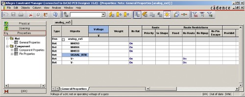 |
| Figure 9-72 Using
No Rat and
No Route to control net routability. |
Select
Route → Route Automatic… from the menu bar. Select the
Routing Passes tab in the
Automatic Router dialog box (see
Figure 9-73
). Select the
Fanout box and deselect the other boxes.
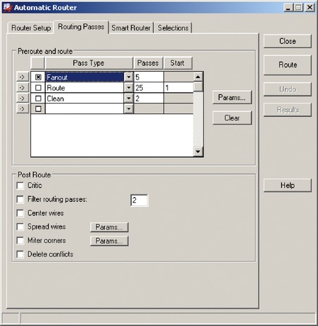 |
| Figure 9-73 Using the autorouter to perform fan-outs. |
Click the
Params… button to display the
SPECCTRA Automatic Router Parameters dialog box (see
Figure 9-74
). Here we can control what type of nets get fanned out, in what direction the fan-outs are routed, and how pins and vias are shared. Note that not all options are functional in the OrCAD version of PCB Editor. Under
Pin Types check the
Specified radio button and the
Power Nets box. This allows only nets assigned to Plane layers to be fanned out and, because the V+ and V− nets have a No-Route restriction (in Constraint Manager), only the SIGNAL_RTN net will be fanned out to the ground planes. Click
OK to dismiss the
Router Parameters dialog box. Click the
Route button on the
Automatic Router dialog box to begin the fan-out. Only the SIGNAL_RTN nets should be fanned out.
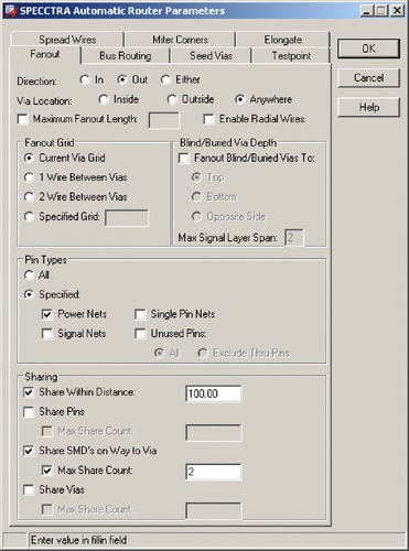 |
| Figure 9-74 Setting up fan-out options. |
To complete the fan-outs for the power nets, go back to the Constraint Manager and clear the no-route restriction; repeat the fan-out procedure for the V+ and V+ nets.
If you look closely at the vias used for the fan-outs (and routing by default), you will notice that they have no thermal reliefs to the Plane layers. If you want thermal reliefs for the vias, you can add them using same procedure as described previously to add thermals to the component pins. However, since leads or wires are typically not soldered into vias, many designers do not use thermal reliefs on routing and fan-out vias. There are arguments for both sides, but thermals are not used on the vias in this example.
MOVING AND DELETING FAN-OUTS
If the location of a fan-out is a problem, you can easily move it.
To move a fan-out, select the Slide tool,
 , left click on a via to select it. Move the pointer to where you want the via and left click to place the via.
| Slide tool
|
If for some reason you want to delete a fan-out and route it manually, you can do that too.
To rip up a fanout, select the Delete tool,
 , from the toolbar, select only the
Clines and
Cline Segs in the
Find filter, and select only
Clines and
Vias in the
Options tab. Double click the trace and via you want to rip up. Right click and select
Done from the pop-up menu when you are finished.
, from the toolbar, select only the
Clines and
Cline Segs in the
Find filter, and select only
Clines and
Vias in the
Options tab. Double click the trace and via you want to rip up. Right click and select
Done from the pop-up menu when you are finished.
| Delete tool
|
To manually redo a fanout, use the Add Connect tool,
 , to route a trace and fan-out via from the component pin (on the top or bottom layer) to a Plane layer. Make sure that the net is visible and does not have a No-Route restriction on it. Select the Add Connect tool, and left click the rat’s nest near the component’s pin. Left click at the location where you would like the via. Right click and select
Add Via from the pop-up menu. Right click and select
Done from the pop-up menu.
, to route a trace and fan-out via from the component pin (on the top or bottom layer) to a Plane layer. Make sure that the net is visible and does not have a No-Route restriction on it. Select the Add Connect tool, and left click the rat’s nest near the component’s pin. Left click at the location where you would like the via. Right click and select
Add Via from the pop-up menu. Right click and select
Done from the pop-up menu.
| Add Connect tool
|
Figure 9-75
(left) shows two shared via techniques, where the variation is a result of the via location.
Figure 9-75
(right) shows using individual vias instead of shared vias, where each part has its own vias. This approach makes routing a little easier, since it leaves an open path between the components on the top routing layer. As described in
Chapter 6
, there are arguments for all three types of fan-outs.
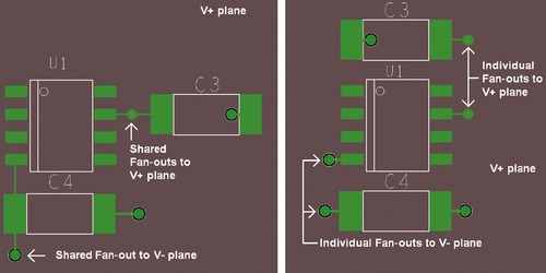 |
| Figure 9-75 Three fan-out methodologies. |
At this point it is a good idea to update the DRC. After all errors are fixed (there should be none), we can route the rest of the board.
Manually Routing Traces
Traces (clines) can be routed manually or by the autorouter. We begin by looking at manual routing.
TO BEGIN MANUALLY ROUTING TRACES
To manually route a trace, select the Add Connect tool,
 , left click on the desired trace, and left click again to place a vertex and route the trace. The default trace characteristics will be determined by the Constraint Manager. You can make changes to the trace as you are routing by using the
Options filter tab (see
Figure 9-76
), where you can change routing layers, line width, and other properties as shown in the figure.
, left click on the desired trace, and left click again to place a vertex and route the trace. The default trace characteristics will be determined by the Constraint Manager. You can make changes to the trace as you are routing by using the
Options filter tab (see
Figure 9-76
), where you can change routing layers, line width, and other properties as shown in the figure.
| Add Connect tool
|
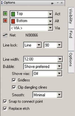 |
| Figure 9-76 Using the
Options tab to control manual routing properties. |
LOCKING (FIXING) TRACES
Once the fan-outs and specially routed traces are completed, you can lock (fix) them to prevent them from being inadvertently unrouted or shoved by the autorouter.
To fix traces, select the
Fix button,
 , from the toolbar and left click the desired trace.
To unlock (unfix) a trace, select the
Unfix button,
, from the toolbar and left click the desired trace.
To unlock (unfix) a trace, select the
Unfix button,
 , and left click a trace to unfix it. To find out if a trace is fixed or not, use the
Show Element button,
, and left click a trace to unfix it. To find out if a trace is fixed or not, use the
Show Element button,
 , and left click on a trace to find out the status. You can also use the Constraint Manager to fix traces (select the
Properties tab and set the
Route Restrictions properties).
, and left click on a trace to find out the status. You can also use the Constraint Manager to fix traces (select the
Properties tab and set the
Route Restrictions properties).
| Fix button
|
| Show Element button
|
| Unfix button
|
RUNNING THE AUTOROUTER
Once the fan-outs and manual routing tasks are completed, you can quickly route the rest of the board using the autorouter.
To start the autorouter, select
Route → Route Automatic… from the menu bar. As shown in
Figure 9-77
(
Route Setup tab,
Strategy options area), there are three ways to use the autorouter: (1) specify routing passes, (2) use the smart route, and (3) set up a
SPECCTRA (Allegro)
DO file. You use the
Route Setup tab on the
Automatic Router dialog box to select which method to use. Methods 1 and 2 are both easy to use, method 3 is not discussed here. The smart router has fewer options to set than the routing-passes method, but the routing-passes method gives you more control over the autorouter. Methods 1 and 2 are described next. Click the radio button for the method you want to use then click the corresponding tab to change the route settings for that method.
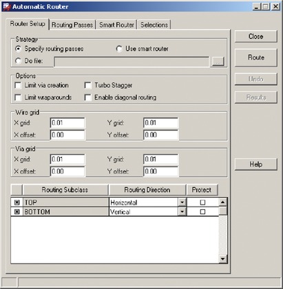 |
| Figure 9-77 Setting up the autorouter strategy and options. |
Use the
Smart Router tab to set up the autorouter for that method. As shown in
Figure 9-78
, you need to specify a minimum set of options, and they are pretty straightforward.
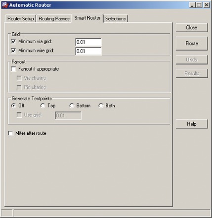 |
| Figure 9-78 Setting up the
Smart Router. |
With the routing-passes method, you have greater control over the routing process. In addition to the settings on the
Router Setup tab and the
Routing Passes tab, you also have access to the
Params… dialog box, as was shown during the fan-out description. Some of the features available in the routing-passes method are used in later examples. For this example just uncheck the
Fanout box (since we have already done that) and check the
Route and
Clean boxes. Click the
Route button to finish the board (
Figure 9-79
).
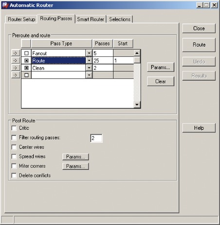 |
| Figure 9-79 Setting up the Routing Passes options. |
If your design is large and complicated, you can limit routing to specific sections of the board using the
Selection tab filter (see
Figure 9-80
). As shown, you can select (or restrict) specific nets for (from) routing. Using the
Selection tab in addition to the Constraint Manager. No-Route restrictions gives you extensive control over the autorouter.
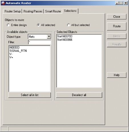 |
| Figure 9-80 Selecting which traces to route. |
..................Content has been hidden....................
You can't read the all page of ebook, please click here login for view all page.