Embedded DSP Software Design Using Multicore System-on-a-Chip (SoC) Architectures
Multicore System-on-a-Chip
Designing and building embedded systems is a difficult task, given the inherent scarcity of resources in embedded systems (processing power, memory, throughput, battery life, and cost). Various trade-offs are made between these resources when designing an embedded system. Modern embedded systems are using devices with multiple processing units manufactured on a single chip, creating a sort of multicore system-on-a-chip (SoC) can increase the processing power and throughput of the system while at the same time increasing the battery life and reducing the overall cost. One example of a DSP based SoC is shown in Figure 11.1. Multicore approaches keep hardware design in the low frequency range (each individual processor can run at a lower speed, which reduces overall power consumption as well as heat generation), offering significant price, performance, and flexibility (in software design and partitioning) over higher speed single-core designs.

There are several characteristics of SoC that we will discuss (reference 1). I will use an example processor to demonstrate these characteristics and how they are deployed in an existing SoC.
1. Customized to the application – Like embedded systems in general, SoC are customized to an application space. As an example, I will reference the video application space. A suitable block diagram showing the flow of an embedded video application space is shown in Figure 11.2. This system consists of input capture, real-time signal processing, and output display components. As a system there are multiple technologies associated with building a flexible system including analog formats, video converters, digital formats, and digital processing. An SoC processor will incorporate a system of components; processing elements, peripherals, memories, I/O, and so forth to implement a system such as that shown in Figure 11.2. An example of an SoC processor that implements a digital video system is shown in Figure 11.3. This processor consists of various components to input, process, and output digital video information. More about the details of this in a moment.


2. SoCs improve power/performance ratio – Large processors running at high frequencies consume more power, and are more expensive to cool. Several smaller processors running at a lower frequency can perform the same amount of work without consuming as much energy and power. In Figure 11.1, the ARM processor, the two DSPs, and the hardware accelerators can run a large signal processing application efficiently by properly partitioning the application across these four different processing elements.
3. Many apps require programmability – SoC contains multiple programmable processing elements. These are required for a number of reasons:
•New technology – Programmability supports upgradeability and changeability easier than nonprogrammable devices. For example, as new video codec technology is developed, the algorithms to support these new standards can be implemented on a programmable processing element easily. New features are also easier to add.
• Support for multiple standards and algorithms – Some digital video applications require support for multiple video standards, resolutions, and quality. Its easier to implement these on a programmable system.
• Full algorithm control – A programmable system provides the designer the ability to customize and/or optimize a specific algorithm as necessary which provides the application developer more control over differentiation of the application.
• Software reuse in future systems – By developing digital video software as components, these can be reuse/repackaged as building blocks for future systems as necessary.
4. Constraints such as real-time, power, cost – There are many constraints in real-time embedded systems. Many of these constraints are met by customizing to the application.
6. Special instructions – SoCs have special CPU instructions to speed up the application. As an example, the SoC in Figure 11.3 contains special instructions on the DSP to accelerate operations such as:
• 32-bit multiply instructions for extended precision computation
• Expanded arithmetic functions to support FFT and DCT algorithms
• Improve complex multiplications
• Double dot product instructions for improving throughput of FIR loops
• Parallel packing Instructions
• Enhanced Galois Field Multiply
Each of these instructions accelerate the processing of certain digital video algorithms. Of course, compiler support is necessary to schedule these instructions, so the tools become an important part of the entire system as well.
7. Extensible – Many SoCs are extensible in ways such as word size and cache size. Special tooling is also made available to analyze systems as these system parameters are changes.
8. Hardware acceleration – There are several benefits to using hardware acceleration in an SoC. The primary reason is better cost/performance ratio. Fast processors are costly. By partitioning into several smaller processing elements, cost can be reduced in the overall system. Smaller processing elements also consume less power and can actually be better at implementing real-time systems as the dedicated units can respond more efficiently to external events.
Hardware accelerators are useful in applications that have algorithmic functions that do not map to a CPU architecture well. For example, algorithms that require a lot of bit manipulation require a lot of registers. A traditional CPU register model may not be suited to efficiently execute these algorithms. A specialized hardware accelerator can b built that performs bit manipulation efficiently which sits beside the CPU and used by the CPU for bit manipulation operations. Highly responsive I/O operations are another area where a dedicated accelerator with an attached I/O peripheral will perform better. Finally, applications that are required to process streams of data, such as many wireless and multimedia applications, do not map well to the traditional CPU architecture, especially those that implement caching systems. Since each streaming data element may have a limited lifetime, processing will require the constant thrashing of cache for new data elements. A specialized hardware accelerator with special fetch logic can be implemented to provide dedicated support to these data streams.
Hardware acceleration is used on SoCs as a way to efficiently execute classes of algorithms. We mentioned in the chapter on power optimization, how the use of accelerators if possible can lower overall system power since these accelerators are customized to the class of processing and, therefore, perform these calculations very efficiently. The SoC in Figure 11.3 has hardware acceleration support. In particular, the video processing sub-system (VPSS) as well as the Video Acceleration block within the DSP subsystem are examples of hardware acceleration blocks used to efficiently process video algorithms. Figure 11.4 shows a block diagram of one of the VPSS. This hardware accelerator contains:

Figure 11.4 Block diagram of the video processing subsystem acceleration module of the SoC in Figure 11.3 (courtesy of Texas Instruments)
• CCDC (charge coupled device)
• Resizer (accepts data from the previewer or from external memory and resizes from ¼x to 4x)
And a back end module containing:
This VPSS processing element eases the overall DSP/ARM loading through hardware acceleration. An example application using the VPSS is shown in Figure 11.5.

Figure 11.5 A Video phone example using the VPSS acceleration module (courtesy of Texas Instruments)
9. Heterogeneous memory systems – Many SoC devices contain separate memories for the different processing elements. This provides a performance boost because of lower latencies on memory accesses, as well as lower power from reduced bus arbitration and switching.
This programmable coprocessor is optimized for imaging and video applications. Specifically, this accelerator is optimized to perform operations such as filtering, scaling, matrix multiplication, addition, subtraction, summing absolute differences, and other related computations.
Much of the computation is specified in the form of commands which operate on arrays of streaming data. A simple set of APIs can be used to make processing calls into this accelerator. In that sense, a single command can drive hundreds or thousands of cycles.
As discussed previously, accelerators are used to perform computations that do not map efficiently to a CPU. The accelerator in Figure 11.6 is an example of an accelerator that performs efficient operations using parallel computation. This accelerator has an 8-parallel multiply accumulate (MAC) engine which significantly accelerates classes of signal processing algorithms that requires this type of parallel computation. Examples include:
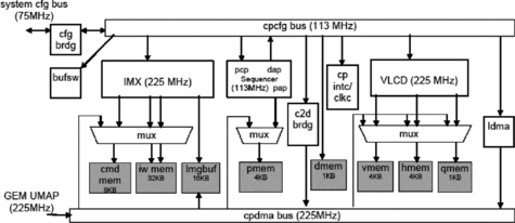
Figure 11.6 A hardware accelerator example; video and imaging coprocessor (courtesy of Texas Instruments)
• MPEG-1/2/4 encode and decode
• H.264 baseline profile decode
The variable length code/decode (VLCD) module in this accelerator supports the following fundamental operations very efficiently;
• Quantization and inverse quantization (Q/IQ)
• Variable length coding and decoding (VLC/VLD)
The design of this block is such that it operates on a macroblock of data at a time (max 6 8×8 blocks, 4:2:0 format). Before starting to encode or decode a bitstream, the proper registers and memory in the VLCD module must first be initialized by the application software.
This hardware accelerator also contains a block called a sequencer which is really just a 16-bit microprocessor targeted for simple control, address calculation, and loop control functions. This simple processing element offloads the sequential operations from the DSP. The application developer can program this sequencer to coordinate the operations among the other accelerator elements including the iMX, VLCD, System DMA, and the DSP. The sequencer code is compiled using a simple macro using support tools, and is linked with the DSP code to be later loaded by the CPU at run time.
One of the other driving factors for the development of SoC technology is the fact that there is an increasing demand for programmable performance. For many applications, performance requirements are increasing faster than the ability of a single CPU to keep pace. The allocation of performance, and thus response time, for complex realtime systems is often easier with multiple CPUs. And dedicated CPUs in peripherals or special accelerators can offload low-level functionality from a main CPU, allowing it to focus on higher-level functions.
Software Architecture for SoC
Software development for SoC involves partitioning the application among the various processing elements based on the most efficient computational model. This can require a lot of trial and error to establish the proper partitioning. At a high level the SoC partitioning algorithm is as follows:
• Place the state machine software (those algorithms that provide application control, sequencing, user interface control, event driven software, and so on) on a RISC processor such as an ARM.
• Place the signal processing software on the DSP, taking advantage of the application specific architecture that a DSP offers for signal processing functions.
• Place high rate, computationally intensive algorithms in hardware accelerators, if they exist and if they are customized to the specific algorithm of consideration.
As an example, consider the software partitioning shown in Figure 11.7. This SoC model contains a general-purpose processor (GPP), a DSP, and hardware acceleration. The GPP contains a chip support library which is a set of low level peripheral APIs that provide efficient access to the device peripherals, a general-purpose operating system, an algorithmic abstraction layer and a set of API for and application and user interface layer. The DSP contains a similar chip support library, a DSP centric kernel, a set of DSP specific algorithms and interfaces to higher level application software. The hardware accelerator contains a set of APIs for the programmer to access and some very specific algorithms mapped to the acceleration. The application programmer is responsible for the overall partitioning of the system and the mapping of the algorithms to the respective processing elements. Some vendors may provide a “black box” solution to one or more of these processing elements, including the DSP and the hardware accelerators. This provides another level of abstraction to the application developer who does not need to know the details of some of the underlying algorithms. Other system developers may want access to these low level algorithms, so there is normally flexibility in the programming model for these systems, depending on the amount of customization and tailoring required.

Communication in an SoC is primarily established by means of software. The communication interface between the DSP and the ARM in Figure 11.7, for example, is realized by defining memory locations in the DSP data space as registers. The ARM gains read/write access to these registers through a host interface. Both processors can asynchronously issue commands to each other, no one masters the other. The command sequence is purely sequential; the ARM cannot issue a new command unless the DSP has sent a “command complete” acknowledgement.
There exist two register pairs to establish the two-way asynchronous communication between ARM and DSP, one register pair is for the sending commands to ARM, and the other register pair is for the sending commands to DSP. Each register pair has:
• a command register, which is used pass commands to ARM or DSP;
• a command complete register, which is used to return the status of execution of the command;
• each command can pass up to 30 words of command parameters;
• also, each command execution can return up to 30 words of command return parameters.
An ARM to DSP command sequence is as follows:
• ARM writes a command to the command register
• ARM writes number of parameters to number register
• ARM writes command parameters into the command parameter space
• ARM issues a Nonmaskable interrupt to the DSP
• DSP reads the command parameters
• DSP clears the command register
• DSP writes result parameters into the result parameter space
The DSP to ARM command sequence is as follows:
• DSP writes command to command register
• DSP writes number of parameters to number register
• DSP writes command parameters into the command parameter space
• DSP issues an HINT interrupt to the DSP
• ARM reads the command parameters
• ARM clears the command register
• ARM writes result parameters into the result parameter space
Communication between the ARM and the DSP is usually accomplished using a set of communication APIs. Below is an example of a set of communication APIs between a general-purpose processor (in this case an ARM) and a DSP. The detailed software implementation for these APIs is given at the end of the chapter.
#define ARM_DSP_COMM_AREA_START_ADDR 0x80
Start DSP address for ARM-DSP.
#define ARM_DSP_COMM_AREA_END_ADDR 0xFF
#define ARM_DSP_DSPCR (ARM_DSP_COMM_AREA_START_ADDR)
ARM to DSP, parameters and command from ARM.
#define ARM_DSP_DSPCCR (ARM_DSP_COMM_AREA_START_ADDR+32)
ARM to DSP, return values and completion code from DSP.
#define ARM_DSP_ARMCR (ARM_DSP_COMM_AREA_START_ADDR+64)
DSP to ARM, parameters and command from DSP.
#define ARM_DSP_ARMCCR (ARM_DSP_COMM_AREA_START_ADDR+96)
DSP to ARM, return values and completion code from ARM.
#define DSP_CMD_MASK (Uint16)0x0FFF
#define DSP_CMD_COMPLETE (Uint16)0x4000
ARM-DSP command complete, from DSP.
#define DSP_CMD_OK (Uint16)0x0000
#define DSP_CMD_INVALID_CMD (Uint16)0x1000
#define DSP_CMD_INVALID_PARAM (Uint16)0x2000
Functions
STATUS ARMDSP_sendDspCmd (Uint16 cmd, Uint16 *cmdParams, Uint16 nParams)
Send command, parameters from ARM to DSP.
STATUS ARMDSP_getDspReply (Uint16 *status, Uint16 *retParams, Uint16 nParams)
Get command execution status, return parameters sent by DSP to ARM.
STATUS ARMDSP_getArmCmd (Uint16 *cmd, Uint16 *cmdParams, Uint16 nParams)
Get command, parameters sent by DSP to ARM.
STATUS ARMDSP_sendArmReply (Uint16 status, Uint16 *retParams, Uint16 nParams)
Send command execution status, return parameters from ARM to DSP.
SoC System Boot Sequence
Normally, the boot image for DSP is part of the ARM boot image. There could be many different boot images for the DSP for the different tasks DSP needs to execute. The sequence starts with the ARM downloading the image related to the specific task to be executed by the DSP. ARM resets then the DSP (via a control register) and then brings the DSP out of reset. At this stage the DSP begins execution at a pre-defined location, usually in ROM. The ROM code at this address initializes the DSP internal registers and places the DSP into an idle mode. At this point ARM downloads the DSP code by using a host port interface. After it completes downloading the DSP image, the ARM can send an interrupt to the DSP, which wakes it up from the idle mode, vectors to a start location and begins running the application code loaded by the ARM. The DSP boot sequence is given below:
• ARM resets DSP and then brings it out of reset.
• DSP gets out of reset and load its program counter (PC) register with a start address.
• The ROM code in this location branches the DSP to an initialization routine address.
• A DSP status register is initialized to move the vector table to a dedicated location, all the interrupts are disabled except for a dedicated unmaskable interrupt and the DSP is set to an mode.
• While DSP is in its mode, the ARM loads the DSP Program/Data memory with the DSP code/data.
• When the ARM finishes downloading the DSP code, it wakes up DSP from the mode by asserting an interrupt signal.
• The DSP then branches to a start address where the new interrupt vector table is located. The ARM should have loaded this location with at least a branch to the start code.
Tools Support for SoC
SoC, and heterogeneous processors in general, require more sophisticated tools support. A SoC may contain several programmable debuggable processing elements that require tools support for code generation, debug access and visibility, and real-time data analysis. A general model for this is shown in Figure 11.8. A SoC processor will have several processing elements such as an ARM and DSP. Each of these processing elements will require a development environment that includes mechanisms to extract, process, and display debug and instrumentation streams of data, mechanisms to peak and poke at memory and control execution of the programmable element, and tools to generate, link, and build executable images for the programmable elements.
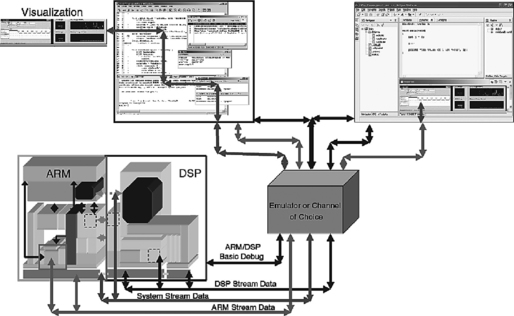
SoC tools environments also contain support for monitoring the detailed status of each of the processing elements. As shown in Figure 11.9, detailed status reporting and control of the processing elements in an Soc allows the developer to gain visibility into the execution profile of the system. Also, since power sensitive SoC devices may power down some or all of the device as the application executes, it is useful to also understand the power profile of the application. This can also be obtained using the proper analysis tools.

A Video Processing Example of SoC
Video processing is a good example of a commercial application requiring a system on a chip solution. Video processing applications are computationally intensive and demand a lot of MIPS to maintain the data throughput required for these applications. Some of the very compute-intensive algorithms in these applications include:
To perform a 30 frame per second MPEG-4 algorithm can take as much as 2500 MIPS depending on the resolution of the video.
The Audio channel processing is not as demanding but still requires enough overall MIPS to perform audio compression and decompression, equalization and sample rate conversion.
As these applications become even more complex and demanding (for example new compression technologies are still being invented), these SoC will need to support not just one but several different compression standards. SoCs for video applications include dedicated instruction set accelerators to improve performance. The SoC programming model and peripheral mix allows for the flexibility to support several formats of these standards efficiently.
For example the DM320 SoC processor in Figure 11.10 has an on chip SIMD engine (called iMX) dedicated to video processing. This hardware accelerator can perform the common video processing algorithms (Discrete Cosine Transform (DCT), IDCT, Motion Estimation, Motion Correlation to name a few)
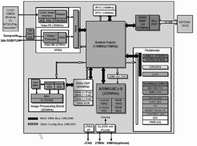
Figure 11.10 A SoC designed for video and image processing using a RISC device (ARM926) and a DSP (courtesy of Texas Instruments)
The VLCD (variable length coding/decoding) processor is built to support variable length encoding & decoding as well as quantization of standards such as JPEG, H.263, MPEG-1/2/4 video compression standards.
As you can see from the figure, an SoC solution contains appropriate acceleration mechanisms, specialized instruction sets, hardware co-processors, etc that provide efficient execution of the important algorithms in DSP applications. We discussed an example of video processing but you will find the same mechanisms supporting other applications such as wireless basestation and cellular handset.
The code listings below implement the ARM-side APIs that talk to the DSP Controller module that manages the ARM/DSP interface across the DSP’s Host Port Interface. These APIs are used to boot and reset the DSP and load the DSP code from the ARM, since the DSP can only execute code from internal memory that ARM loads.
static STATUS DSPC_hpiAddrValidate(Uint32 dspAddr, Uint8 read);
Reset the DSP, Resets the DSP by toggling the DRST bit of HPIB Control Register.
Generate an Interrupt to the DSP. Generates either INT0 or NMI interrupt to the DSP depending on which one is specified.
param intID DSP interrupt ID : INT0 - interrupt 0 NMI - NMI interrupt
eturn if success, c E_PASS, else error code
STATUS DSPC_strobeINT(DSP_INT_ID intID) {
Assert the hold signal to the DSP
Release the hold signal that was asserted to the DSP
Check if HOLD acknowledge signal received from DSP
return((DM_BOOL)(DSPC_FGET(HPIBSTAT, HOLDA) == 0 ? DM_TRUE : DM_
Enable/Disable byte swapping when transferring data over HPI interface
param enable Byte swap, DM_TRUE: enable, DM_FALSE: disable
STATUS DSPC_byteSwap(DM_BOOL enable) {
DSPC_FSET(HPIBCTL, EXCHG, ((enable == DM_TRUE) ? 1 : 0));
param enable HPI interface, DM_TRUE: enable, DM_FALSE: disable
STATUS DSPC_hpiEnable(DM_BOOL enable) {
DSPC_FSET(HPIBCTL, EXCHG, ((enable == DM_TRUE) ? 1 : 0));
Get HPI interface status register HPIBSTAT
eturn register HPIBSTAT (0x30602)
Write data from ARM address space to DSP address space
Memory map in DSP address space is as follows:
Address Address Access Description
0x60 0x7F R/W DSP specific memory area (32W)
0x80 0x7FFF R/W DSP on-chip RAM, mapped on
both program and data space (~32KW)
0x8000 0xBFFF R/W DSP on-chip RAM, mapped on
0x1C000 0x1FFFF R/W DSP on-chip RAM,
mapped on program space only (16KW)
param address Absolute address in ARM address space, must
param size Size of data to be written, in units of 16-
param dspAddr Absolute address in DSP address space, 0x0
eturn if success, c E_PASS, else error code
STATUS DSPC_writeData(Uint16 *address, Uint32 size, Uint32 dspAddr) {
if(DSPC_hpiAddrValidate(dspAddr, 0) != E_PASS)
hpiAddr=(Uint16*)HPI_DSP_START_ADDR;
if(((dspAddr >= 0x10000) && (dspAddr < 0x18000)) || (dspAddr >=
hpiAddr += (dspAddr - 0x10000);
}else if((dspAddr <= 0x0060) && (dspAddr > 0xC000)){
hpiAddr = (Uint16*)COP_SHARED_MEM_START_ADDR;
hpiAddr += (dspAddr − 0xC000);
Read data from DSP address space to ARM address space
Memory map in DSP address space is as follows:
Address Address Access Description
0x60 0x7F R/W DSP specific memory area (32W)
0x80 0x7FFF R/W DSP on-chip RAM, mapped on
0x8000 0xBFFF R/W DSP on-chip RAM, mapped on
0x1C000 0x1FFFF R/W DSP on-chip RAM, mapped on
param address Absolute address in ARM address space, must
param size Size of data to be read, in units of 16-bit
param dspAddr Absolute address in DSP address space, 0x0
eturn if success, c E_PASS, else error code
STATUS DSPC_readData(Uint16 *address, Uint32 size, Uint32 dspAddr) {
if(DSPC_hpiAddrValidate(dspAddr, 1) != E_PASS)
hpiAddr=(Uint16*)HPI_DSP_START_ADDR;
if(((dspAddr >= 0x10000) && (dspAddr < 0x18000)) || (dspAddr >=
hpiAddr += (dspAddr − 0]×10000);
}else if((dspAddr >= 0x0060) && (dspAddr < 0xC000)){
hpiAddr = (Uint16*)COP_SHARED_MEM_START_ADDR;
hpiAddr += (dspAddr − 0]xC000);
Similar to DSPC_writeData(), except that after writting it
verifies the contents written to the DSP memory
Memory map in DSP address space is as follows:
Address Address Access Description
0x60 0x7F R/W DSP specific memory area (32W)
0x80 0x7FFF R/W DSP on-chip RAM, mapped on
0x8000 0xBFFF R/W DSP on-chip RAM, mapped on
0x1C000 0x1FFFF R/W DSP on-chip RAM, mapped on
param address Absolute address in ARM address space, must
param size Size of data to be written, in units of 16-
param dspAddr Absolute address in DSP address space, 0x0
param retryCount Number of times to retry in case of failure
in writting data to DSP memory
eturn if success, c E_PASS, else error code
STATUS DSPC_writeDataVerify(Uint16 *address, Uint32 size, Uint32 dspAddr,
if(DSPC_hpiAddrValidate(dspAddr, 0) != E_PASS)
hpiAddr=(Uint16*)HPI_DSP_START_ADDR;
if(((dspAddr >= 0x10000) && (dspAddr < 0x18000)) || (dspAddr >=
hpiAddr += (dspAddr − 0]×10000);
}else if((dspAddr >= 0x0060) && (dspAddr < 0xC000)){
hpiAddr = (Uint16*)COP_SHARED_MEM_START_ADDR;
hpiAddr += (dspAddr − 0]xC000);
param pCode code to be dowloaded
STATUS DSPC_loadCode(const DSPCODESOURCE* pCode) {
if (pCode == NULL || pCode->size == 0)
// download the code to DSP memory
if(DSPC_writeDataVerify((Uint16 *)pCode->code, pCode->size, pCode-
static STATUS DSPC_hpiAddrValidate(Uint32 dspAddr, Uint8 read) {
// even if dspAddr <= 0x80 allow write
if(dspAddr >= 0x60 && dspAddr <= 0xFFFF)
if(dspAddr >= 0x10000 && dspAddr <= 0x17FFF)
if(dspAddr >= 0x1c000 && dspAddr <= 0x1FFFF)
Send command, parameters from ARM to DSP
This routine also triggers the NMI interrupt to DSP
param cmd command to be sent to DSP
param cmdParams pointer to paramters
param nParams number of parameters to be sent 0..30,
if c nParams < 30, then remaining ARM-DSP register set is filled with 0’s
eturn if success, c E_PASS, else error code
STATUS ARMDSP_sendDspCmd(Uint16 cmd, Uint16* cmdParams, Uint16 nParams) {
DSPC_writeData(&, 1, ARM_DSP_COMM_AREA_START_ADDR);
DSPC_writeData(nParams, 1, ARM_DSP_COMM_AREA_START_ADDR+1);
DSPC_writeData(cmdParams, nParams, ARM_DSP_COMM_AREA_START_ADDR+2);
Get command execution status, return parameters sent by DSP to
param status command status received from DSP
param retParams pointer to return paramters
param nParams number of parameters to be fetched from
ARM-DSP communication area, 0..30
eturn if success, c E_PASS, else error code
STATUS ARMDSP_getDspReply(Uint16* status, Uint16* retParams, Uint16 nParams
DSPC_readData(status, 1, ARM_DSP_COMM_AREA_START_ADDR+32);
DSPC_readData(retParams, nParams, ARM_DSP_COMM_AREA_START_ADDR+34);
Get command, parameters sent by DSP to ARM
param cmd command received from DSP
param cmdParams pointer to paramters
param nParams number of parameters to be fetched from
ARM-DSP communication area, 0..30
eturn if success, c E_PASS, else error code
STATUS ARMDSP_getArmCmd(Uint16* cmd, Uint16* cmdParams, Uint16 nParams) {
DSPC_readData(cmd, 1, ARM_DSP_COMM_AREA_START_ADDR+64);
DSPC_readData(cmdParams, nParams, ARM_DSP_COMM_AREA_START_ADDR+66);
Send command execution status, return parameters from ARM to DSP
This routine also triggers the NMI interrupt to DSP
param status command execution status to be sent to DSP
param retPrm pointer to return paramters
param nParams number of parameters to be sent 0..30,
if c nParams < 30, then remaining ARM-DSP register set is filled with 0’s
eturn if success, c E_PASS, else error code
STATUS ARMDSP_sendArmReply(Uint16 status, Uint16* retParams, Uint16 nParams
DSPC_writeData(&status, 1, ARM_DSP_COMM_AREA_START_ADDR+96);
DSPC_writeData(retParams, nParams, ARM_DSP_COMM_AREA_START_ADDR+98);
Clear ARM-DSP communication area
eturn if success, c E_PASS, else error code
memset((char*)nullArray, 0, 256);
if(DSPC_writeData(nullArray, 128, ARM_DSP_COMM_AREA_START_ADDR) !=
References
1. Multiprocessor systems-on-chips, by Ahmed jerraya, hannu tenhunen and Wayne Wolf. IEEE Computer. July 2005:36.
2. Embedded Software in Real-Time Signal Processing Systems: Design Technologies. Proceedings of the IEEE. 1997;85:3.
3. A Software/Hardware Co-design Methodology for Embedded Microprocessor Core Design. IEEE. 1999.
4. Component-Based Design Approach for Multicore SoCs. Copyright 2002. 2002. [ACM.].
5. A Customizable Embedded SoC Platform Architecture, IEEE IWSOC’04 <- International Workshop on System-on-Chip for Real-Time Applications.
6. How virtual prototypes aid SoC hardware design, Hellestrand, Graham. EEdesign.com. May 2004.
7. Panel Weighs Hardware, Software Design Options, Edwards, Chris. EETUK.com. Jun 2000.
8. Back to the Basics: Programmable SoCs, Zeidman, Bob. Embedded.com. July 2005.