
Cache Optimization in DSP and Embedded Systems
A cache is an area of high-speed memory linked directly to the embedded CPU. The embedded CPU can access information in the processor cache much more quickly than information stored in main memory. Frequently-used data is stored in the cache.
There are different types of caches but they all serve the same basic purpose. They store recently-used information in a place where it can be accessed very quickly. One common type of cache is a disk cache. This cache model stores information you have recently read from your hard disk in the computer’s RAM, or memory. Accessing RAM is much faster than reading data off the hard disk and therefore this can help you access common files or folders on your hard drive much faster. Another type of cache is a processor cache which stores information right next to the processor. This helps make the processing of common instructions much more efficient, and therefore speeding up computation time.
There has been historical difficulty in transferring data from external memory to the CPU in an efficient manner. This is important for the functional units in a processor as they should be kept busy in order to achieve high performance. However, the gap between memory speed and CPU speed is increasing rapidly. RISC or CISC architectures use a memory hierarchy in order to offset this increasing gap and high performance is achieved by using data locality.
Principle of locality
The principle of locality says a program will access a relatively small portion of overall address space at any point in time. When a program reads data from address N, it is likely that data from address N+1 is also read in the near future (spatial locality) and that the program reuses the recently read data several times (temporal locality). In this context, locality enables hierarchy. Speed is approximately that of the uppermost level. Overall cost and size is that of the lowermost level. A memory hierarchy from the top to bottom contains registers, different levels of cache, main memory, and disk space, respectively (Figure C.1)

There are two types of memories available today. Dynamic Random Acces Memory (DRAM) is used for main memory and is cheap but slow. Static Random Access Memory (SRAM) is more expensive, consumes more energy, and is faster.
Vendors use a limited amount of SRAM memory as a high-speed cache buffered between the processors and main memory to store the data from the main memory currently in use. Cache is used to hide memory latency which is how quickly a memory can respond to a read or write request. This cache can’t be very big (no room on chip), but must be fast. Modern chips can have a lot of cache, including multiple levels of cache:
A general comparison of memory types and speed is shown in Figure C.2. Code that uses cache efficiently show higher performance. The most efficient way of using cache is through a block algorithm which is described later.

Caching schemes
There are various caching schemes used to improve overall processor performance. Compiler and hardware techniques attempt to look ahead to ensure the cache is full of useful (not stale) information. Cache is refreshed at long intervals using several techniques. Random replacement will throw out any current block at random. First-in/first-out (FIFO) replace the information that has been in memory the longest. Least recently used (LRU) replace the block that was last referenced the furthest in the past. If a request is in the cache it’s a cache hit. The higher hit rate the better performance. A request that is not in the cache is a miss.
As an example, if a memory reference were satisfied from L1 cache 70% of the time, L2 cache 20% of the time, L3 cache 5% of the time and main memory 5% of the time, the average memory performance would be:
(0.7 * 4) + (0.2 * 5) + (0.05 * 30) + (0.05 * 220) = 16.30 ns
Caches work well when a program accesses the memory sequentially;
sum = sum = sum + a(i) ! accesses successive
The performance of the following code is not good!
sum = sum = sum + a(i) ! accesses large data structure
The diagram in Figure C.3 (the model on the left) shows a flat memory system architecture. Both CPU and internal memory run at 300 MHz. A memory access penalty will only occur when CPU accesses external memory. There are no memory stalls that will occur for accesses to internal memory. But what happens if we increase the CPU clock to 600 MHz? We would experience wait-states! We also would need a 600 MHz memory. Unfortunately, today’s available memory technology is not able to keep up with increasing processor speeds. A same size internal memory running at 600 MHz would be far too expensive. Leaving it at 300 MHz is not possible as well, since this would effectively reduce the CPU clock to 300 MHz as well (Imagine in a kernel with memory access every EP, every EP will suffer 1 cycle stall, effectively doubling the cycle count and thus canceling out the double clock speed).

The solution is to use a memory hierarchy, with a fast, but small and expensive memory close to the CPU that can be accessed without stalls. Further away from the CPU the memories become larger but slower. The memory levels closest to the CPU typically act as a cache for the lower level memories.
So, how does a cache work in principle and why does it speed-up memory access time?
Let’s look at the access pattern of a FIR filter, a 6-tap FIR filter in this case. The required computations are shown here. To compute an output we have to read in 6 data samples (we also need 6 filter coefficients, but these can be neglected here since it’s relatively little data compared to the sample data) from an input data buffer x[]. The numbers denote in which order the samples are accessed in memory. When the first access is made, the cache controller fetches the data for the address accessed and also the data for a certain number of the following addresses into cache. This range of addresses is called a cache line. [Fetching the line from the slower memory is likely cause a few CPU stall cycles.] The motivation for this behavior is that accesses are spatially local, that is if a memory location was accessed, a neighboring location will be accessed soon as well. And it is true for our FIR filter, the next 5 samples are required as well. This time all accesses will go into fast cache instead of slow lower level memory[, without causing any stall cycles]. Accesses that go to neighboring memory locations are called spatially local.
Let’s see what happens if we calculate the next output. The access pattern is shown in Figure C.4. Five of the samples are being re-used and only one sample is new, but all of them are already held in cache. Also no CPU stalls occur. This illustrates the principle of temporal locality: the same data that was used in the previous step is being used again for processing;

• Spatial locality – If memory location was accessed, neighboring location will be accessed as well.
• Temporal locality – If memory location was accessed, it will be accessed soon again [look-up table]
Cache builds on the fact that data accesses are spatially and temporally local. Accesses to a slower lower level memory are minimal, and the majority of accesses can be serviced at CPU speed from the high level cache memory. As an example:
N = 1024 output data samples, 16-tap filter: 1024 * 16 / 4 = 4096 cycles
Stall cycles to bring 2048 byte into cache: about 100 cycles (2.5 cycles per 64-byte line), about 2.4%.
In other words, we have to pay with 100 cycles more, and in return we are getting double the execution speed, that’s still in the end 1.95x speed-up!
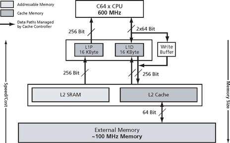
The C64x memory architecture (Figure C.5) consists of a 2-level internal cache-based memory architecture plus external memory. Level 1 cache is split into program (L1P) and data (L1D) cache, each 16 KBytes. Level 1 memory can be accessed by the CPU without stalls. Level 1 caches cannot be turned off. Level 2 memory is configurable and can be split into L2 SRAM (addressable on-chip memory) and L2 Cache that caches external memory addresses. On a TI C6416 DSP for instance, the size of L2 is 1 MByte, but only one access every two cycles can be serviced. Finally, external memory can be up to 2 GBytes, the speed depends on the memory technology used but is typically around 100 MHz. All caches (red) and data paths shown are automatically managed by the cache controller.
Mapping of addressable memory to L1P
First. let’s have a look at how direct-mapped caches work. We will use the L1P of C64x as an example for a direct-mapped cache. Shown in Figure C.6 are the addressable memory (e.g., L2 SRAM), the L1P cache memory and the L1P cache control logic. L1P Cache is 16 KBytes large and consists of 512 32-byte lines. Each line always maps to the same fixed addresses in memory. For instance addresses 0x0 to 0x19 (32 bytes) will always be cached in line 0, addresses 3FE0h to 3FFFh will always be cached in line 511. Then, since we exhausted the capacity of the cache, addresses 4000h to 4019h map to line 0 again, and so forth. Note here that one line contains exactly one instruction fetch packet.

Access, invalid state of cache, tag/set/offset
Now let’s see what happens if the CPU accesses address location 20h. Assume that cache has been completely invalidated, meaning that no line contains cached data.The valid state of a line is indicated by the valid bit. A valid bit of 0 means that the corresponding cache line is invalid, i.e., doesn’t contain cached data. So, when the CPU makes a request to read address 20h, the cache controller takes the address and splits it up into three portions: the offset, the set and the tag portion. The set portion tells the controller to which set the address maps to (in case of direct caches a set is equivalent to a line). For the address 20h the set portion is 1. The controller then checks the tag and the valid bit. Since we assumed that the valid bit is 0, the controller registers a miss, i.e., the requested address is not contained in cache.
Miss, line allocation
A miss means that the line containing the requested address will be allocated in cache. That is the controller fetches the line (20h-39h) from memory and stores the data in set 1. The tag portion of the address is stored in the tag RAM and the valid bit is set to 1. The fetched data is also forwarded to the CPU and the access is complete. Why we need to store a tag portion becomes clear when we access address 20h again.
Re-access same address
Now, let’s assume some time later we access address 20h again. Again the cache controller takes the address and splits it up into the three portions. The set portion determines the set. The stored tag portion will be now compared against the tag portion of the address requested. This is comparison is necessary since multiple lines in memory map to the same set. If we had accessed address 4020h which also maps to the same set, but the tag portions would be different, thus the access would have been a miss. In this case the tag comparison is positive and also the valid bit is 1, thus the controller will register a hit and forward the data in the cache line to the CPU. The access is completed.
At this point it is useful to remind ourselves what the purpose of a cache is. The purpose of a cache is to reduce the average memory access time. For each miss we have to pay a penalty to get (allocate) a line of data from memory into cache. So, to get the highest returns for what we “paid” for, we have to re-use (read and/or write accesses) this line as much as possible before it is replaced with another line. Re-using the line but accessing different locations within that line improves the spatial locality of accesses, re-using the same locations of a line improves the temporal locality of accesses. This is by the way the fundamental strategy of optimizing memory accesses for cache performance.
The key is here re-using the line before it gets replaced. Typically the term eviction is used in this context: The line is evicted (from cache). What happens if a line is evicted, but then is accessed again? The access misses and the line must first be brought into cache again. Therefore, it is important to avoid eviction as long as possible. So, to avoid evictions we must know what causes an eviction. Eviction is caused by conflicts, i.e., a memory location is accessed that maps to the same set as a memory location that was accessed earlier. The newly accessed location will cause the previous line held at that set to be evicted and to be allocated in its place. Another access to the previous line will now cause a miss.
This is referred to as a conflict miss, a miss that occurred because the line was evicted due to a conflict before it was re-used. It is further distinguished whether the conflict occurred because the capacity of the cache was exhausted or not. If the capacity was exhausted then the miss is referred to as a capacity miss. Identifying the cause of a miss, helps to choose the appropriate measure for avoiding the miss. If we have conflict misses that means the data accessed fits into cache, but lines get evicted due to conflicts.
In this case we may want to change the memory layout so that the data accessed is located at addresses in memory that do not conflict (i.e., map to the same set) in cache. Alternatively, from a hardware design point of view, we can create sets that can hold two or more lines. Thus, two lines from memory that map to the same set can both be allocated in cache without having one evict the other. How this works will see shortly on the next slide.
If we have capacity misses, we may want to reduce the amount of data we are operating on at a time. Alternatively, from a hardware design point of view, we could increase the capacity of the cache.
There is a third category of misses, the compulsory misses or also called first reference misses. They occur when the data is brought in cache for the first time. As opposed to the other two misses above, they cannot be avoided, thus they are compulsory.
An extension of direct-mapped caches are so-called set-associative caches (Figure C.7). For instance the C6x’s L1D is a 2-way set associative cache, 16 KBytes capacity and has 64-byte lines. Its function shall now be explained. The difference to a direct-mapped cache is that here one set consists of two lines, one line in way 0 and one line in way 1, i.e., one line in memory can be allocated in either of the two lines. For this purpose the cache memory is split into 2 ways, each way consisting of 8 KBytes.

Hits and misses are determined the same as in a direct-mapped cache, except that now two tag comparisons are necessary, one for each way, to determine in which way the requested data is kept. If there’s a hit in way 0, the data of the line in way 0 is accessed, if there’s a hit in way 1 the data of the line in way 1 is accessed.
If both ways miss, the data needs to be allocated from memory. In which way the data gets allocated is determined by the LRU bit. An LRU bit exists for each set. The LRU bit can be thought of as a switch: if it is 0 the line is allocated in way 0, if it is 1 the line gets allocated in way 1. The state of the LRU bit changes whenever an access (read or write) is made to a cache line: If the line in way 0 is accessed the LRU bit switches to 1 (causing the line in way 1 to be replaced) and if line 1 is accessed the LRU bit switches to 0. This has the effect that always the Least-recently-used (or accessed) line in a set will be replaced, or in other words the LRU bit switches to the opposite way of the way that was accessed, as to “protect” the most-recently-used line from replacement. Note that the LRU bit is only consulted on a miss, but its status is updated every time a line in the set is accessed regardless whether it was a hit or a miss, a read or a write.
As the L1P, the L1D is a read-allocated cache, that is new data is allocated from memory on a read miss only. On a write miss, the data goes through a write buffer to memory bypassing L1D cache. On a write hit the data is written to the cache but not immediately to memory. This type of cache is referred to as write-back cache, since data that was modified by a CPU write access is written back to memory at a later time. So, when is the data written back?
First of all we need to know which line was modified and needs to be written back to lower level memory. For this purpose every cache line has a dirty bit (D) associated to it. It’s called dirty because it tells us if the corresponding line was modified. Initially the dirty bit will be zero. As soon as the CPU writes to a line, the corresponding dirty bit will be set to 1. So again, when is a dirty line written back? It’s written back on a read miss that will cause new data to be allocated in a dirty line. Let’s assume the line in set 0, way 0 was written to by the CPU, and the LRU bit indicates that way 0 is to be replaced on the next miss. If the CPU now makes a read access to a memory location that maps to set 0, the current dirty data contained in the line is first written back to memory, then the new data is allocated in that line. A write-back can also be initiated by the program by sending a write back command to the cache controller. This is however, not usually required.
Now let’s start looking at cache coherence. So, what do we mean by cache coherence? If multiple devices, such as the CPU or peripherals, share the same cacheable memory region, cache and memory can become incoherent. Let’s assume the following system. Suppose the CPU accesses a memory location which gets subsequently allocated in cache (1). Later, a peripheral is writing data to this same location which is meant to be read and processed by the CPU (2). However, since this memory location is kept in cache, the memory access hits in cache and the CPU will read the old data instead of the new one (3). The same problem occurs if the CPU writes to a memory location that is cached, and the data is to be written out by a peripheral. The data only gets updated in cache but not in memory from where the peripheral will read the data. The cache and the memory is said to be “incoherent.”
How is this problem addressed? Typically a cache controller is used that implements a cache coherence protocol that keeps cache and memory coherent. Let’s see how this is addressed in the C6x memory system.
A good strategy for optimizing cache performance is to proceed in a top-down fashion (Figure C.8), starting on application level, moving to procedural level, and if necessary considering optimizations on algorithmic level. The optimization methods for application level tend to be straightforward to implement and typically have a high impact on overall performance improvement. If necessary, fine tuning can then be performed using lower level optimization methods. Hence the structure of this chapter reflects the order in which one may want to address the optimizations.

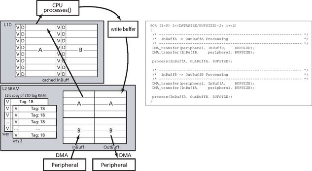
To illustrate the coherency protocols, let’s assume a peripheral is writing data to an input buffer located in L2 SRAM, (Figure C.9) then the CPU reads the data processes it and writes it back to an output buffer, from which the data is written to another peripheral. The data is transferred by the DMA controller. We’ll first consider a DMA write, i.e., peripheral fills input buffer with data, the next slide will then show the DMA read, i.e., data in the output buffer is read out to a peripheral.

Figure C.9 DMA Write operations. This is the recommended use: Stream data to L2SRAM not external memory. (courtesy of Texas Instruments)
1. The peripheral requests a write access to line 1 (lines mapped form L1D to L2SRAM) in L2 SRAM. Normally the data would be committed to memory, but not here.
2. The L2 Cache controller checks it’s local copy of L1D tag ram if the line that was just requested to be written to is cached in L1D by checking the valid bit and the tag. If the line is not cached in L1D no further action needs to be taken and the data is written to memory.
3. If the line is cached in L1D, the L2 controller sends a SNOOP-INVALIDATE command to L1D. This sets the valid bit of the corresponding line to zero, i.e., invalidates the line. If the line is dirty it is written back to L2 SRAM, then the new data from the peripheral is written.
4. The next time the CPU accesses this memory location, the access will miss in L1D and the line containing the new data written by the peripheral is allocated in L1D and read by the CPU. If the line had not been invalidated, the CPU would have read the “old” value that was cached in L1D.
Aside, the L2 controller sends an INVALIDATE command to L1P. This is necessary in case we want to load program code. No data needs to be written back in this case since data in L1P is never modified.
Having described how a DMA write and read to L2 SRAM works, we will see next how everything plays together in the example of a typical double-buffering scheme (Figure C.10). Let’s assume we want read in data from one peripheral, process it, and write it out through another peripheral—a structure of a typical signal processing application. The idea is that while the CPU is processing data accessing one set of buffers (e.g., InBuff A and OutBuff A), the peripherals are writing/reading data using the other set of buffers such that the DMA data transfer occurs in parallel with CPU processing.
Let’s start off assuming that InBuffA has been filled by the peripheral.
1. Transfer is started to fill InBuffB.
2. CPU is processing data in InBuffA. The lines of InBuffA are allocated in L1D. Data is processed by CPU and written through the write buffer (remember that L1D is read-allocated) to OutBuffA.
3. Buffers are then switched, and CPU is reading InBuffB and writing OutBuffB. InBuffB gets cached in L1D.
4. At the same time the peripheral fills InBuffA with new data. The L2 cache controller takes automatically care of invalidating the corresponding lines in L1D through Snoop-Invalidates so that the CPU will allocated the line again from L2 SRAM with the new data rather reading the cached line containing the old data.
5. Also, the other peripheral reads OutBuffA. However, since this buffer is not cached in L1D no Snoops are necessary here.
It’s always a good idea to make the buffers fit into a multiple of cache lines, in order to get the highest return (in terms of cached data) for every cache miss.
Here’s a code example how such a double buffering scheme could be realized. It uses CSL calls to DAT_copy and DAT_wait.
This is recommended over DMA double buffering in external memory.
Now let’s look at the same double buffering scenario (Figure C.11), but now with the buffers located in external memory. Since the cache controller does not automatically maintain coherence, it is the responsibility of the programmer to maintain coherence manually. Again, the CPU reads in data from a peripheral processes it and writes it out to another peripheral via DMA. But now the data is additionally passed through L2 Cache.
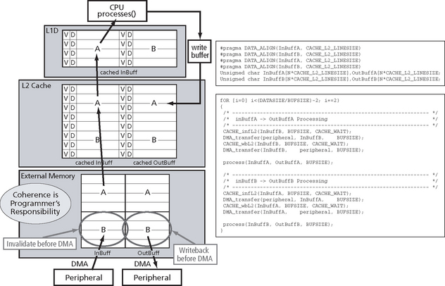
Let’s assume that transfers already have occurred and that both InBuff and OutBuff are cached in L2 Cache and also that InBuff is cached in L1D. Further let’s assume that CPU has completed consuming inBuffB and filled OutBuffB and is now about to start processing the A buffers. Before we call the process function, we want to initiate the transfers that bring in new data into the InBuffB and commits the data in OutBuffB just written by the CPU to the peripheral.
We already know from the previous example what the L2 cache controller did to keep L2 SRAM coherent with L1D. We have to do exactly the same here to ensure that external memory is kept coherent with L2 Cache and L2 Cache with L1D. In the previous example, whenever data was written to an input buffer, the cache controller would invalidate the corresponding line in the cache. Similarly, here we have to invalidate all the lines in L2 Cache AND in L1D that map to the external memory input buffer before we initiate the transfer (or after the transfer is completed). This way the CPU will re-allocated these lines from external memory next time the input buffer is read, rather than accessing the previous data that would still be in cache if we hadn’t invalidated. How can we invalidate the input buffer in cache?
Again the Chip Support Library (CSL) provides a set of routines that allow the programmer to initiate those cache operations. In this case we use CACHE_control(CACHE_L2, CACHE_INV, InBuffB, BUFSIZE); before the transfer starts. We need to specify the start address of the buffer in external memory and its number of bytes.
Similarly, before OutBuffB is transferred to the peripheral, the data first has to be written back from L2 Cache to external memory. This is done by issuing a CACHE_control(CACHE_L2, CACHE_WB, OutBuffB, BUFSIZE);. Again, this is necessary since the CPU writes data only to the cached version if OutBuffB.
Before we move on to the next slide which shows a summary of the available L2 cache operations: To prevent unexpected incoherence problems, it is important that we align all buffers at a L2 cache line size make their size a multiple of cache lines. It’s also a good idea to place the buffers contiguously in memory to prevent evictions.
I used the double buffering examples to show how and when to use cache coherence operations. Now, when in general do I need to use them?
Only if CPU and DMA controller share a cacheable region of external memory. By share we mean the CPU reads data written by the DMA and vice versa. Only in this case I need to maintain coherence with external memory manually.
The safest rule is to issue a Global Writeback-Invalidate before any DMA transfer to or from external memory. However, the disadvantage here is that we’ll probably operate on cache lines unnecessarily and get a relatively large cycle count overhead.
A more targeted approach is more efficient. First, we need to only operate on blocks of memory that we know are used as a shared buffer. Then we can also distinguish between the following three scenarios: The first two are familiar, we used them for our double buffering example. (1) If the DMA reads data written by the CPU, we need to use a L2 Writeback before the DMA starts, (2) If the DMA writes data that is to be read by the CPU, then we need to invalidate before the DMA starts. Then, a third case, the DMA may modify data that was written by the CPU that is consequently to be read back by the CPU. This is the case if the CPU initializes the memory first (e.g. sets it to zero) before a peripheral or else writes to the buffer. In this case we first need to commit the initialization data to external memory and then invalidate the buffer. This can be achieved with the Writeback-Invalidate command (On the C611/6711 an invalidate operation is not available. Instead a Writeback-Invalidate operation is used.)
When to use cache coherence control operations
The CPU and DMA share a cacheable region in external memory. The safest approach is to use writeback-invalidate all cache before any DMA transfer to/from external memory. The disadvantage is a large overhead for the operation. Overhead can be reduced by only operating on buffers used for DMA and distinguish between three possible scenarios shown in Figure C.12.

A good strategy for optimizing cache performance is to proceed in a top-down fashion, starting on application level, moving to procedural level, and if necessary considering optimizations on algorithmic level. The optimization methods for application level tend to be straightforward to implement and typically have a high impact on overall performance improvement. If necessary, fine tuning can then be performed using lower level optimization methods. Hence the structure of this chapter reflects the order in which one may want to address the optimizations.
Application level optimizations
There are various application level optimizations that can be performed in or to improve cache performance.
For signal processing code, the control and data flow of DSP processing are well understood and more careful optimization possible. Use the DMA for streaming data into on-chip memory to achieve the best performance. On-chip memory is closer to the CPU, and therefore latency is reduced. Cache coherence may be automatically maintained as well. Use L2 cache for rapid-prototyping applications but watch out for cache coherence related issues.
For general-purpose code, the techniques are a little different. General-purpose code has a lot of straight-line code and conditional branching. There is not much parallelism, and execution largely unpredictable In these situations, use L2 cache as much as possible.
Some general techniques to reduce the number of cache misses include maximizing the cache line re-use. Access all memory locations within a cached line The same memory locations within a cached line should be re-used as often as possible. Also avoid eviction of a line as long as it is being re-used. There are a few ways to do this;
Optimization techniques for cache-based systems
Before we can begin to discuss techniques to improve cache performance, we need to understand the different scenarios that may exist in relation to the cache and our software application. There are three main scenarios we need to be concerned about:
Scenario 1 – All data/code of the working set fits into cache. There are no capacity misses in this scenario by definition, but conflict misses do occur. In this situation, the goal is to eliminate the conflict misses through contiguous allocation.
Scenario 2 – The data set is larger than cache. In this scenario, no capacity misses occur because data is not reused. The data is contiguously allocated, but conflict misses occur. In this situation, the goal is to eliminate the conflict misses by interleaving sets.
Scenario 3 – The data set is larger than cache. In this scenario, capacity misses occur because data is reused. Conflict misses will also occur. In this situation, the goal is to eliminate the capacity and conflict misses by splitting up the working set
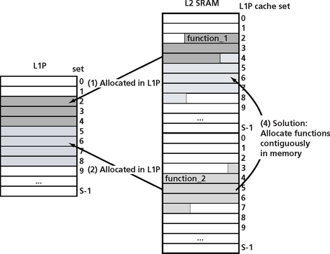
Scenario 1
The main goal for scenario 1 is to allocate function contiguously in memory. Figure C.13a shows two functions allocated in memory in overlapping cache lines. When these functions are read into the cache, because of the conflict in memory mapping of the two functions, the cache will be trashed as each of these functions is called (C.13b and c). A solution to this problem is to allocate these functions contiguously in memory as shown in Figure C.13d.


Scenario 2
Scenario 2 is the situation where the data set is larger than cache. No capacity misses occur in this situation because data is not reused. Data in memory is contiguously allocated but conflict misses occur. In this situation, the goal is to eliminate conflict misses by interleaving sets. Thrashing occurs if arrays are multiple of the size of one way. As an example consider Arrays w[], x[] and h[] map to the same sets in Figure C.15. This will cause misses and reduced performance. By simply adding a pad word, the offset for array h is now different from the other arrays and gets mapped into a different way in the cache. This improves overall performance.
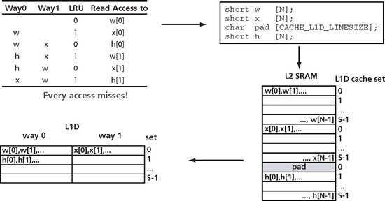
Figure C.14a shows an example of a set of variables being declared in an order that causes an inefficient mapping onto the architecture of a two-way set associative cache. A simple rearrangement of these declarations will result in a more efficient mapping into the two-way set associative cache and eliminate potential thrashing (Figure C.14b).

Scenario 3
Scenario 3 occurs when the data set is larger than the cache. Capacity misses occur because data is reused and conflict misses can occur as well. In this situation, we must eliminate the capacity and conflict misses by splitting up the working set. Consider the example in Figure C14.b where the arrays exceed cache capacity. We can solve this with a technique called blocking. Cache blocking is a technique to optimally structure application data blocks in such a way that they fit into a cache memory block. This is a method of controlling data cache locality, which in turn improves performance. I’ll show an algorithm to do this in a moment.

Before we consider the different cases, let’s consider the concept of processing chains.
Often the output of one algorithms forms the input of the next algorithm. This is shown in Figure C.17. An input buffer is read by func1 and writes its results to an temporary buffer which is used as input to func2. Func2 then writes its output to an output buffer. If we can keep tmp_buf allocated in L1D, then func2 will not see any read misses. The data is written to L1D and read from L1D, avoiding any data fetches from L2 memory!

So, read misses will only for the first function in the processing chain. All following functions can operate …
As another example, consider Figure C.18. There is a Read miss only for the first function in the chain. All following functions can operate directly on cached buffers: In this situation there is no cache overhead! The last function writes through the write buffer.
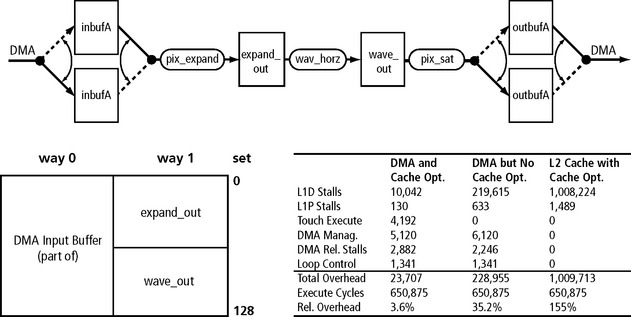
We have to keep the effects of processing chains in mind when we benchmark algorithms and applications. In this example the first function is a FIR filter which is followed by a dot product. The table below shows cycle count numbers for these algorithms. The execute cycles are shown, which are raw CPU execution cycles, below that L1D stalls that are predominately caused by L1D misses, and L1P stalls caused by L1P misses. The cycle counts are split up into 1st and 2nd iteration.
You see for the FIR filter the 1st and 2nd L1D stalls are about the same because we read new data from L2 SRAM, i.e., compulsory misses. On the other hand, once the temp buffer is allocated in L1D there are NO misses for the iterations after the 1st for dot prod (provided we have performed some optimization which I will describe in the next slides). We see in the 1st iteration we had 719 stalls (again compulsory misses) and in the 2nd we have only 6. Ideally this is 0, but we may get a few misses caused by stack accesses on function calls etc. The 719 stalls mean an overhead of 148%. This seems very large, but it’s really only for the first iteration. If you run the processing loop only 4 times, the combined overhead is only 1.9%!
So, when you benchmark an algorithm on a cache-based memory architecture you have to keep this in mind and consider the algorithm in the context how you use it in the application.
What happens if FIR and DOTPROD are reversed (Figure C.19)? The overhead would be higher, but not by much, it would be 2.5%. They key is having a algorithm that does a high amount of processing compared to the number of memory accesses, or has high amount of data re-use.

Interpretation of cache overhead benchmarks
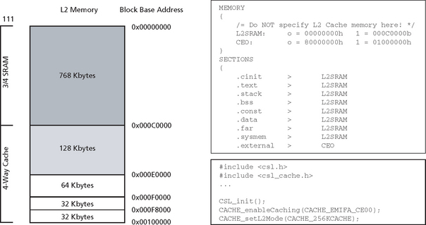
Now, let’s look at how to use and configure cache correctly. Whereas Level 1 cache cannot be switched off, L2 Cache can be configured in various sizes. The diagram on the left shows what configurations are possible. L2 Cache can be switched off, set to 32 KBytes, 64, 128 or 256 Kbytes. After reset L2 Cache is switched off. The rest is L2 SRAM which always starts at address 0x0. Let’s say we want to use 256K of L2 as cache. First of all we need to make sure that no data or code is being linked into the L2SRAM portion to be used as cache. Figure C.20 is an example of how an appropriate linker command file could look like. L2 SRAM runs starts at 0 and is hex C0000 bytes large, which is 768K, then Cache starts at C0000 and is hex 40000, which is 256Kbytes in decimal. The last memory is external memory. We make sure nothing is linked into it by NOT declaring it under the MEMORY directive. In the program we need to call this sequence of CSL commands to enable caching of external memory locations into L2. The first command initializes the CSL, then we enable caching of the external memory space CE00 which corresponds to the first 16MB in external memory. Finally, we set L2 Cache to 256K. That’s it.
Software transformation for cache optimization
There are various compiler optimizations that will improve cache performance. There are both instruction and data optimization opportunities using an optimizing compiler. An example of an instruction optimization is the reordering of procedures that reduce the cache thrashing that may occur. Reordering procedures can be done by first profiling the application and then using changes in the link control file to reorder these procedures.
The compiler may also perform several types of data optimizations including:
As an example of the compiler merging arrays, consider the array declarations below:
Restructuring the arrays as shown below will improve cache performance by improving spatial locality.
As an example of a loop interchange, consider the code snippet below:
z[ k ][ j ] = 10 * z[ k ][ j ];
By interchanging the second and third nested loops, we move to more of a sequential access instead of a stride of 100 words which will improve spatial locality.
z[ k ][ j ] = 10 * z[ k ][ j ];
As mentioned earlier, cache blocking is a technique to optimally structure application data blocks in such a way that they fit into a cache memory block. This is a method of controlling data cache locality which in turn improves performance. This can be done in the application or, in some cases, by using the compiler. The technique breaks large arrays of data into smaller blocks that can be repeat ably accessed during processing. Many video and image processing algorithms have inherent structures that allow them to be operated on this way. How much performance gains are available with this technique depend on the cache size, the data block size, and some other factors including how often the cached data can be accessed before being replaced. As an example, consider the snippet of code below:
A[i, j, k] = A[i, j, k] + B[i, k, j]
by changing this to a blocking structure like the one shown below, we can get maximum use of a data block while it is in cache before moving on to the next block. In this example, the cache block size is 20. The goal is to read in a block of data into the cache and perform the maximum amount of processing while the data is in the cache before moving on to the next block. In this case, there are 20 elements of array A and 20 elements of array B in the cache at the same time.
A[i, j, k] = A[i, j, k] + B[i, k, j]
Loop distribution is an optimization technique that attempts to split a large loop into smaller ones. These smaller loops not only increase the chance to be pipelined or vectorized by the compiler, but also increase the chance for the loop to fit into a cache in its entirety. This prevents the cache from trashing as the loop executes and improves performance. The code snippet below shows a for loop with a number of function calls inside the loop. By slitting up the loops,
*** code snippet before loop distribution
Application level cache optimizations
There are also some application-level optimizations that the developer should be aware of that will improve overall application performance. The optimizations will vary depending on whether the application is signal processing software of control code software. For signal processing software, the control and data flow of DSP processing are well understood. We can therefore perform more careful optimizations. One specific technique to improve performance is to use the DMA for streaming data into on-chip memory to achieve best performance. On-chip memory is closer to the CPU, and therefore the latency is reduced. Cache coherence may be automatically maintained by using this on chip memory. L2 cache should also be used for rapid-prototyping applications (but watch out for potential cache coherence issues!).
General-purpose DSP software is characterized by straight-line code and a lot of conditional branching. There is not much parallelism in this software and the execution s largely unpredictable. This is when the developer should configure the DSP to use L2 cache, if available.
Techniques overview
In summary, the DSP developer should consider the following cache optimizations for embedded DSP applications;
Figure C.21 is an example of a visual mapping of cache hits and misses over time. Both hits and misses form patterns when viewed visually that can alert the viewer to cache performance problems. Reordering data and program placement as well as using the other techniques we have been discussing will help eliminate some of these miss patterns.

Figure C.21 Cache Analysis lets you determine how the placement of your code in memory is impacting code execution
I would like to thank Oliver Sohm for his significant contributions to this appendix.