The Target
“What is the use of a book,” thought Alice, “without pictures or conversations?”
Lewis Carroll
Alice’s Adventures in Wonderland (1865)
The intention of this book is to show how to build embedded systems where the FPGA is the central computing device. The goal is not to teach how to design and fabricate an FPGA or show how to develop computer-aided design (CAD) tools for FPGA devices. Nonetheless, to meet the complex performance metrics described in the previous chapter, a good system designer has to understand how the programmable logic devices are manufactured, their basic electrical characteristics, and their general architectures. Unfortunately, the 10,000-meter view of FPGA devices of the first chapter is insufficient. Certain underlying details of FPGA technology are needed to understand what the software tools are doing when they transform a hardware description into a configuration. Although high-level synthesis tools have made huge strides over the years, basic knowledge of the target device almost always leads to more efficient designs.
The learning objectives of this chapter include:
• a short review of CMOS transistors and their central role as the building blocks of digital circuits.
• a brief discussion of programmable logic devices that have paved the way for modern FPGAs.
• the specifics of the FPGA, their low-level components, and those that are used to distinguish Platform FPGAs. This is a more detailed description than found in Chapter 1.
• a brief overview of hardware description languages; a useful tool to aid in complex digital circuit design.
• a description of the process of transforming a hardware description of the desired circuit into a stream of bits suitable to configure the FPGA device.
The examples used throughout this chapter were purposely chosen for their simplicity and brevity to help the reader quickly establish (or refresh) a foundation of knowledge to build upon in the remaining chapters.
2.1 CMOS Transistor
Because digital circuits, such as FPGAs, rely on CMOS transistors, being aware of their construct and, more specifically, their functionality can help aid the designer in making better overall design decisions. For example, power consumption is emphasized within this section to encourage readers to think about how their designs will behave based on these CMOS principles. The long-term result can be a more power-efficient design, a welcome addition to any embedded systems designs.
The details we do include are related to what an FPGA developer needs to know to make design decisions. First we cover the CMOS transistor. The intention is not to try to cover everything related to electronic circuits or even transistors. In fact, we rely on the reader already having taken at least one course in electronic circuits. We try to cover transistors with enough detail to act as a refresher or to help those less familiar with the material. As already stated, we are not setting out to design FPGAs, we aim to use them, and as such we should be familiar with their constructs. We then cover the progression from transistors to the programmable logic device, the precursor in many ways to the FPGA. Finally, we dwell into great detail regarding FPGAs.
Transistors have several distinct modes that make them useful in a variety of applications. However, here we simplify them to just one role: a voltage-controlled switch. The most common transistor in digital circuits is in the form of a Metal Oxide Semiconductor Field Effect Transistor (MOSFET). The MOSFET is created from two-dimensional regions in a slab of silicon substrate. The regions are constructed to have either an excess of positive or an excess of negative charge. A layer of silicon dioxide is placed over the substrate to insulate it from a metal layer placed above the silicon dioxide. An n-channel MOSFET transistor (or NMOS for short) is illustrated in Figure 2.1 with (a) a cut-away view of the silicon substrate and (b) the NMOS transistor’s schematic symbol. There are three electrical terminals on this transistor: source, drain, and gate.
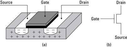
Figure 2.1 (a) An NMOS transistor in silicon substrate and (b) a schematic of an NMOS transistor.
As silicon is a semiconductor, the gate can be used to control whether current flows from the drain to the source. For an NMOS transistor, if the voltage difference between the gate and the source is close to 0, then current is able to flow from the drain to the source. But if the voltage difference is significant, say 5 volts, then the transistor is in “cut-off” mode. In cut-off mode it behaves like an open switch and current cannot flow from the drain to the source. Using schematic symbols, this circuit is shown in Figure 2.3. Note that the input is a voltage on the gate and the output is a voltage on the conductor connected to the drain.
With a low voltage producing current and a high voltage producing no current, this can be considered a form of an inverter (a Boolean NOT gate), and without much work the reader will recognize the NAND, NOR, and AND gates illustrated in Figure 2.2. At first glance, we now have what is necessary to build digital circuits from these basic gates. However, there are a number of problems with these circuits. The most important is power consumption. When the voltage drops over an electric component, potential energy is converted into heat. So whenever the output of Figure 2.3 is 0, current is flowing and the resistor is generating heat. (To a small degree, the transistor is, too.) It turns out that this use of power is unacceptable in practice.
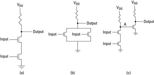
Figure 2.2 An NMOS (a) NAND gate, (b) NOR gate, and (c) AND gate.
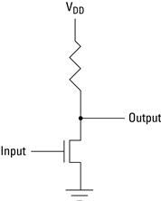
Figure 2.3 Schematic symbol of an NMOS inverter.
To address the power problem we consider the opposite of the n-channel transistor, the p-channel (or PMOS) transistor. PMOS rearranges the areas on the substrate so that regions that had an excess of negative charge now have an excess of positive charge and vice versa, shown in Figure 2.4. However, the PMOS inverter draws the most power when its output is high (because current is flowing and there is a voltage drop over the resistor). The PMOS unfortunately presents the same problem as the NMOS, only at the opposite time.
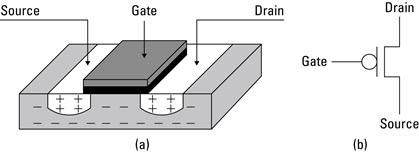
Figure 2.4 (a) A PMOS transistor in silicon substrate and (b) a schematic of a PMOS transistor.
We can get the best of both worlds if we combine a PMOS transistor with an NMOS transistor such that in the steady state, no appreciable current is flowing. The Complementary MOS (CMOS) transistor combines a simple CMOS NAND circuit and is illustrated in Figure 2.5. It also leads to an important rule of thumb: the greatest amount of energy in a design is consumed when a CMOS gate is changing state. In steady state, no (appreciable) current is flowing. However, when the inputs start to change and the MOSFET transistors have not completely switched on or off, current flows and power is dissipated.
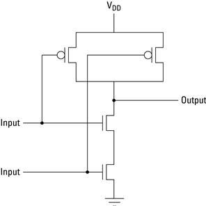
Figure 2.5 A simple CMOS NAND circuit.
2.2 Programmable Logic Devices
The transistors described in the last section are fixed at manufacture. The p- and n-type areas on the substrate, the silicon dioxide insulator, and metal layer(s) are created from masks. Once the chip is fabricated, those positions are fixed and, by extension, the transistor functionality is fixed, which leads to the question: how can devices be built that can be configured after manufacture/fabrication? To answer this, we need to build up a structure that is capable of implementing arbitrary combinational circuits, a storage cell (memory), and a mechanism to connect these resources.
The first programmable logic devices were organized around the sum-of-products formulation of a Boolean function. These devices, called Programmable Logic Arrays (PLAs), had an array of multi-input AND gates and an array of multi-input OR gates. The organization is shown in Figure 2.6. (Typically, the inputs ![]() ,
, ![]() , and
, and ![]() would also be inverted, and, in this case, six-input AND gates would be used.) To configure this device, all of the unwanted inputs to the AND gates are broken and all of the unwanted inputs to the OR gates are broken. However, for manufacturing reasons, this approach fell out of favor. The PLA can be simplified by hardwiring some AND gate outputs to specific OR gates. This constrains some inputs to use dedicated gates, but the PLA manufacturer compensates for this by increasing the number of gates. The PLA device is programmed by breaking unwanted connections at the inputs to the AND and OR gates.
would also be inverted, and, in this case, six-input AND gates would be used.) To configure this device, all of the unwanted inputs to the AND gates are broken and all of the unwanted inputs to the OR gates are broken. However, for manufacturing reasons, this approach fell out of favor. The PLA can be simplified by hardwiring some AND gate outputs to specific OR gates. This constrains some inputs to use dedicated gates, but the PLA manufacturer compensates for this by increasing the number of gates. The PLA device is programmed by breaking unwanted connections at the inputs to the AND and OR gates.
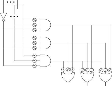
Figure 2.6 PLA device organization.
To these PLA structures, several programmable logic companies have introduced memory elements, such as D-type flip-flops. In this case they added a MUX and a D-Type Flip-Flop to the output of the OR gates. Hence, the output of the function can either be stored on a rising clock edge or the signal can bypass the flip-flop as illustrated in Figure 2.7. Connected to the outputs of the OR gates, this structure allows a designer to create state machines on programmable logic devices.
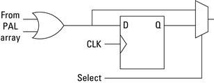
Figure 2.7 Adding storage to a PLA logic cell.
The final intermediate step in the progression from PLAs to FPGAs was the introduction of Complex Programmable Logic Devices (CPLDs). These devices start with a PLA block (with a storage element). These blocks are then replicated multiple times on a single Integrated Chip. A configurable routing network allows the different PLA blocks to be connected to one another and the outside pins. (The routing network is similar to those found on an FPGA, which is described next.)
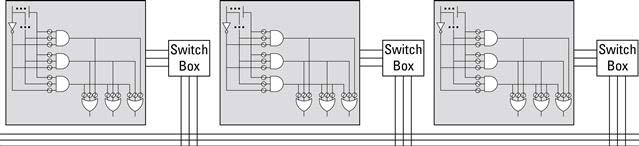
Figure 2.8 Simple CPLD device organization example.
2.3 Field-Programmable Gate Array
A modern FPGA consists of a 2-D array of programmable logic blocks, fixed-function blocks, and routing resources implemented in the CMOS technology. Along the perimeter of the FPGA are special logic blocks connected to external package I/O pins. Logic blocks consist of multiple logic cells, while logic cells contain function generators and storage elements. These general terms are discussed in more detail throughout this chapter. In Section 2.A specific details regarding the Xilinx Virtex 5 FPGA device constructs are given.
2.3.1 Function Generators
The programmable logic devices described thus far use actual gates implemented with CMOS transistors directly in the silicon to generate the desired functionality. FPGA devices are fundamentally different in that they use function generators to implement Boolean logic functionality rather than physical gates.
For example, suppose we want to implement the Boolean function:
![]()
Using a 3-input function generator, we first create the eight-row Boolean truth table for this function (as shown in Figure 2.9a). For each input the truth table represents what the output of the Boolean function will be. If each of the function’s output bits were stored into individual static memory (such as SRAM) cells and connected as inputs to an ![]() multiplexer (MUX), the three inputs (x,y,z) would be the select lines for the MUX. The result is commonly what is known as a look-up table (LUT).
multiplexer (MUX), the three inputs (x,y,z) would be the select lines for the MUX. The result is commonly what is known as a look-up table (LUT).
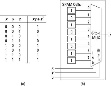
Figure 2.9 Three-input function generator in (a) truth table and (b) look-up table form.
We can draw the basic 3-input LUT circuit (Figure 2.9b) taking care to label the inputs 0 through 7 and identify the most significant select bit (MSB) and least significant select bit (LSB). The last step is to assign ![]() ,
, ![]() , and
, and ![]() to the select bits and fill in the SRAM cells with the corresponding entries in the truth table. As drawn, when
to the select bits and fill in the SRAM cells with the corresponding entries in the truth table. As drawn, when ![]() ,
, ![]() , and
, and ![]() are 0,0,0 then the bottom SRAM cell is selected, so ’1’ is stored there. When
are 0,0,0 then the bottom SRAM cell is selected, so ’1’ is stored there. When ![]() ,
, ![]() , and
, and ![]() are
are ![]() the second from the bottom SRAM cell is selected, so ’0’ is stored there. This continues through
the second from the bottom SRAM cell is selected, so ’0’ is stored there. This continues through ![]() where ’1’ is stored at the top SRAM cell.
where ’1’ is stored at the top SRAM cell.
This example illustrates, at a basic level, the process of mapping Boolean logic to FPGAs. Soon, we will discuss in more detail how to map more meaningful logic to the FPGA fabric. One additional important lesson to learn from this example is that unlike a digital circuit implemented within logic gates, the propagation delay from a LUT is fixed. This means, regardless of the complexity of the Boolean circuit, if it fits within a single LUT, the propagation delay remains the same. This is also true for circuits spanning multiple LUTs, but instead the delay depends on the number of LUTs and additional circuitry necessary to implement the larger function. More on that topic later.
To generalize the aforementioned example, the basic ![]() -input function generator consists of a
-input function generator consists of a ![]() -to-1 multiplexer (MUX) and
-to-1 multiplexer (MUX) and ![]() SRAM (static random access memory) cells. By convention, a 3-LUT is a 3-input function generator. The 3-input structure is shown for demonstration purposes, although 4-LUTs and 6-LUTs are more common in today’s components.
SRAM (static random access memory) cells. By convention, a 3-LUT is a 3-input function generator. The 3-input structure is shown for demonstration purposes, although 4-LUTs and 6-LUTs are more common in today’s components.
To implement a function with more inputs than would fit in a single LUT, multiple LUTs are used. The function can be decomposed into subfunctions of a subset of the inputs, each subfunction is assigned to one LUT, and all of the LUTs are combined (via routing resources) to form the whole function. There are some dedicated routing resources to connect neighboring LUTs with minimal delay to support low propagation delays.
An important observation is that SRAM cells are volatile; if power is removed the value is lost. As a result, we need to learn how to set the SRAM cell’s value. This process, called configuring (or programming), could be handled by creating an address decoder and sequentially writing the desired values into each cell. However, the number of SRAM cells in a modern FPGA is enormous and random access is rarely required. Instead, the configuration data are streamed in bit by bit. The SRAM cells are chained together such that, in program mode, the data out line of one SRAM cell is connected to the data in line with another SRAM cell. If there are ![]() cells, then the configuration is shifted into place after
cells, then the configuration is shifted into place after ![]() cycles. Some FPGA devices also support wider, byte-by-byte transfers as well to support parallel transfers for faster programming.
cycles. Some FPGA devices also support wider, byte-by-byte transfers as well to support parallel transfers for faster programming.
2.3.2 Storage Elements
While function generators provide the fundamental building block for combinational circuits, additional components within the FPGA provide a wealth of functionality. As in a PLA block, D-type flip-flops are incorporated in the FPGA. The flip-flops can be used in a variety of ways, the simplest being data storage. Typically, the output of the function generator is connected to the flip-flop’s input. Also, the flip-flop can be configured as a latch, operating on the clock’s positive or negative level. When designing with FPGAs, it is suggested to configure the storage elements to be D flip-flops instead of latches. A latch being level-sensitive to the clock (or enable) increases the difficulty to route clock signals within a specific timing requirement. For designs with tight timing constraints, such as operating custom circuits at a high operating frequency that span large portions of the FPGA, D flip-flops are more likely to meet the timing constraints.
2.3.3 Logic Cells
By combining a look-up table and a D flip-flop the result is commonly what is referred to as a logic cell. Logic cells are really the low-level building block upon which FPGA designs are built. Both combinational and sequential logic can be built from within a logic cell or a collection of logic cells. Many FPGA vendors will compare the capacity of an FPGA based on the number of logic cells (along with other resources as well). In fact, when comparing designs, it is no longer relevant to describe an FPGA circuit in terms of “number of equivalent gates (or transistors).” This is because a single LUT can represent very modest equations, which would only require a few transistors to implement, or a very complex circuit such as a RAM, which would require many hundreds of transistors. While we have not described the mapping of larger circuits for logic cells (a process that is now a software compilation problem), we are able to identify, based on the number of logic cells, how big or small a design is and whether it will fit within a given FPGA chip.
2.3.4 Logic Blocks
While logic cells could be considered the basic building blocks for FPGA designs, in actuality it is more common to group several logic cells into a block and add special-purpose circuitry, such as an adder/subtractor carry chain, into what is known as a logic block. This allows a group of logic cells that are geographically close to have quick communication paths, reducing propagation delays and improving design implementations. For example, the Xilinx Virtex 5 families put four logic cells in a slice. Two slices and carry-logic form a Configurable Logic Block or CLB. Abstractly speaking, logic blocks are what someone would see if they were to “look into” an FPGA. The exact number of logic cells and other circuitry found within a logic block is vendor specific; however, we are now able to realize even larger digital circuits within the FPGA fabric.
Logic blocks are connected by a routing network to provide support for more complex circuits in the FPGA fabric. The routing network consists of switch boxes. A switch box is used to route between the inputs/outputs of a logic block to the general on-chip routing network. The switch box is also responsible for passing signals from wire segment to wire segment. The wire segments can be short (span a couple of logic blocks) or long (run the length of the chip). Because circuits often span multiple logic blocks, the carry chain allows direct connectivity between neighboring logic blocks, bypassing the routing networking for potentially faster implemented circuits.
Because competing vendors and devices often have different routing networks, different special-purpose circuitry, and different size function generators, it is difficult to come up with an exact relationship for comparison. The comparison is further complicated because it also depends on the actual circuit being implemented. In Section 2.A the Xilinx Virtex 5 FPGA architecture is described in more detail to help the reader take advantage of its resources when designing for embedded systems.
2.3.5 Input/Output Blocks
We augment our logic block array with Input/Output Blocks (IOBs) that are on the perimeter of the chip. These IOBs connect the logic block array and routing resources to the external pins on the device. Each IOB can be used to implement various single-end signaling standards, such as LVCMOS (2.5 V), LVTTL (3.3 V), and PCI (3.3 V). IOBs can also support double data rate signaling used by commodity static and dynamic random access memory. The IOBs can be paired with adjacent IOBs for differential signaling, such as LVDS.
Taken all together, the high-level structure of a simple FPGA is seen in Figure 2.10. That is, an FPGA is a programmable logic device that consists of a two-dimensional array of logic blocks connected by a programmable routing network.
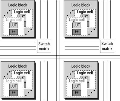
Figure 2.10 A high-level block diagram of a simple FPGA consisting of logic blocks, logic cells, storage elements, function generators, and routing logic.
2.3.6 Special-Purpose Function Blocks
So far we have focused on internals of the FPGA’s configurable (or programmable) logic. A large portion of the FPGA consists of logic blocks and routing logic to connect the programmable logic. However, as semiconductor technology advanced and more transistors became available, FPGA vendors recognized that they could embed more than just configurable logic to each device.
Platform FPGAs combine programmable logic with additional resources that are embedded into the fabric of the FPGA. A good question to ask at this point is “why embed specific resources into the FPGA fabric?” To answer this we must consider FPGA designs compared to ASIC designs. An equivalent ASIC design is commonly considered to use fewer resources and consume less power than an FPGA implementation. However, ASIC designs are not only often found to be prohibitively expensive, the resources are fixed at fabrication. Therefore, FPGA vendors have found a compromise with including some ASIC components among the configurable logic. The exact ASIC components are vendor specific, but we will briefly cover in this section a few of the more commonly seen components. The components range in complexity from embedded memory and multipliers to embedded processors. The following paragraphs introduce some of these components with more detail to be found in Section 2.A and throughout the rest of the book.
The block diagram of a Platform FPGA, seen in Figure 2.11, shows the arrangement of these special-purpose function blocks placed throughout the FPGA. Which function blocks are included and their specific placement are determined by the physical device; this illustration is meant to help the reader understand a general construct of modern FPGAs. The logic blocks still occupy a majority of the FPGA fabric in order to support a variety of complex digital designs; however, the move to support special-purpose blocks provides the designer with an ASIC implementation of the block as well as removes the need to create a custom design for the block. For example, a processor block could occupy a significant portion of the FPGA if implemented in the logic resources.
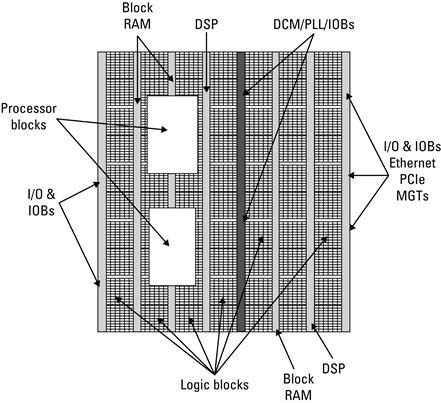
Figure 2.11 A high-level view of a Platform FPGA.
Block RAM
Many designs require the use of some amount of on-chip memory. Using logic cells it is possible to build variable-sized memory elements; however, as the amount of memory needed increases, these resources are quickly consumed. The solution is to provide a fixed amount of on-chip memory embedded into the FPGA fabric called Block RAM (BRAM). The amount of memory depends on the device; for example, the Xilinx Virtex 5 XC5VFX130T (on the ML-510 developer board) contains 298 36 Kb BRAMs, for a total storage capacity of 10,728 Kb. Local on-chip storage such as RAMs and ROMs or buffers can be constructed from BRAMs. BRAMs can be combined together to form larger (both in terms of data width and depth) BRAMs. BRAMs are also dual-ported, allowing for independent reads and writes from each port, including independent clocks. This is especially useful as a simple clock-crossing device, allowing one component to produce (write) data at a different frequency as another component consuming (reading) data.
Digital Signal Processing Blocks
To allow more complex designs, which may consist of either digital signal processing or just some assortment of multiplication, addition, and subtraction, Digital Signal Processing Blocks (DSP) have been added to many FPGA devices. As with the Block RAM, it is possible to implement these components within the configurable logic, yet it is more efficient in terms of performance, and power consumption to embed multiple of these components within the FPGA fabric. At a high level, the DSP blocks of a multiplier, accumulator, adder, and bitwise logical operations (such as AND, OR, NOT, and NAND). It is possible to combine DSP blocks to perform larger operations, such as single and double precision floating point addition, subtraction, multiplication, division, and square root. The number of DSP blocks is device dependent; however, they are typically located near the BRAMs, which is useful when implementing processing requiring input and/or output buffers.
Processors
Arguably one of the more significant additions to the FPGA fabric is a processor embedded within the FPGA fabric. For many designs requiring a processor, often choosing an FPGA device with an embedded processor (such as the FX series part for the Xilinx Virtex 5) can simplify the design process greatly while reducing resource usage and power consumption. The IBM PowerPC 405 and 440 processors are examples of two processors included in the Xilinx Virtex 4 and 5 FX FPGAs, respectively. These are conventional RISC processors that implement the PowerPC instruction set. Both the PowerPC 405 and the 440 come with some embedded system extensions but do not implement floating-point function units in hardware. Each come with level 1 instruction and data cache and a memory management unit (MMU) with a translation look-aside buffer to support virtual memory. A variety of interfaces exist to connect the processors to the FPGA programmable logic to allow interaction with custom hardware cores.
Not all FPGAs come with a processor embedded into the FPGA fabric. For these devices the processor must be implemented within the FPGA fabric as a soft processor core. This text is not affected adversely by the decision to include or remove processors from within the FPGA fabric. Instead this book is aimed at providing the reader with the necessary skill set to use the available resources as efficiently as possible to solve the given problem. It would be unwise to ignore a discussion of hard processor cores merely on speculation.
Digital Clock Manager
Most systems have a single external clock that produces a fixed clock frequency. However, there are a number of reasons a designer might want to have different logic cores operating at different frequencies. A Digital Clock Manager (DCM) allows for different clock periods to be generated from a single reference clock. You could use logic to divide an existing clock signal down to generate a lower frequency clock — say 100 to 25 MHz. While possible, the correct design practice is to use a DCM to generate the slower clock. The advantage of using a DCM is that the generated clocks will have lower jitter and a specified phase relationship. Section 2.A gives more specific details on how to use DCMs in a Xilinx design.
Multi-Gigabit Transceivers
Over the last 20 years, digital I/O standards have varied between serial and parallel interfaces. Serial interfaces time-multiplex the bits of a data word over fewer conductors while parallel interfaces signal all the bits simultaneously. While the parallel approach has the apparent advantage of being faster (data are being transmitted in parallel), this is not always the case in the presence of noise. Many recent interfaces — including various switched Ethernet standards, Universal Serial Bus (USB Implementers Forum (USB-IF) 2010a, b, SerialATA (Grimsrud, Knut and Smith, Hubbert 2003), FireWire (1394 Trade Association 2010), and InfiniBand (Futral 2001) — are now using low-voltage differential pairs of conductors. These standards use serial transmission and change the way data are signaled to make the communication less sensitive to electromagnetic noise.
High-Speed Serial Transceivers are devices that serialize and deserialize parallel data over a serial channel. On the serial side, they are capable of baud rates from 100 Mb/s to 11.0 Gb/s, which means that they can be configured to support a number of different standards, including Fiber Channel, 10G Fiber Channel, Gigabit Ethernet, and Infiniband. As with the other aforementioned FPGA blocks, the transceivers can be configured to work together. For example, two transceivers can be used to effectively double the bandwidth. This is called channel bonding (multilane and trunking are common synonyms).
This initial overview does not encompass all of the available resources on every FPGA device. It does provide a comprehensive overview of the significant components often used in FPGA designs. More details are forthcoming for these components and their applicability and implementation within embedded systems designs. For the interested reader, a more detailed explanation of how to construct these basic FPGA elements from CMOS transistors is presented in Chow et al. (1991) and Compton & Hauck (2002).
2.4 Hardware Description Languages
Now that we know what is inside of an FPGA, the next step is to learn how to “configure” them. We use a hardware description language (HDL) as a high-level language to describe the circuit to be implemented on the FPGA. Most courses in digital logic nowadays introduce HDLs in the context of designing digital circuits. Unfortunately, some very popular HDLs were never intended to be used as they are today. The origins of hardware description languages were rooted in the need to document the behavior of hardware. Over time, it was recognized that the descriptions could be used to simulate hardware circuits on a general-purpose processor. This process of translating an HDL source into a form suitable for a general-purpose processor to mimic the hardware described is called simulation. Simulation has proven to be an extremely useful tool for developing hardware and verifying the functionality before physically manufacturing the hardware. It was only later that people began to synthesize hardware, automatically generating the logic configuration for the specified device from the hardware description language.
Unfortunately, while simulation provided a rich set of constructs to help the designer test and analyze the design, many of these constructs extend beyond what is physically implementable within hardware (on the FPGA) or synthesize inefficiently into the FPGA resources. As a result, only a subset of hardware description languages can be used to synthesize designs to hardware. The objective of this section is to present two of the more popular hardware description languages, VHDL and Verilog. It is arguable to which is better suited for FPGA design; both are presented here for completeness, but it is left to the readers to decide which (if any) is best suited for their needs. We will focus on VHDL throughout the remainder of this book as it becomes redundant to give two examples, one in VHDL and one in Verilog, for every concept. That being said, we will also focus within this section on synthesizable HDL and how it maps to the previous section’s components.
2.4.1 VHDL
VHDL, which stands for VHSIC1 Hardware Description Language, describes digital circuits. In simulation, VHDL source files are analyzed and a description of the behavior is expressed in the form of a netlist. A netlist is a computer representation of a collection of logic units and how they are to be connected. The logic units are typically AND/OR/NOT gates or some set of primitives that makes sense for the target (4-LUTs, for example). The behavior of the circuit is exercised by providing a sequence of inputs. The inputs, called test vectors, can be created manually or by writing a program/script that generates them. The component that is generating test vectors and driving the device under test is typically called a test bench.
Synthesizable VHDL
In VHDL, there are two major styles or forms of writing hardware descriptions. Both styles are valid VHDL codes; however, they model hardware differently. This impacts synthesis, simulation, and, in some cases, designer productivity. These forms are:
Structural/data flow circuits are described in terms of logic units (either AND/OR/NOT gates or larger functional units such as multipliers) and signals. Data flow is a type of structural description that has syntactic support to make it easier to express Boolean logic.
Behavioral circuits are described in an imperative (procedural) language to describe how the outputs are related to the inputs as a process.
A third style exists as a mix between both structural and behavioral styles. For programmers familiar with sequential processors, the behavioral form of VHDL seems natural. In this style, the process being described is evaluated by “executing the program” in the process block. For this reason, often complex hardware can be expressed succinctly and quickly — increasing productivity. It also has the benefit that simulations of certain hardware designs are much faster because the process block can be executed directly. However, as the design becomes more complex, it is possible to write behavioral descriptions that cannot be synthesized. Converting behavioral designs into netlists of logic units is called High-Level Synthesis, referring to the fact that behavioral VHDL is more abstract (or higher) than structural style.
In contrast, because the structural/data-flow style describes logic units with known implementations, these VHDL codes almost always synthesize. Also, assembling large systems (such as Platform FPGAs) requires structural style at the top level as it is combining large function units (processors, peripherals, etc.). Also, it is worth noting that some structural codes do not synthesize well. An example of this is using a large RAM in a hardware design. A RAM is not difficult to describe structurally because of its simple, repetitive design. However, in simulation, this tends to produce a large data structure, which needs to be traversed every time a signal changes. In contrast, a behavioral model of RAM simulates quickly because it matches the processor’s architecture well.
VHDL Syntax
All components of a design expressed in VHDL consist of an entity declaration followed by one or more declared architectures. The entity declaration describes the component’s interface — its inputs, outputs, and name. By analogy, it is a function prototype in C or a class header file in C++.
The architecture block, in contrast, provides an implementation of the interface. VHDL allows for more than one implementation. Why? One reason is the simulation/synthesis issue just mentioned. One architecture might be used for simulation and another for synthesis. A second reason is different architectures might be needed for different targets (ASIC versus FPGA).
Starting with an empty source file, the program usually begins by including some standard library definitions. VHDL uses Ada’s syntax for this by first stating a library’s name and then which modules from that library to use via the library and use keywords. Next comes the entity declaration followed by one or more architecture blocks. The simplest way to learn this syntax is to study some examples. Consider the 3-input, 2-output full adder circuit in Listing 2.1.
The entity block says that the name of this component is fadder and that it has five ports. A port can be an input (in), output (out), or both (inout) to the component. In this example there are three inputs and two outputs. The signals can be of any primitive type defined by the VHDL language or a complex type. In our example, we use a complex type that was defined by the library “ieee” called std_logic. We use this to model a single Boolean variable with the binary value of either ‘0’ or‘1’.
The architecture block defines how the entity is to be implemented. It has a name as well (imp_df) and, in this example, only uses the data-flow style to describe how the outputs are related to its inputs. The following are some initial notes regarding VHDL. First, VHDL is not sensitive to case. The strings cin and CIN are the same variable; begin and bEgIn are both legal ways of writing the begin keyword. Second, the input and output ports can be
described on the same line like a, b have been defined or they can be placed on separate lines like cin. Inputs and outputs cannot be specified on the same line. Also, ports of different types (even if they are the same direction) cannot be specified on the same line. Third, the name of the architecture (imp_df) is user specific and does not have to follow any specific convention. Each subsequent architecture for the same entity must have unique architecture names. Finally, signal assignment is denoted by the <= operator. This is often a cause for syntax errors for those more familiar with C/C++ or Java syntax.
So how does the full adder map to hardware? With two outputs both depending on three inputs, two function generators are needed. Depending on the FPGA device, this may be reduced to a single LUT (if using 6-LUTs) or two LUTs. No D flip-flops are needed as there is no clock source, so the circuit represents a purely combinational circuit.
Now that we have built one component, we can use it to design a slightly more sophisticated component. In Listing 2.2 a 2-bit full adder is implemented. In this design, additional logic has been added for academic purposes; this may not be the ideal implementation of such a component. We are using it to highlight a number of VHDL-specific constructs.
In this example we have added clock and reset inputs and changed a, b and sum from std_logic to std_logic_vector(1 downto 0), a 2-bit signal. Next, we add internal signals to register the inputs and outputs. This is not a requirement, but it is recommended to buffer these signals to meet tighter timing constraints as signals are passed from a top-level component down to the low-level 1-bit full adder components. This is followed by the fadder component declaration, which indicates which components will be used within this design. Within the beh architecture, a VHDL process named register_proc is added. This process is used to register the inputs and outputs on the rising edge of the clock signal. This code infers all of the D flip-flops within the logic cells. The reset signal rst is a synchronous reset, which is recommended over asynchronous resets. This simplifies the reset logic needed to route the asynchronous signal across the chip. Finally, two 1-bit full adder component instances are included. Note that the internal signal carry_tmp connects the carry-out from bit 0’s full adder to the carry-in of bit 1’s full adder.
The resulting 2-bit full adder circuit consumes more resources than the single bit full adder. By adding registers to the input and outputs, we have extended the full adder’s resource count by eight D flip-flops. Two flip-flops are needed for each input a, b and output sum and one flip-flop is needed for the input cin and output cout. Also, a third LUT is included for the carry-in/out logic.
The previous example was used to show the use of a VHDL process statement to infer D flip-flops and how to instantiate other VHDL components. It is not the intention of this book to teach the reader all of the details of VHDL, as there are far better books available for this purpose. Instead we are “priming the pump,” giving the reader some VHDL now to help get the process started. Throughout the rest of the book, additional examples will be provided that are suited for specific embedded systems designs or recommendations on how to write VHDL to correctly infer the desired components that lead to more efficient designs. We conclude this VHDL subsection with one final example, a finite state machine (FSM). A finite state machine can be used for a variety of purposes, such as sequence generators and detectors, and is well suited for embedded systems design.
In this example we use an FSM to perform 8-bit addition. This is similar to what was done earlier except that we will add the constraint that the two operands are not guaranteed to be aligned. That is, the operands may or may not arrive at the same time and we must keep track of when both have arrived before adding the results together. This may be due to single access to data memory or data arriving from two different sources. Either way, the FSM will wait for one of the operands to arrive, register it, and then wait for the second operand to arrive, register it, and then add them together. The primary goal of this example is to explain how to use finite state machines in VHDL; there may be more effective ways to implement this example, but we will leave those more elegant solutions to the reader.
The FSM example in Listing 2.3 contains several new features beyond the first two examples. The most significant is how to use VHDL to describe a finite state machine. There are different
ways to go about describing the FSM, but we have chosen what is considered a two-process finite state machine. There are also one-process and three-process FSMs, but the two-process FSM is arguably the most common. For those familiar with the traditional two-process finite state machine, this particular implementation may seem a little different. We present a variation on the popular two-process FSM because we find it more efficient and effective for the programmer. Specifically, we eliminate the redundant description of states in separate processes as it is a common place for design errors. Before we get too far ahead of ourselves, let’s take a step back for those less familiar with finite state machines in VHDL.
To begin, a special VHDL signal type must be declared to differentiate the states in the finite state machine. This is done by adding the line:
type FSM_TYPE is (wait_a_b, wait_a, wait_b, add_a_b);
This line creates a new type (similar to a typedef or enumerate in C), which contains four states: (wait_a_b, wait_a, wait_b). Then, two signals are added of the type FSM_ TYPE and initialized to the first state wait_a_b called fsm_cs and fsm_ns for the finite state machine’s current state and next state indicators.
In addition to the state signals, we include additional registers for intermediate inputs. As was done with the second example (2-bit adder), we will register specific signals to help alleviate potential timing constraints, yielding higher operating frequencies (clock rates) for the component. These two signals are a_reg and b_reg, which have accompanying signals a_next and b_next. These signals behave just like the current/next state registers and will be used to hold the operands a and b inputs when they are valid, denoted by a_we and b_we being asserted.
To help illustrate how the fsm_cs and fsm_ns signals are used, consider Figure 2.12. A sequential circuit is built from both combinational logic and state registers. This is covered in an introductory digital logic course; we expand on it a little to include registering internal signals (a_reg, b_reg). Each clock cycle the state register is updated based on the combination logic next state output. In VHDL, this is done with one, two, or three processes. We are using a two-process FSM to help differentiate the state register and combinational logic. In the fsm_register_proc process, the state signal is registered.
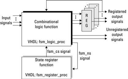
Figure 2.12 The VHDL process with the corresponding sequential digital circuit for finite state machines.
In the fsm_logic_proc process, the combinational logic is described, including state transitions and each state’s output. Here, a VHDL case statement is used for the finite state machine. The initial state is wait_a_b. The state transition is based on if the input a and/or b arrive. There are three possible conditions: both a and b arrive in unison, a arrives before b, or b arrives before a. If a and b arrive at the same clock cycle the inputs are registered and the FSM transitions to the add_a_b state. If a arrives before b, then a is registered and the FSM transitions to the wait_b state. Likewise, if b arrives before a, b is registered and the FSM transitions to the wait_a state. If neither a or b arrives, then the FSM stays in this initial state.
In both the wait_a and the wait_b states, we already know that one of the two operands has already arrived and is registered so we are just waiting for the opposite input. Once it arrives, we register it and transition to the add_a_b state, where the two operands are added and the output is set. The valid signal is used to notify whatever component is dependent on the result output that is now ready.
There are some important notes to address with this example. First is the sensitivity list ; that is, the list of signals that a process waits on for changes that cause the process to be re-evaluated. In simulation, if a signal (say a_we) is omitted, then even if that signal changes, it will not necessarily cause the process to be re-evaluated. This can cause the system to behave differently from what is expected or desired. In hardware the process is always running; hardware does not get invoked like a C function call. As a result, the sensitivity list will be automatically generated by the synthesis tools. Care must be taken by the designer when simulating the design, and sensitivity list omissions are often an example of a design error that will cause simulation and synthesis results to not match. We say all of this because while we find simulation extremely useful as both a design and a debug tool, the designer must use simulation tools intelligently with the mindset of writing synthesizable VHDL.
Clearly this was only intended to be an introduction to VHDL for the reader. The examples chosen were picked to give the reader a sampling of code to begin to play with when designing new components. Often the hardest part of any language is getting past the first hump of practical examples. For further VHDL reading we recommend Ashenden, Peter J. (2008). If you instead are interested in seeing what else is commonly used, we present Verilog next.
2.4.2 Verilog
Another common hardware description language is Verilog. Verilog has many similarities to VHDL, as both were originally intended to describe hardware circuit designs. Verilog is considered to be less verbose than VHDL, often making it easier to use, especially for designers more familiar with an imperative coding style such as C++ or Java. As with VHDL, Verilog became more than just a textual representation of a circuit. Designers used Verilog to simulate circuits that eventually led to a subset of the language supporting hardware synthesis. This section is written to provide the reader with a sufficient set of examples to begin to learn Verilog. The examples are based on those presented in the VHDL section, but with Verilog syntax. As was noted previously, this book focuses primarily on VHDL, but the reader should take care to familiarize themselves with both VHDL and Verilog, as they are both used within industry and academia. As with VHDL, there is a significant amount of resources already available for Verilog and should the reader find Verilog to be the more comfortable HDL, we encourage the reader to use Verilog. While this book may be more VHDL centric in its examples, the underlying ideas and concepts are applicable to both HDLs.
Synthesizable Verilog
In Verilog, there are three major styles or forms of writing hardware descriptions. Both styles are valid VHDL codes; however, they model hardware differently. This impacts synthesis, simulation, and, in some cases, designer productivity. These forms are:
Verilog Syntax
All components of a design expressed in Verilog consist of modules. Starting with an empty source file, the program usually begins with the keyword module followed by the module’s name and ports. The ports are then defined in terms of input and output along with individual types, such as single bits or bit vectors. Unlike VHDL, there are no explicit libraries to include at the beginning of each file. For demonstration purposes, consider the same 1-bit full adder example presented in the VHDL section written in Verilog, shown in Listing 2.4.
The module is named fadder, which has five ports. A port can be an input, output, or both (inout) to the module. In this example, there are three inputs and two outputs. The data type can be a wire, register, integer, or constant. We will give specific examples shortly. Each of the inputs and outputs in this example is a single bit representing binary ’1’ or ’0’. One important note regarding syntax is that Verilog is case sensitive and all keywords are lowercase; that is, wire is a Verilog data type, whereas Wire is a unique variable name.
Unlike VHDL, there is no formal distinction between the module interface and the design’s logic. In the full adder example, the keyword assign is used with combination circuit assignment. The line
assign sum = a ^ b ^ cin
infers a three input xor gate with the output connected to the sum output. The symbols &, ![]() represent bitwise and, or, xor, not, respectively.
represent bitwise and, or, xor, not, respectively.
So how does the Verilog full adder map to hardware? Not surprisingly, it maps to the same resources as VHDL implementation. With such a simple example it is easy for the synthesis tool to infer the same logic, correctly.
Extending the Verilog 1-bit full adder to a 2-bit full adder as was done with VHDL will provide additional Verilog constructs and the conciseness of Verilog becomes more apparent. Listing 2.5 shows the 2-bit full adder example. The reg keyword is used for register declarations, and the wire keyword is used for internal combinational interconnects. The equivalent of a VHDL process block is the always block. In this example, inputs and outputs are registered to the input clock’s rising edge, inferring D flip-flops. Two instances of the 1-bit fadder component follow, connecting the inputs, outputs, and carry logic accordingly. The components
for bit 1 and bit 0 are named fa1 and fa0, respectively. Finally, the module’s outputs (sum and cout) are assigned the registered output values. The resulting circuit utilizes the same number of resources as the VHDL version.
Finally, we present the finite state machine example in Verilog in Listing 2.6. Here is where the biggest difference between
Verilog and VHDL can lie. It is possible to code FSMs similar to the VHDL implementation or completely different. We have chosen to closely match the two implementations, but we recommend those with an interest in Verilog to purchase one of the many Verilog HDL books available to learn the other possible implementations.
The most noticeable difference is the syntax; in fact, with this implementation you could set both files side by side and see an almost one-to-one mapping between the two languages. We chose to continue to use a two-process (always block) finite state machine and a case statement for its implementation. One difference is rather than using a type to define the FSM as was done in VHDL, we use a parameter and encode each state.
The reader may notice that the Verilog section is shorter than VHDL. This is not by chance. The authors favor VHDL, we make no attempt to hide this fact. We do not fault Verilog; in actuality we find Verilog a delightful language and offer the fact that we learned VHDL first (and Ada) as our only definite reason for our tendency toward VHDL. This section tried to provide some examples of Verilog that a reader can use with additional material to further pursue Verilog as a hardware description language. For those interested in a additional Verilog reading, we recommend Ashenden, Peter J. (2007).
Regardless of the language choice, we strongly suggest the reader take note of what is considered synthesizable HDL. When creating components, take the time to synthesize each component individually and understand how the component is being mapped to hardware. This will give you a better understanding of the resources needed by both the component and the final design.
2.4.3 Other High-Level HDLs
While the majority of hardware engineers use either VHDL or Verilog, there are other HDLs available. Because we are focusing on VHDL, we will not go into specific details about these additional languages at this time. In an effort to increase productivity, SystemC Open SystemC Initiative (OSCI) (2010), HandelC Agility (2010), and Impulse Impulse Accelerated Technologies (2010) are a few of the attempts at building hardware and software systems together by providing the designer a higher level language to work in. Some are extensions to the C/C++ library, while others use C-like syntax to provide a more programmer-friendly environment. Some do provide designers with an alternative to the verification of a complete hardware/software system, which can be carried out before further hardware/software partitioning. Moreover, when translating existing algorithms into hardware-implementable architecture, preserving the source programs in C or C++ becomes possible with the support of an intelligent compiler, which may only involve a minor effort of code modification. Overall, it is debatable whether these languages are mature enough to support the desired goal of providing the design with the ability to model large systems, which incorporate both hardware components and software applications.
2.5 From HDL to Configuration Bitstream
So far in this chapter we have covered the internals of the FPGA, along with hardware description languages that provide a mechanism to describe complex digital circuit designs. As mentioned earlier, the process of converting an HDL into logic gates is called synthesis and the result of this process is a netlist file. This section describes how to convert a digital circuit to a netlist. Then, it describes how to configure an FPGA device from the netlist. A more detailed example of this process with vendor-specific tools is provided in Section 2.A.
Let’s start with an example. Consider the Boolean function:
![]()
The schematic is shown in Figure 2.13. This circuit is easily expressed in a netlist. Each of the gates (two OR gates and one AND gate) becomes a “cell.” Each primitive cell will include the type of gate, a name for this cell, and a set of ports. Ports will have names and direction (input or output). Complex cells can be formed by adding contents, which are instances of other cells and nets. Nets describe how the cells are “wired up”; that is, which output ports are connected to which input ports. Since complex cells can include other complex cells, a netlist forms a hierarchy with a single top-level cell encompassing all other cells. Ports on the top-level cells are then associated with external pins on the FPGA device.
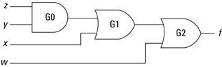
Figure 2.13 Schematic of a simple Boolean function.
There are many netlist formats and most are binary (i.e., not human readable) but some, such as EDIF, use a simple syntax and ASCII text to describe a cell hierarchy. EDIF (pronounced E-diff ) stands for Electronic Design Interchange Format and is a vendor-neutral standard. Different tools use different file extensions. Some use .edif but others have adopted various three-letter suffixes to be compatible with DOS file name restrictions such as .edf and .edn. To give the reader a flavor for its format, a stripped down sample is shown in Figure 2.14. One last comment, the primitive cells used in a netlist are not universal. They may be basic logic gates (AND, OR, etc.) or they can be vendor-specific components (like a TBUF) that a vendor’s back-end tool flow knows about.
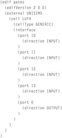
Figure 2.14 Portions of a Boolean function in EDIF.
The process we want to explain is how to go from a computer-readable expression of a digital circuit to a sequence of bits suitable to configure an FPGA. Using the example described earlier, ![]() , the first thing to recognize is that we have four inputs — so
, the first thing to recognize is that we have four inputs — so ![]() cannot be implemented in a single 3-LUT function generator. With only three select lines, an 8-to-1 MUX can only handle three variables. The solution is to use two 3-LUTs and and the routing resources to connect them. For example,
cannot be implemented in a single 3-LUT function generator. With only three select lines, an 8-to-1 MUX can only handle three variables. The solution is to use two 3-LUTs and and the routing resources to connect them. For example, ![]() can be decomposed into two functions:
can be decomposed into two functions: ![]() , where
, where ![]() and
and ![]() . Now
. Now ![]() and
and ![]() can be used to configure two 3-LUTs. The output of
can be used to configure two 3-LUTs. The output of ![]() is routed to the second input of
is routed to the second input of ![]() . This decomposition is illustrated graphically in Figure 2.15.
. This decomposition is illustrated graphically in Figure 2.15.
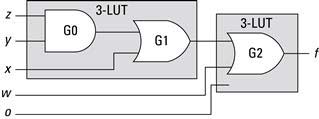
Figure 2.15 Example of a four-input function mapped to two 3-LUTs.
Note that G1 could be part of either 3-LUT — the result is the same (two function generators are required). Also note that if a 3-LUT only has two inputs, then the third select line is connected to ground and half of the SRAM entries are don’t cares.
The process of grouping gates and assigning functionality to FPGA primitives is called mapping or MAP for short. The result of mapping a netlist is another netlist. The difference is that the cells of the input are generic Boolean gates; the cells of the output are FPGA primitives (3-LUTs, Flip-Flops, TBUFs, etc.).
The next step in the back-end tool flow is to assign the FPGA primitives in the netlist to specific blocks on a particular FPGA device. This process is called placement. In our simple example, ![]() uses two 3-LUTs. During placement, the tools will decide which two 3-LUTs to use and add that information to the netlist.
uses two 3-LUTs. During placement, the tools will decide which two 3-LUTs to use and add that information to the netlist.
Because every 3-LUT is the same as every other 3-LUT, the real challenge here is to place the cells relative to one another such that routing the output of one 3-LUT to the next one has the lowest propagation delay. Recall from Section 2.3 an output from the logic block goes to a connect box. From the connect box, a pass transistor decides where the signal propagates, which may be an adjacent logic block or to a switch box. A pass transistor is able to either propagate or block a signal by connecting the gate of the transistor to an SRAM cell, allowing the transistor to control the signals in a general-purpose circuit. If the signal goes to a switch box, another pass transistor determines which wire segment to use and so on to the next switch box and eventually to a connect box and a logic block. Every transistor and, to some extent, the length of the wire segments used contribute to the propagation delay. The longest propagation delay in the design will determine the maximum clock frequency. The process of picking wire segments and setting passing transistors is called routing.
If the project requires something like a 100-MHz clock frequency, but the design has a propagation delay that limits the clock to say 50 MHz, we say that the design does not meet timing. For very large netlists that use a large fraction of the resources, it is possible (and fairly common) that bad placement will use all of the routing resources in one area of the chip, making it impossible to connect all of the nets in the netlist. When this happens, we say the design failed to route.
In either case — not meeting timing or failing routing — the solution is to try a different placement to see if that produces less congestion or shorter routes. In fact, because placement and routing are so tightly coupled, they are considered a single step and one place-and-route tool (PAR). Early place-and-route algorithms did things like (1) randomly place all of the cells and then (2) route each signal sequentially. If a signal cannot be routed, throw away all the routes and start with a different signal. If it appears routing is going to always fail, throw out everything and randomly place all of the cells again. The process continues until all of the signals are routed or some threshold for giving up is met! Today, the tools are more sophisticated but the specific algorithms are trade secrets that vendors keep to themselves. The drawing in Figure 2.16 illustrates the concepts of our running example after PAR. The SRAM cells are organized in a 2-D array (additional logic not shown).
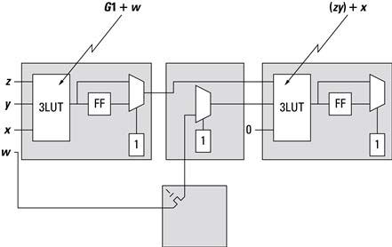
Figure 2.16 Illustration of ![]() placed and routed.
placed and routed.
The final step is to convert this 2-D collection of SRAM cell settings into a linear stream of bits. One can imagine all of the cells arrayed into two dimensions. One column might be associated with a column of 3-LUTs on the chip. All of the SRAM cells that make up each 3-LUT would be stacked on top of each other. The next column might have all of the SRAM cells used to configure the connect and switch boxes. The next would be another column of 3-LUTs. All of these SRAM cells are connected vertically as shown in Figure 2.17 to form a giant shift register. To set the SRAM cells, the first column of data is shifted into place, followed by the next column and so on. So the last step, called bitgen, takes a placed and routed netlist and sets the SRAM cells of this large 2-D array accordingly. Along with a header, each of the columns is written out sequentially to a binary file called a bitstream.
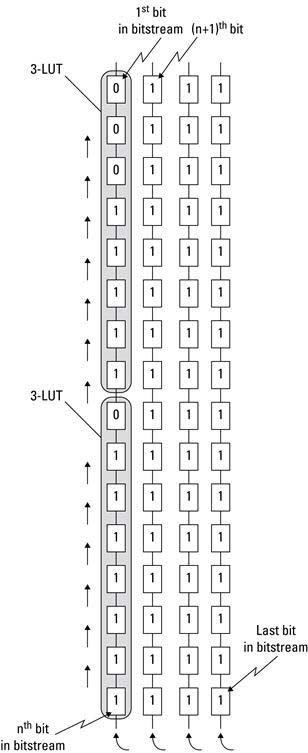
Figure 2.17 Illustration of ![]() placed and routed.
placed and routed.
Again, this is not exactly how any vendor configures an FPGA but this illustrates enough details that a system designer needs to know.
Chapter in Review
This chapter covered a wide range of material, some of which may be considered background reading or act as a refresher for the reader. Our intention in this chapter was to emphasize material that we believe the reader should be aware of and, if not, provide enough detail to quickly catch the reader up to speed for the rest of the book.
At the heart of the FPGA is the CMOS transistor. We are keenly interested in this technology not because we are physically specifying and implementing transistors in our designs, but because all of the reconfigurable technology rests on top of it. Therefore, being aware of its characteristics, such as power consumption, will benefit the embedded systems designer. In addition to transistors, a brief overview of programmable logic devices was given with the intention to explain how FPGAs evolved into what they are today and to possibly provide some insight into the direction FPGAs may go in the future.
The cornerstone of this chapter was the discussion on FPGAs and Platform FPGAs. In Chapter 1 we covered some details about FPGAs, but here we dwelled into the specific constructs of the device. Just as a painter must be familiar with the available colors, so should the designer be familiar with the low-level components of the device.
This led into hardware description languages where we discussed how to describe hardware in both VHDL and Verilog. This was again meant to be a quick review or introduction to the language, as the purpose of this book is not to teach the reader everything about HDLs. Finally, we covered how to generate a bitstream from the HDL so we can configure the FPGA and run our hardware design on the actual device.
Practical Expansion
The Target
This chapter’s white pages covered a wide range of material that is essential for designing systems with FPGAs. Throughout the gray pages we provide more technical details with respect to Xilinx FPGAs, Xilinx tool chain, and VHDL. For some readers, the white pages are sufficient to illustrate the point; however, we feel that practical examples with existing FPGA devices are more often what solidifies the readers, understanding of the material.
Toward this end we use a single device from a family of FPGAs, the Xilinx Virtex 5 (XC5VFX130T-FF1768). The goal is to learn the details of this device, build up a vocabulary of terms, explore several low-level ways of configuring an FPGA, and cover the design process from concept to implementation to running system. From there, it is relatively easy to learn a different device by comparing their features and functionality.
There are two more advantages to learning how to configure the low-level internal details of an FPGA. First, when the need arises, it is possible for an engineer to forgo the high-level tools and build a device-specific, efficient hardware module. (By analogy, most embedded systems are programmed in high-level languages but there are rare occasions that call for subroutine to be written in assembly.) The second reason — and this is very important with state-of-the-art high-level tools — is that oftentimes an engineer needs to understand how a small change in a high-level language may affect the eventual implementation in an FPGA. That is, with today’s tools it is easy to break a working design by making a simple change to a high-level construct that ends up requiring twice as many FPGA resources.
These gray pages begin with a more detailed view of the Xilinx Virtex 5 FX130 FPGA. This material is available from the Xilinx Web site; however, aggregating the material is useful for someone new to the area or unfamiliar with how all of the technical documents and details are related. Next, a more detailed overview of the Xilinx Integrated Software Environment (ISE) tool chain is presented to help clarify each step in the FPGA configuration process. Finally, through the use of a few Xilinx tools, a custom hardware core and components will be developed and downloaded to the board.
2.A Xilinx Virtex 5
To start, the Xilinx Virtex 5 FPGA series consists of several related but different devices. The groups are denoted LX, SX, TX, and FX. What do they all mean? In short, they refer to different mixes of configurable logic blocks and hard cores on the device. The LX (and any variants such as LXT) refers to devices that have a large number of configurable logic blocks relative to other hard cores on the device. The resources on the FPGA are more heavily allocated to configurable logic than say a processor embedded into the FPGA fabric. The SX refers to signal processing series parts, allocating more resources toward digital signal processing applications. The TX/HX refers to parts that have additional high-speed serial transceivers for high bandwidth interconnection capacity. The FX refers to FPGAs that have one or more PowerPC’s embedded into the FPGA fabric.
It is possible to build Platform FPGAs from devices that do not include a hard processor. In that case, one or more soft processor cores can be used within the configurable logic. We focus on the FX series parts with two PowerPC 440 hard processor cores. The reason for this is because a majority of our embedded systems designs rely on at least a single processor, using a hard processor is a better use of FPGA resources as it consumes less power, has a higher operating frequency, and requires less physical space than an equivalent FPGA implementation.
2.A.1 Look-Up Table
Xilinx refers to the function generators within the FPGA fabric as look-up tables (LUT). The Virtex 5 FPGAs are built from 6-input LUTs. The white pages refer to 3-input LUTs for demonstration purposes (an 8-row truth table/Boolean circuit is much easier to represent than a 64-row truth table in a book); however, today’s devices include larger 4-LUTs and 6-LUTs.
In practice, using hardware description languages (HDL) to describe the digital circuit and then using synthesis tools to map the textual description, an equivalent look-up function is more common than the designer defining the LUTs logic itself. What is important as far as the designer is concerned is how to represent a circuit efficiently to utilize the available resources. The 6-LUT on the Virtex 5 can be used either as a single 6-LUT or as two 5-LUTs as long as both 5-LUTs share the same inputs. A designer can take advantage of this when building digital circuits by not including the unnecessary inputs, which the synthesis tools may infer to a larger LUT. Figure 2.18 represents the block diagram of a 6-LUT. In the event that all six inputs are used for the LUT, the bottom output O5 is not used.
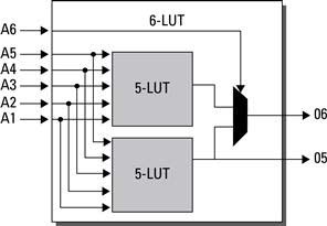
Figure 2.18 The Virtex 5 6-input LUT actually is built from two 5-input LUTs with the sixth input controlling a mux between the two LUTs.
2.A.2 Slice
In the white pages we presented the term logic cell to represent a look-up table and a storage element (D flip-flop). The Virtex 5 combines four of these logic cells to create a slice, as is shown in a simple block diagram in Figure 2.19. With four 6-LUTs and D flip-flops contained within close proximity, it is possible to use these components to design more complex circuits. In addition to Boolean logic, a slice can be used for arithmetic and RAMs/ROMs. Some slices are connected in such a way that they can be used for data storage as distributed RAMs or shift registers. This is accomplished by combining multiple LUTs in the slice. The distributed RAM can be configured as single, dual, and, in some cases, quad ports providing independent read-and-write access to the RAM. The depth of the RAMs varies based on the number of ports, but can range from 32 to 256 1-bit elements. The distributed RAMs’ data width can be increased beyond 1-bit; however, there will be a trade-off between the width and depth and the resource usage. For example, a 64 × 8 (64 8-bit elements) RAM is implemented in nine LUTs (1-LUT per 64 × 1 RAM and an additional LUT for logic). However, a 64 × 32 extends beyond an efficient use of the configurable resources and is moved into what will be discussed shortly, Block RAM (BRAM).
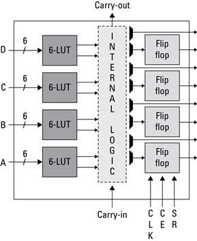
Figure 2.19 A block diagram of a Virtex 5 logic slice with four 6-LUTs and four flip-flop/latch storage elements.
In addition to logic and memory, slices can be used as shift registers. A shift register is capable of delaying an input x number of clock cycles. Using a single LUT, data can be delayed up to 32 clock cycles. Cascading all four LUTs in one slice, the delay can increase to 128 clock cycles. This is useful for small buffers that would traditionally be implemented within a more valuable resource, such as a Block RAM.
In all of these possible uses, a D flip-flop can be added to provide a synchronous read operation. With the additional D flip-flop, a read will be subject to an additional latency of one clock cycle. This may or may not impact a design, but for designs with high timing constraints, adding the synchronous operation can relax the constraint.
2.A.3 Configurable Logic Block
In the Virtex 5, a configurable logic block (CLB) contains two slices and the carry logic to connect neighbor slices. A CLB is considered the highest level of abstraction for the FPGA’s configurable fabric. The two slices within the CLB are not directly connected, instead they sit in what is considered separate slice columns. Each CLB is connected to a switch matrix, providing configurable designs to span many CLBs. The switch matrix consists of long and short wires to provide more direct, point-to-point connections between CLBs in close proximity. Figure 2.20 depicts the basic structure and interconnection of CLBs, slices, and switch matrices.

Figure 2.20 Virtex 5 CLB block diagram of the interconnection between each slice in the CLBs and their connection to the switch matrix.
2.A.4 Block RAM
Block RAM is dedicated random access memory grouped together in 36 Kbit blocks on Virtex 5 FGPAs. This is in addition to the distributed RAM mentioned earlier. BRAM provides on-chip memory, which can be used as large look-up tables, local storage, or data buffers (FIFOs). Each BRAM has two independent access ports (A and B) that only share data in the memory cells. Clocks are relative to each port. Care must be taken when using BRAMs in dual-port mode where the two ports write to the same address at the same time instance. This will not cause any ill effects to the physical BRAM, but effectively a race condition occurs between the two ports and it is nondeterministic which port’s data will be actually stored in the memory cells. It is not difficult to design around this problem, but being aware of the problem before writing any designs makes the problem all the easier.
BRAMs are configurable in the width and depth supported. Each 36-Kb BRAM can be configured as 32K × 1 (32,768 by 1 data bit), 16K × 2, 8K × 4, 4K × 9, 2K × 18, or 1K × 36 RAMs. The depth and width are related to produce a maximum of 36-Kb. A BRAM can be combined with an adjacent BRAM to provide deeper or wider BRAMs.
Likewise, a BRAM can be split as two independent 18-Kb RAMs. Each 18-Kb RAM can be configured as a 16K × 1, 8K × 2, 4K × 4, 2K × 9, or 1K × 18. This provides the Virtex 5 FPGAs with an ability to utilize their resources more efficiently.
One common use of BRAMs in FPGA designs is for FIFOs. FIFOs, or simply data queues, are primitives designers can take advantage of, rather than building their own out of BRAM logic, reducing design and debugging time. Recently, FPGAs have started to include FIFOs as separate components within the FPGA fabric. The Virtex 5 and 6 are two such devices, although the physical limitations on the functionality may rule out their use in a design. We cover FIFO primitives in more detail in Section 6.A. For now, we focus on the use of BRAMs for storage and large buffers within Platform FPGA designs.
2.A.5 DSP Slices
A common use for FPGAs is with digital signal processing (DSP). The need to perform operations in parallel and to customize the operations based on the application has increased in the community of FPGA-based DSP designers. To improve the performance, many FPGAs come with special DSP blocks. In the Virtex 5, the DSP slices are known as DSP48E (48-bit DSP element) slices.
The DSP slices include a 25 × 18 two’s complement multiplier, 48-bit accumulator (for multiply accumulate operations), an adder/subtractor for pipelined operations, and bitwise logical operations. Embedding this functionality into the slice provides a significant savings in FPGA resources, as implementing the equivalent resources in LUTs is quite expensive.
For applications needing filters, such as a comb and finite impulse response, to transforms, such as fast and discrete Fourier, to CORDIC (coordinate rotational digital computer) algorithm, DSP slices are used when available. The Virtex 5 FX130T on the ML-510 contains 320 DSP slices. Compared to 20,480 regular slices, this seems like a disproportionate amount, yet not all designs require the use of DSP slices.
For designs requiring a higher percentage of DSP slices, the Xilinx SX series FPGAs include more DSP resources. There are tools, one of which we will introduce shortly, that help the designer quickly implement customized DSP components. They are also useful for resource and performance approximation.
2.A.6 Select I/O
Interfacing off the FPGA is another important issue when designing for embedded systems. In most cases, there will be a need to interface with some physical device(s). Depending on the number of I/O pins required, some devices are better suited than others, but they are all built around Input/Output Blocks.
From Figure 2.21 each I/O tile spans two pads (which connect to physical pins). Each Pad connects to a single IOB, which connects to the input and output logic. Xilinx uses the term Select I/O to refer to configurable inputs and outputs, which support a variety of standard interfaces (LVCMOS, SSTL, LVDS, etc.). Select I/O also take advantage of Digitally Controlled Impedance (DCI) to eliminate adding resistors close to the device pins, which are needed to avoid signal degradation. DCI can adjust the input or output impedance to match the driving or receiving trace impedance. Some advantages include a reduction in the number of parts, which simplifies the PCB routing effort. It also provides a way to correct for variations in manufacturing, temperatures, and voltages.
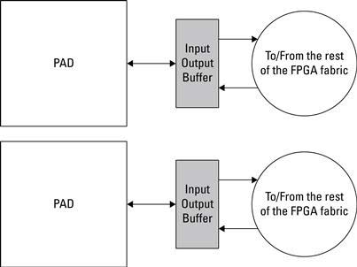
Figure 2.21 Xilinx Select Input/Output buffer (IOB) tile for connections between FPGA fabric and the pad on the FPGA device.
2.A.7 High-Speed Serial Transceivers
Along with Select I/O, some FPGAs include additional high-speed transceivers (transmit/rec-eive) to connect devices serially at low latency and high bandwidth. The transceivers are coupled within the FPGA fabric to provide direct access to and from soft cores. Line rates are programmable from 100 Mb/s to 6.5 Gb/s. In the Virtex 5 series FPGAs, two types of transceivers exist, RocketIO GTX and GTP. GTX transceivers are capable of a higher bandwidth, whereas GTP transceivers are lower bandwidth and require less power. The number of transceivers varies from part to part. For example, the Virtex 5 FX130T includes 20 GTX transceivers. As with DSP slices and SX series FPGAs, there are applications that require a higher percentage of transceivers to configurable logic. The TX (also known as TXT or HX) series FPGAs include these additional transceivers. Both GTX and GTP transceivers are bidirectional, providing independent transmit and receive at the same time.
The transceivers can support parallel data through use of the serialize/deseralize (SERDES) logic, which connects to the input/output blocks. To support higher bandwidth needs, it is possible to bond the channels together. For example, two transceivers operating at 5.0 Gb/s bonded together can offer 10.0 Gb/s bandwidth at the cost of the additional transceiver resource. In high bandwidth-sensitive applications, the extra resource is a necessary expense.
Xilinx includes a customizable GTX/GTP wizard to expedite adding the transceiver logic to a design or specific component. In short, it is possible to specify the data width (parallel data), frequency, and channel bonding needed by the design. Design considerations are needed for systems with tight timing or resource constraints; however, much of the headache typically associated with high-speed integration can be eliminated.
2.A.8 Clocks
In FPGA designs it is common to operate different cores at different frequencies. In traditional design, any clocks needed would have to be generated off-chip and connected as input to the system. With FPGA designs it is possible to generate a wide range of clock rates from a single (or a few) clock source(s). While it is easier to design systems with only a few different clock rates, having the flexibility to incorporate clock rates after board fabrication is compelling to designers. However, there are limitations on the number of clocks that can be generated and routed to various parts of the FPGA. A number of clock regions exist on the FPGA (varying from 8 to 24 based on the Virtex 5 FPGAs), which support up to 10 clocks domains. The FPGA is split in half and on each half a clock region spans 20 CLB. The Virtex 5 FX130T has 20 clock regions. Figure 2.22 is a simple example of the clock regions on the FPGA.
Figure 2.22 Clock regions on an FPGA span 20 CLBs vertically and half of the FPGA horizontally; the number of clock regions varies by chip.
To help design, use, and manage these clocks, Xilinx uses digital clock managers (DCM). Generally speaking, a DCM takes an input clock and can generate a customizable output clock. By specifying the multiply and divider values, the frequency-synthesis output clock clkfx can generate a custom clock. Given an input clock clkin the equation:
![]()
is used to generate the output clock. However, the DCM provides more than just generating different clock rates. A DCM is also capable of phase shifting the input clock by 90, 128, and 270 degrees. The DCM also provides a 2× the input clock rate and can phase shift this input clock by 180 degrees. It is easy to see without going into more detail that DCMs are a useful tool to generate the necessary clock(s) in FPGA designs. In short, meeting timing when designing with FPGAs can be a difficult task unless design considerations for timing and clocks are included from the beginning of the design process.
2.A.9 PowerPC 440
The Virtex 5 FX series FPGAs include one or two PowerPC 440 (Xilinx, Inc., 2009b) processors embedded within the FPGA fabric. The PowerPC 440 is a RISC processor with an operating frequency of up to 550 MHz. It contains a seven-stage pipeline with out-of-order execution capabilities. Included are data and instruction 32 KB, 64-way set associative level 1 caches.
The PowerPC connects to a system bus known as the Processor Local Bus (PLB), which is part of IBM’s CoreConnectIBM (2009) suite of soft cores. The PLB supports 128-bit data transfers at user-define frequencies (in most cases, 200 MHz is the upper limit, but more discussion on the PLB will come in Section 3.A). A example of the processor’s block diagram is shown in Figure 2.23.
Figure 2.23 PowerPC 440 processor block diagram showing the available interfaces between processor and FPGA fabric.
In addition to the PLB, the PowerPC 440 includes a crossbar switch. The switch is used to connect the processor to a memory controller for a high bandwidth, low latency connection to off-chip memory. The switch also supports up to four direct memory access (DMA) ports, enabling more efficient transfers to and from memory to soft compute cores implemented within the FPGA fabric. We go into more detail regarding DMA in Chapter 4.
Another unique feature of the PowerPC is the auxiliary processing unit (APU). The APU connects to the fabric coprocessor bus (FCB) to support custom instructions implemented in the FPGA fabric. For example, a double precision floating point unit (FPU) can be connected to the APU. Then, anytime the application needs to perform a floating point computation, the processor will offload the computation to hardware where the computation can be performed faster than a software-emulated FPU.
The PowerPC will be at the heart of our initial Platform FPGA designs. The PowerPC provides us with a “comfortable” environment (for those more familiar with C/C++ than HDLs) to begin to interact with the various components and, soon, our own custom soft cores.
Overall, we mention these components not because a designer is forced to implement Boolean logic or distributed RAMs at such a low level; ideally that is what the hardware description languages and synthesis tools are for. Instead, we mention them to help clarify for the reader the flexibility available with FPGA designs and to illustrate a point. The designer should not place too much dependency on low-level tools to create resource-efficient and high-performing designs. For example, being able to identify when a design is better suited for BRAM FIFOs instead of LUTs and specifying that information within the HDL context make the synthesis tool’s job easier. Finally, we mention these different components to help a designer understand what their design is being mapped to. It is a gratifying feeling when a designer can look at a synthesis report and understand where and why all of the resources are being used and, if necessary, modify their design to take better advantage of the remaining resources.
2.B Xilinx Integrated Software Environment
2.B.1 Overview of Commands
The Integrated Software Environment (ISE) contains a suite of commands that can turn FPGA designs described in hardware description languages and netlists into bitstream configuration files. ISE is a comprehensive program and there are plenty of tutorials and FAQs available. Instead, we aim to cover the underlying commands (Xilinx, Inc. 2009a) that are called by the ISE GUI. For those more comfortable with the ISE GUI, it is hoped that this section will at least clarify what each step is in the hardware synthesis process.
Xilinx Synthesis Tool
At the core of the ISE tool chain is the Xilinx Synthesis Tool (Xilinx, Inc. 2009c)(XST). XST is used to synthesize hardware description languages into a netlist. XST is not the only synthesis tool available; however, as it is available within the ISE tool chain, it will be the synthesis tool used throughout this book.
To help in our understanding of how XST works, we begin by synthesizing the VHDL version of the 1-bit full adder. In addition to the VHDL file, two files are needed to run XST in command line mode. These two files are the project file and the synthesis script file. The project file specifies all of the HDL in the project to be synthesized. It is commonly named with the extension .prj. In the full adder example, only one VHDL file exists so the project file simply contains:
vhdl work fadder.vhd
The three columns denote the HDL type, library name, and VHDL filename. The work library is the default library to use.
The XST synthesis script is commonly named with the extension .scr. This script contains parameters used by XST during synthesis. It is possible to run XST without a script by entering each option on the command line; however, creating a single script is the preferred method, as it reduces redundant typing of the long series of inputs at the command line. For the full adder example, the synthesis script is shown in Figure 2.24.
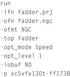
Figure 2.24 Example of a synthesis script for XST.
The run keyword will indicate to XST to execute synthesis with the following attributes. XST requires an input project filename (ifn), which is the project file we mentioned earlier, containing the HDL to be synthesized. The output filename (ofn) is the name the synthesized netlist will be given after successful synthesis. The output file format (ofmt) is set to NGC, Xilinx’s proprietary netlist format.
Next is the top-level entity name (top) attribute, which in our full adder example is fadder. Two synthesis optimization options follow, one that specifies whether XST should synthesize for speed (provide the highest operational frequency possible) or area (pack the logic as tightly as possible). The second option is for the synthesis effort level. A trade-off between synthesis effort and synthesis time is made; higher levels may provide more resource efficient or frequency efficient designs at the expense of longer synthesis times. The iobuf attribute adds I/O Buffers to the top-level module. In the full adder example, we choose not to insert I/O Buffers. The last attribute in this example is the FPGA part type (p). Here we specify to synthesize for the Virtex 5 FX 130T FPGA.
Additional command line arguments can be added to the synthesis script file; however, for this first XST example these are sufficient to produce a netlist. The final step is to run XST on the command line, passing the synthesis script file as an input file.
xst -ifn fadder.scr
After XST completes, a report is written to a synthesis report file (srp). If there are any syntax errors, XST will report approximately where in the file the line exists that failed synthesis. This is similar to compiling a C binary. Understanding the report is an important tool for the designer when trying to identify resource consumption and timing analysis. Under the Final Report heading, in Figure 2.26 is a list of the basic elements (BELS) needed to represent the digital circuit. In our design, two 3-LUTs are needed for the two outputs, sum and carry-out, in the full adder.
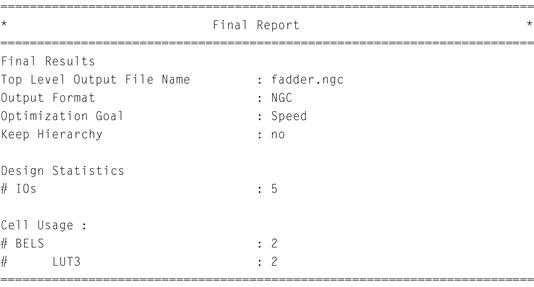
Figure 2.25 XST synthesis final report section.
Figure 2.26 XST synthesis report device summary section.
Another important section in the synthesis report file is the device utilization summary section, in Figure 2.27. For the specific FPGA device the number of slices, LUTs, flip-flops, BRAMs, and so on are listed, giving the designer an approximation to the amount of resources the design requires.
Figure 2.27 XST synthesis timing report.
The synthesis report also provides some rough timing information, in Figure 2.28. These numbers are not accurate because they do not consider the actual placement of the circuit on the FPGA. It does provide an approximation to the minimum period and maximum combination delay the circuit can obtain. Looking at the report, our full adder example was purely combinational, there is no clock and as a result no minimum period. For larger designs when trying to meet timing, the synthesis report can help identify which component is causing the timing error.
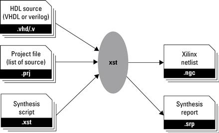
Figure 2.28 Synthesis flow.
For large systems with many components and subcomponents, XST can be used to synthesize the entire design into a single netlist or it can be used to synthesize individual components in a hierarchical fashion. Figure 2.25 depicts this synthesis flow for a design. While each approach has their merits, the second approach is used more often as it provides more immediate and useful feedback for each component. This approach stems from the philosophy of bottom-up design where components are created (typically in HDL) from the ground up. It is only natural to synthesize in the same fashion, generating intermediate netlists and producing individual synthesis reports. The designer can view these reports to determine which of the components need to be redesigned in the event of resource or timing constraints.
For example, consider a design consisting of three components, a top-level component and two low-level components. XST would be used to synthesize the top-level and two low-level components individually. The top-level component synthesis would treat the two low-level components as black boxes. The immediate advantage of such an approach is to minimize the number of times each component needs to be resynthesized. If one of the low-level components of HDL is modified, only that low-level component requires being synthesized again, unless the modification changes the entity’s generic or port list, forcing the top-level component to change its instantiation of the design. These are akin to how libraries are in C/C++ during compile time.
Netlist Builder
After XST is used to generate the system’s netlist(s), the next step is to combine the netlists and any specific design constraints to produce a single netlist file. This is typically accomplished through the use of the following two commands, NGCBuild and NGDBuild.
NGCBuild
If the designer has chosen to synthesize each component individually in a hierarchical manner, the next command needed is called ngcbuild, which combines multiple netlist files into a single ngc netlist. NGCBuild opens the top-level netlist and matches any subcomponents with existing netlists. NGCBuild does not produce errors or warning when one or more subcomponent’s netlists are not found. In the previous example, the top-level component netlist may be combined with one of its two subcomponents in the event that only one of the two components has been synthesized. NGCBuild can be called again to combine the missing subcomponent netlist when it is available. This is similar to the component level synthesis approach mentioned earlier in that a component’s netlist is constructed as its subcomponents become available. An example of the NGCBuild command line execution is:
% ngcbuild input/system.ngc output/system.ngc -sd implementation
The input to NGCBuild is the top-level netlist (in this example it is input.ngc). The output netlist generated by NGCBuild is the second parameter (output.ngc). The flag -sd specifies the search directory to look for any component’s netlist to be combined to generate the output netlist.
NGDBuild
Once all of the components have been synthesized, ngdbuild is used to generate a Xilinx Native Generic Database (NGD) file. The NGD file is used to map the logic contained within the netlist to the specific FPGA device. NGDBuild takes a single NGC file (created by NGCBuild) and any device, netlist or user constraints file. User constraints would include specific FPGA pins to be used for components such as RS232 UARTs and off-chip memory like DDR2 modules. NGDBuild will produce errors during run time if any of the netlists are missing in the input NGC file or if there are unbound user constraints. An example of NGDBuild is:
% ngdbuild -p xc5vfx130tff1738-2 -bm system.bmm -uc system.ucf system.ngc system.ngd
The command line flags used by NGDBuild are -p to specify which FPGA device to generate the ngd file for, -bm to specify the block memory file, which is a listing of all of the BRAMs in the system, and -uc to specify the constraints file listing all of the design’s constraints (timing, IO, IO Standards). The final input is the NGC file generated by NGCBuild. The single output is the NGD file that will be passed on to Map, the next stage in the tool flow.
Map
The Xilinx program MAP takes an NGD file and maps the logic to the specified FPGA device. MAP performs a design rule check (DRC) to uncover physical or (if possible) logical errors in the design. After passing the DRC, the logic described by the netlist is mapped to the FPGA device’s components (such as BRAM, IOBs, and LUTs). MAP also trims any unused logic or netlists. Unlike synthesis, which can only trim internal signals if they are not used, MAP analyzes the entire system to determine if any logic is unnecessary. As a result, after MAP completes, the resource utilization reported is a more accurate representation than the synthesis report. We previously used the synthesis report’s resource utilization to give us an approximate first-order estimation of the resources needed by the design; now we can rely upon MAP’s report. When finished, MAP produces a Native Circuit Description (NCD) file, which can be used by the next tool to place and route the design to the target FPGA. An example of MAP’s command line is:
% map -o system_map.ncd -pr b -ol high system.ngd system.pcf
The MAP flags are used to give the designer more control over what MAP placements are or are not run. Typically, a designer will be able to use the default options; however, there are cases when a nearly fully occupied FPGA design may require additional constants to MAP successfully. The -o flag sets the output file name; in this case the resulting NCD file is named system_map.ncd. The -pr b option specifies to pack flip-flops and latches in both input and output registers, while the -ol high flag is the overall effort level for the placement algorithm; high is used to achieve the best placement at the expense of longer MAP run times. The input file, system.ngd, is the NGD file generated by NGDBuild. We already stated that system_map.ncd is the output from MAP, but in addition it is system.pcf, the physical constraints file, which are constraints placed during the design creation.
Place and Route
The Xilinx program PAR actually consists of two programs, Place and Route. These two programs are commonly run in series, so Xilinx has combined them into a single command. PAR takes the NCD file generated by MAP and runs both placement and routing algorithms to generate a routed NCD file. To begin, Place tries to assign components into sites (LUTs, BRAMs, DSP48E slices, etc.) based on any specific constraints (i.e., use pin location P38 to output the transmit (TX) line of the RS232 UART component) to maximize resource utilization while minimizing component distances (which will make routing and meeting timing requirements easier). Placement occurs through multiple phases (passes) and produces a placed NCD file.
After Place, Route is run to connect all of the signals for the components based on the timing constraints. Routing is also a multiphase operation, resulting in a routed NCD file. After PAR completes, a timing analysis is performed to verify that the design has met timing and, if not, produce a short log to help the designer identify and fix the errors. As the design size and clock rates increase, timing becomes more constrained and difficult to meet. It is possible to run PAR with different command line arguments in order to meet timing. PAR consumes the most time during the execution of all of the tools (as the design increases). Identifying fast build computers to run PAR on will reduce the amount of “idle” time before a design can be tested on the FPGA. An example of an PAR command line is:
% par -ol high system_map.ncd system.ncd system.pcf
PAR takes as input the NCD file and PCF files from MAP and generates an output system.ncd file, which is the placed and routed native circuit description.
Figure 2.29 illustrates the flow from netlists to a fully placed and routed design. This flow picks up after the Figure 2.25 that is run for each component in the design. These flows are used to help picture the process from source files (HDL) to just before generation of a bitstream, which is covered next.
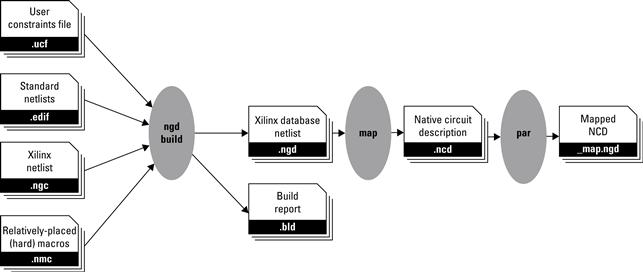
Figure 2.29 Netlist builder, map, and place-and-route.
Configuration Bitstream Generation
The final command in generating a configuration file for the FPGA is called bitgen. BitGen produces a configuration bitstream for the specific Xilinx FPGA device. The bitstream (.bit) file contains configuration information (proprietary to Xilinx), which is downloaded and stored into the SRAM cells of the FPGA device. The concept of programming an FPGA is when the bitstream is downloaded to the FPGA, at which point the digital circuit is realized on the FPGA fabric. An example of the BitGen command line is:
% bitgen -f bitgen.ut system.ncd system.bit
The BitGen command can take as input a parameters file (-f bitgen.ut), which can be used to specify configuration information. The output system.bit is the configuration bitstream that can be used to “program” the FPGA.
Additional commands can be used during the synthesis and bitstream generation process; however, their uses are more application specific. We will hold off on covering those designs until later chapters where their use is better understood.
These short sections have covered the process from synthesis to bitstream in an effort to better understand the entire ISE flow and, when the need arises, to fix problems and to know where to look to identify the problems. Initially, it is easiest to use the XPS GUI to create complex designs and then use the GUI to synthesize, map, place and route, and generate the bitstream. However, as you gain more experience you may become more interested in the low-level commands that are producing the various log and report files. Going forward we encourage you to at least look at the logs and reports generated by these commands and then, if you are comfortable, try to execute these commands on your own.
2.C Creating and Generating Custom IP
Up until now we have been laying a foundation of terms and technology, and with the addition of hardware description languages we have begun to learn how to build upon this foundation. We have also covered the commands used by Xilinx’s ISE, which provides us with the tools to turn the HDL into a bitstream used to program the FPGA.
In addition to ISE, there are tools that can aid in the rapid development of components and cores. In this section two of these tools will be presented along with a detailed example of how to use them to generate custom components and cores.
2.C.1 Xilinx Core Generator
Xilinx Core Generator (CoreGen) is a tool that designers can use to quickly create hardware components. These components can range in complexity from FIFOs and math operators to DSP filters and transforms to network and memory controllers. While CoreGen unfortunately does not generate every type of component, it does provide a sufficient number to help most designers get their projects started. Earlier we mentioned FIFOs as being one of the more useful components, here we show how to use CoreGen to quickly generate a customized FIFO.
To start, from the command line run the command coregen and create a new project, specifying which FPGA device will be used when generating the FIFO. This is necessary because of the different FPGA devices and packages, and their supporting FPGA resources. If you are using the Xilinx ML-510 development board, then you can specify the Virtex 5 xc5vfx130t-ff1738 part. Figure 2.30 shows the main CoreGen GUI with the FIFO Generator component selected, ready to be run for the next step. The left half of the GUI is a list of the IP that can be generated with CoreGen. The upper right half lists information and actions relevant to the selected IP component, while the lower right half is a console to show output information, warnings, and errors. Now we are able to pick from a list of available components. Under the Memories & Storage Elements category are CAMs, FIFOs, Memory Interface Generators, and RAMs and ROMS. For this example we will select FIFOs and double click on FIFO Generator.
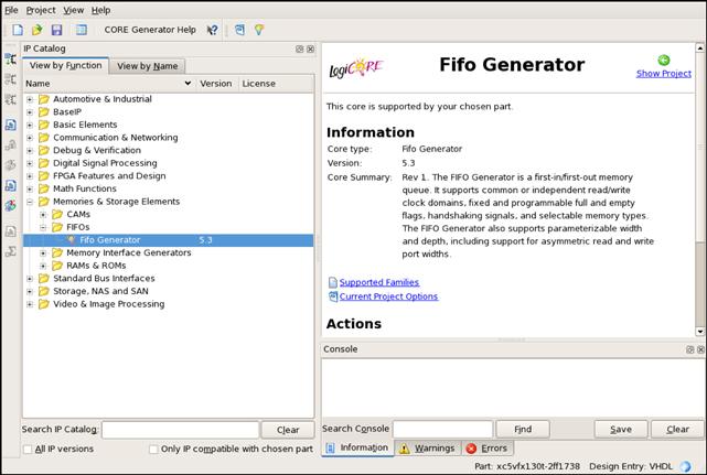
Figure 2.30 Main Xilinx CoreGen GUI.
The first page of the FIFO Generator wizard, Figure 2.31, lets you specify the component name and FIFO implementation type. We have named our component fifo_comp and set it to be a Common Clock Block RAM implementation. From our previous discussions on RAM we can start to see how CoreGen gives us the ability to specify constraints (such as common vs independent clocks) and we are able to see what type of memory options are supported.
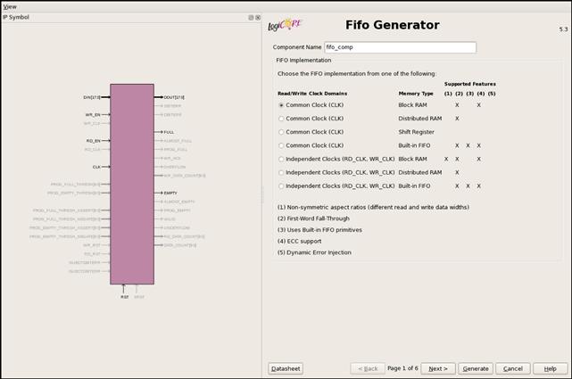
Figure 2.31 CoreGen’s FIFO Generator initial configuration page.
In the second page (Figure 2.32) we can specify the read mode, port width, and depth of the FIFO. In a standard FIFO read mode, when data are read from the FIFO via the read request (dequeue) signal, read data will be valid the next clock cycle. The first-word fall-through FIFO eliminates the single cycle read latency by storing the head of the FIFO in a register. Each subsequent read request pops the next element off the FIFO and stores it in the head register. These design decisions are less important in this example, but for latency sensitive designs it can play an important role in the system. For now, select the standard FIFO read mode.
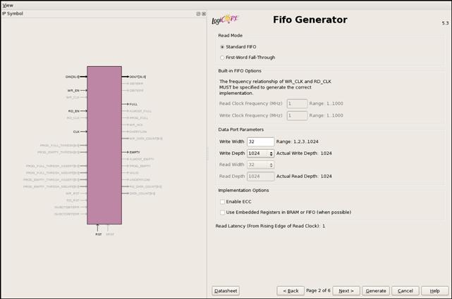
Figure 2.32 CoreGen’s FIFO Generator read mode and FIFO options page.
At this point we can also specify the depth and width of the FIFO. Because we have selected a common clock BRAM, the width and depth are fixed for both the write and the read sides of the FIFO. If we had selected an independent clock implementation we could specify independent port parameters. For this example we use a write width of 32 bits and a depth of 1024 data elements. Recall that the 1K × 32 configuration requires a single 36-Kb BRAM. CoreGen gives us the ability to increase the depth without requiring us to write the HDL to cascade the BRAMs.
Figure 2.33 shows the third page, which provides the design with the ability to specify additional flags and handshaking ports. Depending on the amount of control needed in the design, these ports may or may not need to be added. The valid flag is a signal that will be assert high (’1’) when valid data are on the dout port of the FIFO.
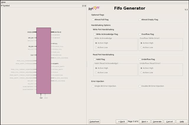
Figure 2.33 CoreGen’s FIFO Generator handshaking signals page.
In the fourth page the initialization/reset options are set, as can be seen in Figure 2.34. Here it is possible to have either a synchronous reset or an asynchronous reset and what the default output should be after a reset. An important note, when a FIFO is reset, both empty and full flags will be asserted high, indicating data should not be read from or written into the FIFO. Once the reset is complete, the full signal will be deasserted, indicating the FIFO is ready for operation.
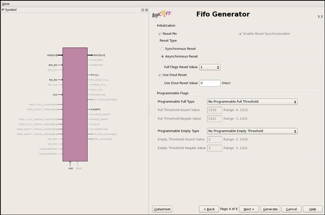
Figure 2.34 CoreGen’s FIFO Generator initialization and programmability page.
There is also an ability to add programmable full and empty flags. For data-flow purposes it might be important to have high and low watermarks for the FIFOs. When the FIFO reaches a predetermined threshold, the programmable full signal would be asserted high. Likewise a programmable empty signal can be used in the event a FIFO nears becoming empty. These programmable thresholds provide user-defined values for the FIFO compared to the almost_full and almost_empty signals, which are only asserted one data element before the respective signal is asserted.
Figure 2.35 shows page five of the FIFO generator, which provides the designer with the option to output a count of the number of data elements in the FIFO at any given time. This may be useful under conditions when a design needs to perform different operations based on the status of the FIFO.
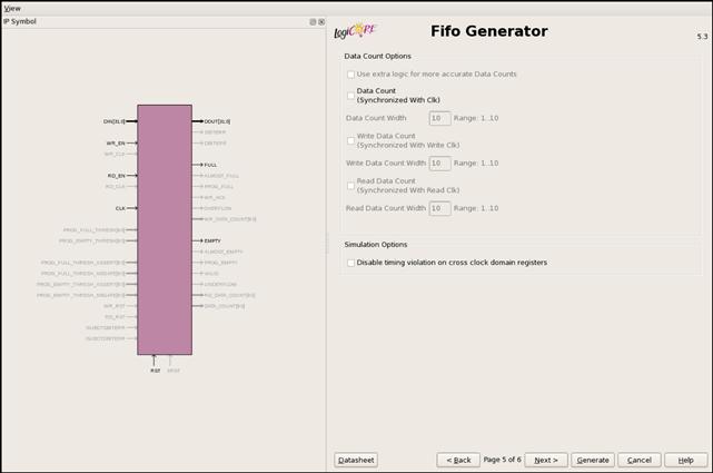
Figure 2.35 CoreGen’s FIFO Generator data count page.
The final page, Figure 2.36, provides a summary of the options taken by the designer and, most importantly, relays the resources based on those configuration settings. In our example, we have a 1K × 32-bit FIFO, which results in a single 36K BRAM being used.
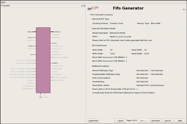
Figure 2.36 CoreGen’s FIFO Generator summary page.
At this point all that is left is to generate the FIFO. Once complete, a set of files are produced that provide simulation HDL (.vhd), HDL component declaration and instantiation templates to be used within calling HDL (.vho), and the proprietary Xilinx netlist file (.ngc), which will be used by the synthesis tools when the FIFO component is instantiated by the top-level component. A README is also provided, which details the remaining files generated automatically by CoreGen.
2.C.2 Create/Import Peripheral Wizard
In Section 1.A the Xilinx Platform Studio was introduced. With XPS we are given a rich set of GUI applications and wizards to expedite the base system building design process. We have already been introduced to the base system builder wizard. Using the Create/Import Peripheral (CIP) wizard we will generate a hardware core template. This template will give us the ability to read and write into software addressable registers. In Section 1.A we augmented this hardware core to support more functionality. In the meantime, we focus on the CIP wizard.
We can launch the CIP wizard from within the XPS GUI menu option:
![]()
or by launching the wizard from the command line:
% createip
Once the wizard launches, you will walk through the following pages.
Figure 2.37 Create/import peripheral wizard welcome page.
The first page of the wizard is a simple welcome screen, which explains that the core you will be creating will be for an EDK CoreConnect-based project. In our case, this means we will be creating a core that will connect to the Processor Local Bus.
The second page is the peripheral flow; here we have the ability to create a new core (based on a template) or import and modify an existing peripheral. For now, we will continue with creating a template for a new peripheral.
The next page indicates where this project will be added, to an existing repository or directly into a project. Because this is the first core that we have created, this can be added to the existing project that was created previously at the beginning of this section. (Note: the path may differ based on where you saved your project.)
The fourth page lets us set the core’s name and version number. There are characters that are not allowed in the name, the core contain any uppercase characters, start with a number or symbol, or end with a symbol. When naming the core, if the text turns red it indicates an invalid core name. We will name our coremy_test_core.
On the next page we specify which bus our core will be able to attach. The PLB allows the PowerPC to communicate with our core. This will be the most common interface for PowerPC-based systems.
Figure 2.38 Create/import peripheral wizard peripheral flow page.
Figure 2.39 Create/import peripheral wizard project page.
Figure 2.40 Create/import peripheral wizard name and version page.
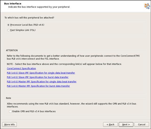
Figure 2.41 Create/import peripheral wizard bus interface page.
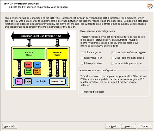
Figure 2.42 Create/import peripheral wizard IPIF page.
On the sixth page we can specify what interface our core will have to the PLB. This is known as the IPIF (Intellectual Property Interface). The PLB IPIF simplifies the number of signals and the complexity of the handshaking required to connect a custom core to the PLB. Here we will only add User logic software registers, allowing the processor to read and write to registers that will be created in our my_test_core. The registers provide a simple interface to exchange data and control signals between the processor and our core.
The slave interface page provides the core with the ability to support burst and cache-line transfers and nonnative data widths (beyond 32 bit). The PLB can support up to 128-bit transfers; however, the PowerPC is a 32-bit processor so for this first example we will continue with the default 32 bits.
The next page lets us set the number of software-addressable registers within the core. When the wizard generates the core’s template, these registers and all of the necessary read-and-write logic will be included. We begin with three registers to help us demonstrate how to read and write to our core from the PowerPC.
The ninth page is the IP Interconnect (IPIC). These are the signals that our my_test_core’s user logic HDL will interact with. The IPIF mentioned earlier is responsible for interfacing with the PLB and generating the appropriate IPIC signals. The IPIC signals are a much simpler set of bus interface signals, abstracting the complex bus signals away from the designer. For now we will stick with the default IPIC signals. Signals beginning with Bus2IP are input ports to the core from the PLB, and signals beginning with IP2Bus are output ports from the core to the PLB.
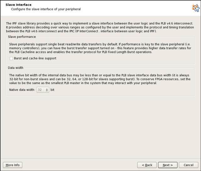
Figure 2.43 Create/import peripheral wizard slave interface page.
The next page provides an optional simulation support through use of a bus functional model (BFM). The BFM provides a cycle accurate simulator of the PLB, aiding in the design process by providing a quick simulation test bench for the custom core as if it were connected to the PLB. At this time we will skip the BFM; however, it will become very advantageous to use simulation when designing as it provides a quicker and easier debugging method than debugging a custom core running in hardware.
The next page explains the HDL structure of the created core. There will be two HDL files created, a top-level component (in our case named my_test_core.vhd) and the User Logic (user_logic.vhd). The user logic will contain the initial HDL to provide the PowerPC access to the core. At this page we can also specify the user logic’s hardware description language as Verilog instead of the default, which is VHDL.
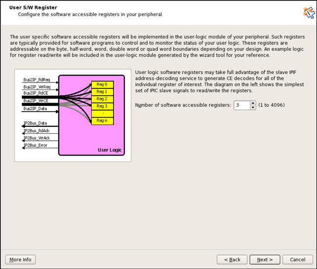
Figure 2.44 Create/import peripheral wizard slave registers page.
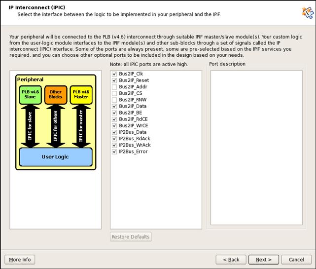
Figure 2.45 Create/import peripheral wizard IPIC page.
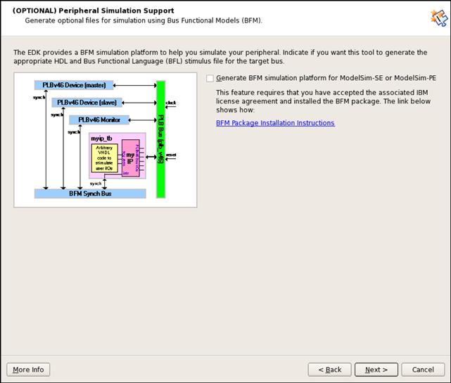
Figure 2.46 Create/import peripheral wizard simulation page.
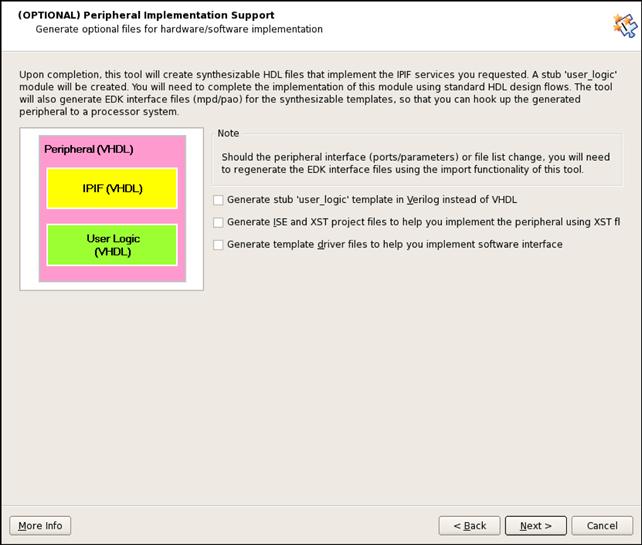
Figure 2.47 Create/import peripheral wizard support page.
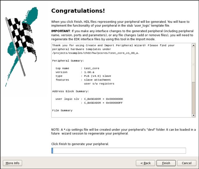
Figure 2.48 Create/import peripheral wizard summary page.
Finally, the last page is the summary of the core that will be created. Once the IP core is generated we can look to see how the core’s project directory is organized.
2.C.3 Hardware Core Project Directory
The create and import peripheral wizard generates a new hardware core’s project directory inside the pcores directory. In our example we named the pcore my_test_core_v1_00_a. Within this directory are the subdirectories and files shown in Figure 2.49.
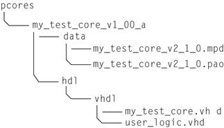
Figure 2.49 Xilinx hardware core’s pcore directory structure.
Within the data directory are two files, my_test_core_v2_1_0.mpd, which is the Microprocessor Peripheral Description (MPD), and my_test_core_v2_1_0.pao, which is the Peripheral Analysis Order (PAO). These files are mentioned because in order to augment the hardware core, we will need to modify these files.
Microprocessor Peripheral Description File
The MPD file contains project options, bus interfaces, generics, and ports for VHDl (or Verilog). Peripheral Options are used by the Xilinx EDK during Platform Generation (PlatGen), the stage before synthesis, to set up the synthesis script for XST. Bus Interfaces are a list of bus standards available in the EDK, such as the PLBV46 (Processor Local Bus v4.6). The bus interface is used to aggregate all of the bus signals (address, data, etc.) together to make connectivity of components to buses in the EDK easier. For example:
BUS_INTERFACE BUS = SPLB, BUS_STD = PLBV46, BUS_TYPE = SLAVE
Generics/Parameters are equivalent to the generics and parameters in a VHDL entity or Verilog module. These are the generics located in the top-level VHDL file in our hardware core, my_test_core.vhd. Assigning a default value in the MPD file for a generic will overwrite the default value given in the VHDL file. By placing a generic in the MPD file, it exposes the generic to the MHS file to be modified by the designer in the EDK. The parameters are specified with a name, default value, data type, and additional parameters depending on the data type. For example,C_SPLB_DWIDTH:
PARAMETER C_SPLB_DWIDTH = 128, DT = INTEGER, BUS = SPLB, RANGE = (32, 64, 128)
The priority of setting a component’s generics is as follows:
1. set in the MHS File (highest priority)
Ports, like generics, are used to connect the top-level entity to the rest of the system. In order to add an additional port in the top-level entity in a hardware core, it must also be added to the MPD file so that it will be visible to the EDK. The ports are specified with the port name, a default value (or connection to a bus interface), a direction, a vector size (if necessary), and a bus connection (if necessary). For example, PLB_wrDBus is the write data bus for the hardware core that is connected to the PLB.
PORT PLB_wrDBus = PLB_wrDBus, DIR = I, VEC = [0:(C_SPLB_DWIDTH-1)], BUS = SPLB
Peripheral Analysis Order File
The PAO file contains a listing of all of the source HDL files, corresponding library, HDL type, and their synthesis order for the hardware core. If you notice the last two files listed are:
lib my_test_core_v1_00_a user_logic vhdl
lib my_test_core_v1_00_a my_test_core vhdl
These are the two main HDL files of our hardware core. The user_logic.vhd file is where the specific hardware core functionality will go. The my_test_core.vhd file is the top-level entity of the hardware core, hence it has the same name as the hardware core. The user_logic component is instantiated within the my_test_core component. For hardware cores connected to the Processor Local Bus (PLB), additional components may be instantiated within the my_test_core.vhd file to help connect the hardware core to the PLB. These components are generally known as the Intellectual Property Interface (IPIF), which coordinates the PLB signals to a simpler interface used by the user_logic known as the Intellectual Property Interconnect (IPIC). The IPIC signals are the Bus2IP_ or IP2Bus_, which denote the direction of the signal as either from the bus to the hardware core (an input) or from the hardware core to the bus (an output).
For now we will not modify the PAO file; however, if future hardware cores need to include additional HDL sources, the PAO file is how to tell the Xilinx synthesis tools to synthesize these files as well. We will revisit the user_logic.vhd file shortly to discuss modifying it to meet our design requirements.
Exercises
P2.1. If a designer exclusively used NMOS transistors in an integrated circuit NAND gate, what requires the most energy?
• maintaining a 0 on the output
• maintaining a 1 on the output
• transitioning from a 0 to 1 or a 1 to 0 on the output?
P2.2. If a designer used NMOS and PMOS transistors in a CMOS NAND gate, what requires the most energy?
• maintaining a 0 on the output
• maintaining a 1 on the output
• transitioning from a 0 to 1 or a 1 to 0 on the output?
P2.3. How does a fused (or antifuse) programmable logic device differ from an SRAM-based programmable logic device?
P2.4. What is the difference between using an array of AND and OR gates in devices such as PLAs or PALs and function generators in FPGA devices?
P2.5. How do the roles of SRAM cells and flip-flops differ in an FPGA device?
P2.6. Given the Boolean function
![]()
(a) draw the components of a 3-LUT, and
(b) show how the SRAM cells should be set.
Be sure to label all of the components including least significant bit and most significant bit of the MUX select lines and number its inputs.
P2.7. Given the Boolean function
![]()
(a) draw the components of a 3-LUT, and
(b) show how the SRAM cells should be set.
Be sure to label all of the components including least significant bit and most significant bit of the MUX select lines and number its inputs.
P2.8. How many different functions can be generated by a 3-LUT function generator?
P2.9. Are there any 3-input Boolean functions that are too complicated to be implemented in a 3-LUT?
![]()
be implemented in a 3-LUT? Explain.
![]()
be implemented in a 3-LUT? If so, how?
P2.12. Do CLBs and IOBs have flip-flops? Explain?
P2.13. How do CLBs and IOBs differ?
P2.14. Name three special-purpose cores found in Platform FPGA devices.
P2.15. Design a VHDL component that will compute the “next day of the week.” Include in the comments the binary encoding for each day, “Monday,” “Tuesday,” and so on.
P2.16. Design a VHDL component that will repeatedly cycle through the Red ![]() Green
Green ![]() Yellow pattern that one direction in a traffic intersection observes. The Green phase should last for three cycles, the Red phase should last for two cycles, and the Yellow should last for one phase.
Yellow pattern that one direction in a traffic intersection observes. The Green phase should last for three cycles, the Red phase should last for two cycles, and the Yellow should last for one phase.
P2.17. After synthesis, what is the difference between the ”.ngc” file and the ”.srp” file?
P2.18. In tool flow, what is the difference between the ”.ngc” netlist and the ”.ngd” netlist?
P2.19. After the netlist is mapped to LUTs and FFs, why is the PAR phase needed?
References
1. 1394 Trade Association. 1394 TA specifications 2010, January; Also available at http://www.1394ta.org/developers/Specifications.html; 2010, January.
2. Agility. Handel-C C for rapid FPGA implementation 2010; http://www.agilityds.com/products/c_based_products/dk_design_suite/handel-c.aspx; 2010; last accessed May 2010.
3. Ashenden PJ. Digital design: An embedded systems approach using verilog San Francisco, CA, USA: Morgan Kaufmann Publishers Inc. 2007.
4. Ashenden PJ. The designer’s guide to VHDL 3rd ed. San Francisco, CA, USA: Morgan Kaufmann Publishers Inc. 2008.
5. Chow P, Seo SO, Au D, et al. A 1.2 μm CMOS FPGA using cascaded logic blocks and segmented routing England: Abingdon EE&CS Books; 1991; (Chap. 3.2, pp. 91–102).
6. Compton K, Hauck S. Reconfigurable computing: A survey of systems and software. ACM Computing Surveys. 2002;34(2):171–210.
7. Futral WT. InfiniBand architecture: Development and deployment—a Strategic guide to server I/O solutions Hillsboro, OR: Intel Press; 2001.
8. Grimsrud K, Smith H. Serial ATA storage architecture and applications: Designing high-performance, cost-effective I/O solutions Hillsboro, OR: Intel Press; 2003.
9. IBM. IBM CoreConnect 2009; Also available at http://www-03.ibm.com/chips/products/coreconnect/; 2009.
10. Impulse Accelerated Technologies. Impulse Accelerated Technologies 2010; http://www.impulseaccelerated.com; 2010; last accessed May 2010.
11. Open SystemC Initiative (OSCI). Open SystemC Initiative (OSCI) 2010; http://www.systemc.org; 2010; last accessed May 2010.
12. USB Implementers Forum (USB-IF). USB 2.0 Specification 2010a; Also available at http://www.usb.org/developers/docs/; 2010a.
13. USB Implementers Forum (USB-IF). USB 3.0 Specification 2010b; Also available at http://www.usb.org/developers/docs/; 2010b.
14. Xilinx, Inc. Command line tools user guide (UG628) v11.4 2009a.
15. Xilinx, Inc. Embedded processor block in virtex-5 FPGAs (UG200) v1.7 2009b.
16. Xilinx, Inc. XST user guide (UG627) v11.3 2009c.
1Very high-speed integrated circuit.