System Design
It is a distinguishing mark of a very good name that the plant should offer its hand to the name and the name should grasp the plant by the hand…
Carolus Linnaeus
Preface to Critica Botanica(1737)
Thirty years ago, when people thought of embedded systems, they primarily thought of custom computing machines built from electronic (discrete and integrated) circuits. In other words, most of the value of the work was in the hardware and hardware design; software was just some glue used to hold the finished product together. Yet with miniaturization of hardware, increases in speed, and increases in volume, commodity hardware has become very inexpensive. So much so that only high-volume products can justify the cost of building elaborate custom hardware. Instead, in many situations, it is best to leverage fast, inexpensive commodity components to provide a semicustom computing platform. In these situations, the final solution relies heavily on software to provide the application-specific behavior. Consequently, software development costs now often dominate the total product development cost. This is true despite the fact that software is so easily reproduced and reused from project to project.
Enter Platform FPGA devices. The embedded systems designer has a blank slate and can implement custom computing hardware almost as easily as software. The trade-off (there is always a trade-off) is that while configuring an FPGA is easy, creating the initial hardware design (from gates up) is not. For this reason, we do not want to have to design every hardware project from the ground up. Rather we want to leverage existing hardware cores and design new cores for reuse. This means we have to know what cores are already available, how these cores are typically used, how they perform, and how to build custom hardware cores that will be (ideally) reusable.
Another consequence of the shift from hardware to software is that system designers also have to understand much more about system software than the typical applications programmer, especially when designing for Platform FPGAs. Rather than simply writing applications that execute in the safe confines of a virtual address space found in a desktop system, we need to understand enough about system software (device drivers and operating system internals) to bridge the application code to our custom hardware. It is also necessary to understand what happens before the operating system begins along with the idea of using one platform (a workstation) to develop code for another platform (the embedded system). With commodity hardware, much of this complexity could be hidden from the average embedded systems programmer because the hardware vendor provided the tools and low-level system software. Not so when the hardware and software are completely programmable.
Therefore the aim of this chapter is to describe system design on a Platform FPGA. First we must discuss the principles of system design. Specifically, we address the metrics of quality design and concepts such as abstraction, cohesion, and reuse. Of course — as with many of the chapters in the text — whole books could be (and have been) written about each of these subsections. Our goal here is to provide enough of an introduction to address Platform FPGA issues. With a better understanding of design principles, we next consider the hardware design aspects, including how to leverage existing resources (base systems, components, libraries, and applications). Finally, the chapter concludes with the software aspects of system design. This includes the concepts of cross-development tools, bootloaders, root filesystem, and operating systems for embedded systems.
After completing the white pages of this chapter, the reader will have an abstract understanding of several central ideas in embedded systems design. Specifically:
• the principles of system design, including how to assemble Platform FPGA systems to be used in embedded system designs,
• the general classes of hardware components available to a Platform FPGA designer (and how to create custom hardware),
• the software resources, conventions, and tools available to develop the software components of an embedded system.
The gray pages of this chapter build on this knowledge with specific, detailed examples of these concepts in practice.
3.1 Principles of System Design
To manage the complexity of designing large computing systems we use a number of concepts. Abstraction, classification, and generalization are used to give meaning to components of a design. Hierarchy, repetition, and rules for enumeration are used to add meaning to assembled components. In this way, humans can develop software programs with tens of millions of lines of code, manage billion-dollar budgets, and develop multimillion gate hardware designs. This section focuses on some of the principles that guide good system design. This is far from an exact science and at times it is very subjective. The best way to read this section is to simply internalize the concepts, observe how they are applied to simple examples, and then consciously make decisions when you are building your own designs. In practice, it is difficult to learn good design skills from a textbook. It comes from experience and learning from others. Our goal here is to try to accelerate that learning by setting the stage and providing a common vocabulary.
3.1.1 Design Quality
To start we ask, what is “good” design? What is “bad” design? In short, system designs can be judged by many criteria and these criteria fall into one of two broad classes. External criteria are characteristics of a design that an end user can observe. For example, a malfunctioning design is often directly observable by the user. If the person turns up the volume on a Digital Video Recorder (DVR) and the volume goes down, then presence of the design flaw is obvious. However, there are many internal criteria that we also use to judge the quality of a design. These characteristics are inherent in the structure or organization of the design, but not necessarily directly observable by the user. For example, a user may not be able to observe the coding style used in their DVR but others (the manufacturer or a government procurement office) may be very interested in the quality of the design because it impacts the ability to fix and maintain the design. Clearly, some of these qualities can be measured quantitatively but many are very subjective.
A number of concepts and terms have been invented and reinvented in different domains and at different times. Hence, few of the terms that follow have universally accepted definitions. So when one author may use the term verification to casually mean that a system works with a set of test data, another author might call that validation (reserving that the term verification for designs has been rigorously proved to be correct).
The first set of terms is related to a system performing its intended function. The term correctness usually means the system has been (mathematically) shown to meet a formal specification. This can be very time-consuming for the developer but, in some cases, portions of the system must be formally verified (for example, if a mistake in the embedded system would put a human life at risk). Two other terms related to correctness are reliability and resilience. (In some domains, resilience is known as robustness.) The definition of reliability depends on whether it is applied to the hardware or software of the system. Reliable hardware usually means that the system behaves correctly in the presence of physical failures (such as memory corruption due to cosmic radiation). This is accomplished by introducing redundant hardware so that the error can be corrected “on the fly.” Reliable software usually means that the system behaves correctly even though the formal specification is incomplete. For example, a specification may inadvertently omit what to do if a disk drive fills to its capacity. A reliable implementation might stop recording even though the specification does not state it explicitly. Because most complete systems are too large to formally specify every behavior, a reliable system results in designers making correct assumptions throughout the design. The last term, resilience (or robustness), is closely related to reliability. However, whereas reliability focuses on detecting and correcting corruptions, resilience accepts the fact that errors and faults will occur and the design “works around” problems even if it means working in a degraded fashion. In terms of software, one can think of reliability as doing something reasonable even though it wasn’t specified. In contrast, resilience is doing something reasonable even though this should never had happened. Finally, there is dependability. This can be thought of as a spectrum, on one end is protection against natural phenomenon and on the other end malicious attacks. A dependable system shields the system from both. To help clarify the difference, consider the following three scenarios.
Correctness Example
As an example of correctness, consider the following example. Embedded systems are used in numerous medical systems and it is absolutely critical that the machine does not have any human errors in the design. This is usually accomplished by incorporating additional safety interlocks and formally proving the correctness of software-controlled, dangerous components. With the many different interacting components, one would describe all valid states mathematically and then prove that for all possible inputs, the software will never enter an invalid state. (An invalid state being defined as a state that could harm the patient.)
Reliability Example
For most applications, formally describing all valid states can be enormously taxing (and itself error prone) so frequently designers fall back on informal specifications. Informal specifications often unintentionally omit direction for some situations. This can occur, for example, when a product gets used in a perfectly reasonable, but unexpected way. The specification might state that a camera needs to work with USB 1.1, 1.2, or 2.0. Assuming future versions of USB remain backwards compatible, a reliable design would not stop working if it was plugged into a version 3.0 USB hub. Likewise, if a Platform FPGA was intended to fly on a spacecraft, one would expect that the system will be more vulnerable to cosmic radiation. A reliable (hardware) design might put Triple Modular Redundancy on critical system hardware and periodically check/update the configuration memory to detect corruption.
Resilience Example
Resilience and robustness are different from reliability. These become very important in an embedded system because the computing machines interact with the physical world and the physical world is not as orderly as simple discrete zeroes and ones. For example, many sensors change as they age. Actuators are often connected to mechanical machines that can wear out. A resilient design behaves correctly even when something that is not supposed to happen, happens. For example, a thermometer connected to an embedded system may be expected to be in an environment that will never exceed 100° Celsius. If, because the sensor has become uncalibrated, the sensor begins to report temperatures such as 101, 102, or 103, for example, then the system should behave sensibly. A reliable system would try to fix the result coming from the sensor; a resilient system might treat 103 the same as 100 and continue.
In addition to these three system design characteristics, many other terms are used to judge the quality of a system design. For example, verifiability would be the degree to which parts of the system can be formally verified, i.e., proven correct. The term maintainability refers to the ability to fix problems that arose from unspecified behavior, whereas repairability refers to fixing situations where the behavior was specified but the implementation was incorrect. We tend to think of maintainability as the ability to adapt a product over its lifetime (version 1 followed by version 2 and so on). A repairable system design allows for easy bug fixes — especially once the product is in the field (upgrading a version 1 product to version 1.1). Along the lines of maintainability is the idea of evolvability; the subtle difference is the changes are due to new features (evolvability) versus previous changes to existing requirements (maintainability). Of course, portability (a system design that can move to new hardware or software platforms) and interoperability (a system design that works well with other devices) are important measures of design quality as well.
By themselves, these “-ability” terms do not have quantities associated with them. Nonetheless, being conscious of them during the development of an embedded system can be constructive. When the system developer needs to make a decision, these terms provide a common vocabulary to discuss, document, and teach design. For example, given two options, the system designer can record their reasoning — i.e., this option will be more portable and maintainable. This is critical in design reviews and helps teach less experienced designers why a decision was made. Lacking a written justification, a beginner might easily assume the decision was arbitrary. Or worse, without a concise way of describing decisions, the option not taken ends up not even being documented. The less experienced designer might not even realize a decision was made.
3.1.2 Modules and Interfaces
As suggested earlier, we are not going to be able to build very large systems by directly connecting millions of simple components. Rather, we use simple components to build small systems and use those systems to build bigger systems and so on. This is more commonly referred to as the bottom-up approach. We may also want to consider the design from a top level and work our way down defining each subcomponent in more detail, which is referred to as the top-down approach. Of course, these approaches are widely used in both hardware and software designs. (If one were to replace the last few sentences with subroutine or function in place of component, we could have just as easily been discussing the modularity of software designs.) Overall, these two approaches, or design philosophies, will be used throughout Platform FPGA design. The next few subsections will dwell on these in more detail.
First, we will use the general concept of a module to mean any self-contained collection of operations that has (1) a name, (2) an interface (to be defined next), and (3) some functional description. Note that a module could be hardware, software, or even something less concrete. However, for the moment, one can think of it as a subroutine in software or a VHDL component. We will expand on two key aspects interface and functional description, next.
There are two meanings to the term interface: usually one is talking about a formal, syntactical description, but for system design we have to also consider a broader definition. The term formal interface is the module’s name and an enumeration of its operations, including, for each operation, its inputs (if any), outputs (one or more), and name. It may also include any generic compile-time parameters and type information for the inputs and outputs. The general interface includes the formal interface and any additional protocol or implied communication (through shared, global memory, for example).
Broadly speaking, the formal interface is something that can be inspected mechanically. So if two modules should interact, then their interfaces must be compatible and a compiler or some other automated process can check the modules’ interactions. However, the general interface is not so carefully codified. Someone may think “how a module is intended to be used” and this cannot, in general, be checked automatically.
To make these concepts more clear, consider a pseudorandom number generator. (For those not familiar with the pseudorandom number generators, there are two main operations. The first “seeds” the sequence by setting the first number in the sequence. The second operation generates the next number in the sequence.) The formal interface might include two operations and a name drand48:
void srand48(long int seedval)
double drand48(void)
The general interface includes the way to use these operations; for example, the function called srand48 is used in order to seed the pseudorandom number generator and drand48 produces a stream of random numbers. How to interact with the module is part of its general interface, but is not formally expressed in a way that, for example, a compiler could enforce.
Other cases of general interface occur when some of the inputs or outputs of a module are stored somewhere in shared memory. For instance, a direct memory access (DMA) module will have a formal interface that includes starting addresses and lengths, but its general interface also includes the fact that there are blocks of data stored in RAM that will be referenced. To be more explicit, the DMA engine transfers a block of data, but is ignorant of its internal format.
A module can also include a functional description. The des-cription can be implicit, by which we mean the name is so universal that by convention we simply understand what the function is. For example, if a module is called a “Full Adder” (Figure 3.1), we do not need to say any more because the functionality of a full adder is well known.
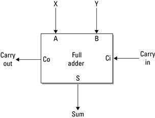
Figure 3.1 Implicit module description of a full adder.
The functional description can be informal, which means its intended behavior is described in comments, exposition, or narrative. This is a very common way of describing a module: someone records the functionality in a manual page or some document or in the implementation as comments. For example, when describing the full adder in narrative we could state:
The full adder component will add three bits together, X, Y and a carry in bit. The addition will result in both sum and carry out bits.
The functional description can also be formal where the behavior is either described mathematically (in terms of sets and functions) or otherwise codified, such as a C subroutine or a behavioral description in VHDL, for example:
– Assign the Sum output signal
S <= A xor B xor Ci;
– Assign the Carry Out output signal
Co <= (A and B) or (A and Ci) or (B and Ci);
Graphically, a module is very simple to denote, it can be as simple as just a box. If we wanted to be more specific, we can give a module a name, which, using a relatively new standard, is shown with a colon (:) followed by the name. In a design, we might want to distinguish between a module (a component in our toolbox) versus an instance (a component being used in a design). Instances (formally defined later) are shown with the module name underlined. Finally, we might want to have multiple instances in our design. If there is no ambiguity, we simply show multiple (underlined) boxes with the same module name, as is seen in Figure 3.2(a). However, if we want to make the distinction clear or if we need to refer to specific instances, we can give them names, illustrated in Figure 3.2(b). This is accomplished by putting a unique, identifying name to the left of the colon and module name.
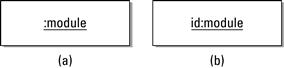
Figure 3.2 Two instances of a module system: (a) the default instance format and (b) the id to give the instance a unique name.
Two more related terms are implementation and instance. An implementation (of a module) is some realization of the module’s intended functionality. Of course, a module may have more than one implementation (just like in VHDL where an entity may have more than one architecture). An instance is use of an implementation. In software, there is generally a one-to-one relationship between an implementation and an instance because the same instance is reused in time. However, in hardware it is common to use multiple copies of an implementation; each copy is an instance. (The verb instantiate means “to make a copy of an instance.”)
Graphically, we distinguish an instance from a simple module by underlining the name in the box. If we want to highlight the fact that there are multiple instances of the same object, we can name the instances by labeling the module with an instance name, colon, module name. For example, Figure 3.2 show two instances of a module. Figure 3.3 is a simple example of four 1-bit full adders being instantiated to produce a 4-bit full adder.
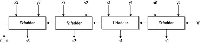
Figure 3.3 Four formally defined modules to generate a 4-bit full adder from 1-bit full adders.
3.1.3 Abstraction and State
Now we are ready to define two major concepts in system design: abstraction and state. These concepts are applied to the modules of a system and are described here. The dictionary defines abstract as an adjective to do with or existing in thought rather than matter (as in abstract art). The verb means to take out of, extract, or remove; in short, to summarize. An abstraction is the act or an artifact of abstracting or taking away; an abstract or visionary idea. Hence, a module is an abstraction of some functionality in a system. We will talk about wanting to make good abstractions — and we’ll discuss the mechanics shortly — but, first, let’s make sure we understand abstraction.
A module is a good abstraction if its interface and description provide some easily understood idea, but its implementation is significantly more complex. In other words, a good abstraction captures all of the salient features of an idea and cuts out all of the details unimportant to realizing the idea.
Our goal in creating abstractions is to overcome the fact that humans can only keep a relatively few number of things in our short-term memory. Typically, psychologists will say that we manage seven items at a time. Individuals will vary but the idea of keeping 100,000s of details on hand in short-term memory is not feasible. So what a good abstraction does is create an uncluttered, coherent picture of the module while shielding us from details that are not immediately relevant. If it is a bad abstraction, it forces us to think not about the module as a single entity, but rather makes us think about how it is implemented. We will see that a good abstraction is also important in reuse.
A great example of how a good abstraction can serve us comes from a subway map. A map of the London subway was first published in 1908. The map was rich in detail: it shows the exact route that the trains take, it is drawn to scale, it shows when the train is above ground, and it even shows rivers and other features.
However, take the perspective of a rider. If I walk up to the map, what am I looking for? Most likely, I want to know what train I need to get on. I am trying to get from point A to point B, and I need to know quickly (before my train departs!) which train I need to hop on. So information such as whether the train travels above ground or below ground doesn’t matter to me. The number of turns a train takes or whether it travels east-west for a while is irrelevant to whether it gets me to point B.
In 1933, the London Underground map was changed. The new map created a bit of stir because a number of people felt like it was less informative. One might ask, what does it hurt to have extra information? The answer is subtle: by abstracting away much of the detail, the map could print the station names in a larger font. By not being true to the relative distances and physical locations of stations, the size of the map could be made smaller. Removing physical features, such as rivers, allowed the train lines to be drawn thicker. The results of these changes make the map much more readable. Functionally trumps literal correctness.
This is the goal of good abstraction: hide the details that do not serve a purpose. If the primary function is to be able to walk up to the map and make a fast decision about which train to get on, then readability is the most important feature. All of the extra information harms this function by distracting the user. So it is with reusable components.
Next, we want to consider another key concept: state. Hardware designers are very familiar with idea of state because it is explicit in the design of sequential machines and we can point to the memory devices (flip-flops) and say, “that’s where the state is stored.” However, in system design, it is a little less concrete because a module’s state is stored in multiple places and in different kinds of memory devices (flip-flops, static RAM, register files, … even off-chip).
Formally, state is a condition of memory. We say something “has state” or is “stateful” if it has the ability to hold information over time. So an abacus and blackboard both have state. A sine wave does not have state. (Note: a sine wave is closely tied to the sense of time and it does not hold information over time.) In general, anything that is (strictly) functional does not have state. Most handheld calculators nowadays have state (they can keep a running total, for example). However, it is possible to build a calculator that does not have state.
Our interest in state has to do with identifying the state in a module. In the mechanics of system design, we will need to separate functionalities into modules, and abstraction and state are going to be major factors in how we derive a module. Because state in a module is not as explicit, the designer needs to consciously identify the states a module can be in and what operations might change that state. In short, good abstraction and careful management of state will lead to good modules and improve the design.
3.1.4 Cohesion and Coupling
The concepts are abstraction and state; the measures are cohesion and coupling. Cohesion is a way of measuring abstraction. If the details inside of a module come together to implement an easily understood function, then the module is said to have cohesion.
Coupling is a measure of how modules of a system are related to one another. A system’s coupling is judged by the number of and types of dependencies between modules. Explicit dependence exists when one module communicates directly with another. For example, if the output signal of module A is the input to another module B, then we say that A and B depend on each other. In software, if A might invoke a function in module B, then we say A depends on B (but B does not necessarily depend on A). The rule for determining dependence is “if a change to module A requires a designer to inspect module B (to see if the change impacts B), then B depends on A.
However, and this is where state comes into play, dependence is not always explicit. Two modules can be dependent in a number of ways. If two modules share state, then there is dependence. For example, if one module uses a large table in a Block RAM to keep track of some number of events and another module will occasionally inspect that table, the latter is dependent of the former. If someone wants to make a change to the format of the table, that change will impact the latter module. This is where explicitly identifying state becomes critical to the formation of modules within a system.
Dependence can crop up in even more subtle ways. Two modules may not have any shared state and may not explicitly communicate via signals or subroutine calls but are dependent. For example, they may be dependent because the system may rely on them completing their tasks at the same time. Hence, the system is coupled in time. Another more esoteric example might be in an embedded system that has sensors and actuators. Two modules may not communicate directly, but if one module is changing an actuator that another module senses, there may be a dependence. Dependence in itself is not bad. Indeed, some dependence is necessary between modules because, we assume, the modules are designed to work together to form the system. What we are interested in is the degree of coupling in the system — that is, the number and type of dependencies.
In general, explicit dependencies that arise from formal interfaces are the best forms of dependence, and a system composed of modules with a unidirectional sequence of dependencies will generally lead to good quality designs. However, if there are many implicit dependencies, circular dependencies (where one module A depends on module B and B depends on module A), or large numbers of dependencies, then chances are the design can be improved.
One way of reducing coupling in a system is through encapsulation. Encapsulation involves manipulating state and introducing formal interfaces. The idea is to move state into a module and make it exclusive (not shared). Often called “information hiding,” it sounds overly secretive, but it is a very effective technique. One consequence is that if one wants to change the module, then there is much more freedom to do things like change the format of the state without the risk of introducing a bug into another module. If the module has good abstraction, then information hiding also allows the module be reimplemented in isolation. All that is necessary is to keep the interface the same.
Coupling is the result of dependencies between modules. Some coupling is inevitable. What kind of system is composed of modules that do not interact at all? The goal here is to avoid coupling when it is unnecessary. A number of techniques will manipulate the degree of coupling. For example, consider the two (very simple) designs in Figure 3.4.
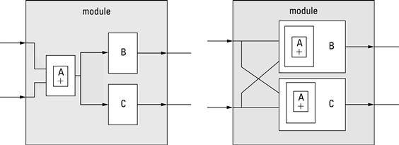
Figure 3.4 (a) Original design and (b) modified design with lower coupling.
In the first design of Figure 3.4(a), the two inputs to the module, x and y, are summed together in submodule A and the results are passed to the submodules B and C. In the second design, the summation is duplicated inside each of the submodules. In the first design, we had two dependencies — submodule B depends on submodule A and submodule C depends on submodule A. In the second design there are no submodule dependencies, so we have clearly reduced the coupling in the design.
What is the advantage? It may be hard to see the advantage in this example because submodule A is so simple and is unlikely to change. However, suppose submodule A was originally designed to work only on unsigned numbers. Over time, it was determined that submodule C also needed to be able to work with signed numbers. So a designer that is looking at modifying submodule C would necessarily have to change both C and A. However, if one changes A, then one must consider the effect on submodule B. Perhaps B will work fine with the change to A. However, the point is that systems with a high degree of coupling have this cascading effect where a simple change cannot be made in isolation. Rather, coupling forces the designer to consider the whole module and understand everything in order to ensure that a change does not break something.
There are two disadvantages to this change. One might argue that we have traded an explicit measure of quality (design size) for a subjective improvement in another measure of quality (maintainability). However, this change does not necessarily increase the design size! In this case, it is entirely possible that submodule A’s functionality will simply merge into the CLBs already allocated by the submodules B and C. Hence, it is possible that there is no net gain in CLBs allocated. Of course, this is not always true and one has to weigh the costs — would the extra CLBs require a larger FPGA?
A second disadvantage to duplicating submodules in order to decrease coupling is that the designer now has to maintain the same component in two places. So if a bug is discovered in submodule A, then it is fixed once in the first design. However, in the alternative design, one has to fix the bug in both submodules B and C. (A word from the trenches: one person’s bug might be another person’s feature. So A may be performing in a way that doesn’t match its description and B requires that it be fixed; however, module C may actually depend on the incorrect behavior to work!)
Wrapping up this discussion, it should be clear that many factors go into applying the design principles described. As this example shows, there are a number of trade-offs for even very simple designs!
3.1.5 Designing for Reuse
In addition to improving design quality, another use of these design principles is to make reusable components. With the increasing complexity of designs, it is in our favor to construct designs with the intention of their reuse. To get started, we must first understand what is necessary to create and identify reusable designs. One indicator is with high cohesion and low coupling, which leads to reusable design components. Note the hidden costs though:
Essentially, RCR says that you have to read the documentation and understand how to use the module before you can reuse it and RCWR says that someone has to put extra effort into designing a module for others to reuse Poulin et al. (1993). For example, when writing a C program to copy data, say 32 bytes of data, we could write our own for-loop to exactly copy the data. We could reuse this loop and possibly generalize it over time (copy words versus bytes, a variable size, or forward versus backward). In contrast, one could learn the “string.h” module in the standard C library. This module provides a rich set of data movement operations. These include operations such as strcpy, strncpy, memcpy, and memmove. The trade-off is learning how to use strcpy versus the time it takes to create your own copying function. In some cases, it could be easier to generate your own in place of learning a potentially complex component. This would suggest that the RCR of the module is fairly high and this discourages reuse. Another cost associated with reuse is RCWR, which is the cost associated with making your custom-created component fully reusable.
One way of managing RCWR is to take an incremental approach: design a specific component for the current design. If it is needed again, copy-and-generalize it. Over several designs, add the generality needed to make it a reusable component.
In VHDL, this can be done through introducing generics into the design. Moreover, one point of doing custom computing machines is to take advantage of specialization! So simply adding generality without leaving the option of generating application-specific versions through generics is counterproductive.
Refactoring is the task of looking at an existing design and rearranging the groupings and hierarchy without changing its functionality. Figure 3.4 illustrates refactoring. Often, it is done to make reusable components. The common use of refactoring is to improve some of the implicit and explicit quality measures mentioned in subsection 3.1.1.
One final word about testing. The value of reusable components is clear. But, of course, there is the danger that components might be refactored and accidentally change their functionality. Regression testing is used to prevent this. It usually is automated and might be simulation driven (à la test benches) or it may be a set of systems that wraps around the component and exercises its functionality. (Multiple systems are needed because one wants to also test all of the generics that are set at compile-time.)
3.2 Control Flow Graph
Throughout the text we use the idea of a software reference design. There are many ways to represent a system — from formal specifications to informal (but common) requirements, specification, and design documents to modeling languages such as UML. In addition to these representations, it is often common for a designer to build a rapid prototype — a piece of software that functionally mimics the behavior of the whole system, even hardware modules that have not been implemented yet. We refer to this software prototype as the software reference design. The major drawback of software reference design is the cost associated with creating it but, as a specification of the system, it has a number of advantages. The first is that it is generally a complete specification. (If there is any question about how the future system is to behave, one can observe how it behaves in the reference design.) Another advantage is that it is executable — a designer can gather valuable performance data from running the software reference design with specific input data sets. Finally, because the software reference design is computer readable, the specification can be analyzed by existing software tools.
Through the next several chapters we will assume that a software reference design exists. Here we show how computation in software reference design can be represented mathematically. The next chapter uses this notation to help make decisions about what parts of the system should be implemented in hardware versus software.
We do this by borrowing some concepts from compiler technology — primarily the control flow graph. The control flow graph summarizes all possible paths of program from start to finish in a single, static data structure. Formally, a Control Flow Graph (CFG) is graph ![]() where the vertices (or nodes) V of the graph are basic blocks and the directed edges indicate all possible paths that program could take at run time. A basic block is a maximal sequence of sequential instructions with a Single Entry and Single Exit (SESE) point. Figure 3.5 illustrates this definition. The first group of instructions (A) is not a basic block because it is not maximal — the first instruction (store word with update) should be included. The second group of instructions (B) is a basic block. The last group (C) is not a basic block because there are two places to enter the block (at the store word instruction after the add immediate, or by branching to label .L2).
where the vertices (or nodes) V of the graph are basic blocks and the directed edges indicate all possible paths that program could take at run time. A basic block is a maximal sequence of sequential instructions with a Single Entry and Single Exit (SESE) point. Figure 3.5 illustrates this definition. The first group of instructions (A) is not a basic block because it is not maximal — the first instruction (store word with update) should be included. The second group of instructions (B) is a basic block. The last group (C) is not a basic block because there are two places to enter the block (at the store word instruction after the add immediate, or by branching to label .L2).
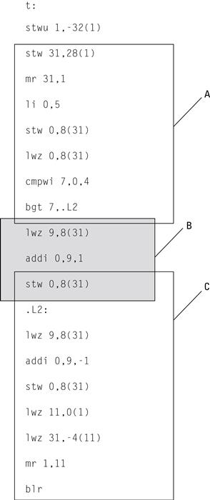
Figure 3.5 Groups of instructions; (A) and (C) are not basic blocks, (B) is a basic block.
An edge (b1, b2) in a control flow graph indicates that after executing basic block b1 the processor may immediately proceed to execute basic block b2. If the basic block ends with a conditional branch, there are two edges leaving the basic block. If it does not end with a branch or if the last instruction is an unconditional branch, there will be a single edge out. Two special vertices in the graph, called Entry and Exit, are always added to the set of basic blocks. They designate the initial starting and stopping points, respectively.
Informally, a basic block sequence of instructions that we know, by definition, will be executed as a unit. The edges in the CFG show all the potential sequences in which these units are executed. For example, the simple subroutine shown in Figure 3.6(a) has identified the basic blocks in a C program. In Figure 3.6(b), the C program has been compiled to PowerPC assembler code and the basic blocks have been identified. Finally, the control flow graph is illustrated in Figure 3.6(c). Note that it is possible to identify the basic blocks in a C file if one knows how the compiler emits assembly code. Unless it is obvious, we use assembly code to illustrate basic blocks.
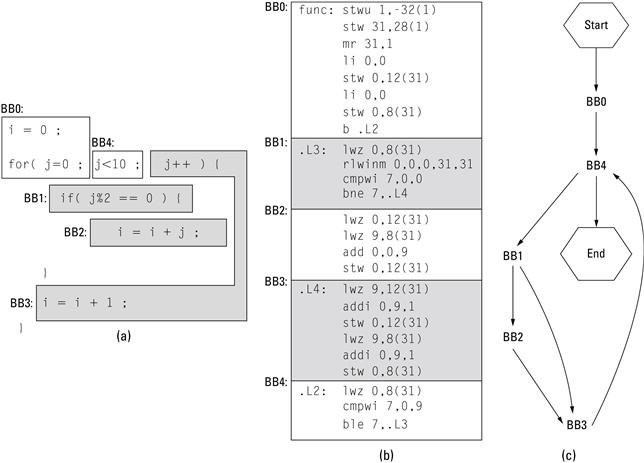
Figure 3.6 Basic blocks in (a) C source code (b) translated to assembly (c) a control flow graph.
Compiler researchers and developers use the control flow graph in a number of ways. Often, graph algorithms applied to the CFG will result in a set of properties that guide transformations (optimizations) designed to improve the performance of the program. When combined with data dependence (see Chapter 5) the CFG can be used to determine what parts of the program can be executed in parallel (and thus implemented spatially in hardware). For now, our immediate need is to visualize the software reference design. The next chapter uses the basic blocks as the atomic unit that can be partitioned between hardware and software.
3.3 Hardware Design
Thus far, the discussion of system design has been high level and general. Next we turn toward hardware design and, very specifi-cally, the hardware components available to the Platform FPGA designer. We begin with a brief description about how these common architectural components evolved and then describe several of the broad classes of hardware modules available. This section ends with a general description of how the designer can expand their toolbox with custom hardware modules.
3.3.1 Origins of Platform FPGA Designs
Simply put, designers rarely want to build an embedded system from scratch. To be productive, an embedded systems designer will typically begin with an existing architecture, remove the unneeded components, and then add cores to meet the project requirements. The processor-memory model, seen in Figure 3.7, which is basic desktop PC architecture, has worked well as a starting point. To begin, we briefly review some key computer architecture components so we are able to understand and use them in our Platform FPGA designs.
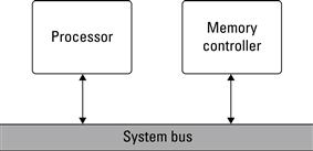
Figure 3.7 The fundamental process-memory model to be used as a base system in Platform FPGA designs.
The introduction of the IBM Personal Computer (PC) in 1980 had an enormous impact on the practice of building computing machines. The intent was to make a system that would appeal to consumers and hobbyists alike; therefore, low-level details of the system were readily available. This spurred third-party development of peripherals and (probably unintentionally) compatible machines from other manufacturers. As the speed of the microprocessor, volume of machines, and competition increased, the cost actually decreased. It became possible for manufacturers and vendors to try different computer architecture designs. Ultimately, the architecture that has evolved is what is common in today’s desktop computers.
Later computers use a two-bus system where the processor and memory reside on a processor-specific system bus and the lower speed peripherals (serial ports, printers, video monitor) reside on a generic, standard peripheral bus. Figure 3.8 shows this arrangement, which allows the system components to evolve rapidly in terms of clock frequencies, voltages, and so on while maintaining compatibility with the third-party peripherals, which do not change as quickly.
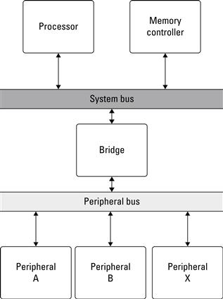
Figure 3.8 The two bus process-memory model used to support parallel, independent high-speed and low-speed communication.
Embedded computing architectures have not changed much from this basic arrangement; in fact, this foundation has allowed designers to focus on improving the individual components. The bus model is arguably insufficient for certain application needs, but it serves the needs of general applications well. This organization makes a good starting point for our designs with Platform FPGAs. We can utilize the hard or soft processor core(s), on-chip memory and off-chip memory controllers, and peripherals to support system input and output to build a base system that resembles these computer organizations.
Platform FPGAs have adopted these two basic processor-memory model from the desktop computer architecture because it provides an established framework that can be built upon for custom designs. With the addition of existing components and cores, more complex systems can be constructed, often within a considerably shorter time frame than traditional embedded systems designs. In fact, in section 3.A you already assembled a simple Platform FPGA system when building the “hello world” FPGA example. Within this section we aim to go into more detail on what comprises a Platform FPGA base design (system). We use the the basic computer organization processor-memory model and expand on it to work up to a useful base system.
A valid question to ask at this point is “why create a generic base system when we are using FPGAs?” FPGAs by their very nature are programmable and application specific. In an ideal world where a designer’s time could be infinitely spent on the project, there were no deadlines, and money was no object, creating completely custom designs would make sense. Unfortunately, the ever-growing demand for first-to-market solutions requires designs to be up and running and brought to market quickly. FPGAs offer an additional advantage of providing field programmability to the mix, allowing a potentially less than ideal solution being initially offered, then updated in later revisions.
3.3.2 Platform FPGA Components
Chapter 2 discussed the components that exist in an FPGA, such as logic cells, blocks, and on-chip memory. While these components are useful in all FPGA designs, they will be the building blocks for much larger systems. With the ideas of modularity, cohesion, and coupling of components and designs, we want to begin to build base systems that can be used and reused as a starting point for embedded systems design. We have already discussed the strengths of this approach and introduced the prevalent organization with the processor-memory model. Because each design is different, it is obvious that the design will require modifications, but the processor is a good place to start.
Processor
Generally speaking, the processor offers the designer control and a familiar design environment. Even if the final design will require little or no involvement from the processor, its use within the rapid prototyping or early development stages can help rapidly evolve the design. For us, the processor is an obvious starting point when describing and building a processor-memory model design. In a Platform FPGA, two types of processors can exist, hard and soft core processors. Chapter 2 discussed the hard processor cores in detail and even gave examples of PowerPC 440 integrated in the FPGA fabric on the Xilinx Virtex 5 FX series FPGAs.
Other Platform FPGAs provide sufficient reconfigurable resou-rces that a soft processor core can be implemented in the logic blocks and surrounding resources of the FPGA. Soft processors offer a great deal of flexibility, as they are by their very nature configurable. Unlike hard processors, where functions have been fixed since fabrication, incremental improvements to a soft processor (such as the more recent addition of the memory management unit to the Xilinx MicroBlaze processor) provide the designer with a more flexible design approach.
While this could quickly turn into a long discussion on the advantages and disadvantages of processors in hardware versus software, we focus instead on the processor’s capabilities. For instance, even the most basic processors, requiring a minimal amount of resources (i.e., PicoBlaze), can operate in what is called stand-alone mode, offering only the most basic functionality (such as stdin/stdout). More advanced processors may include memory management units (MMU) to support more verbose operating systems (such as Linux). There are even processors that offer coherency with shared memory between multiple processors to create a multicore processor (similar to what exists in commodity desktop PCs).
Overall, knowing the processor’s role in the application can help dictate which processors can and cannot be used. For instance, the PicoBlaze is well suited for more complex state machines, but not for running Linux. Likewise, soft processors may offer wider flexibility when migrating from one FPGA device family to another (or even to a different FPGA vendor). Before choosing which processor will be the cornerstone of the design, consider the following questions:
• Does the FPGA include hard processors?
• Are there sufficient resources to implement a soft processor?
• What role will the processor play in your design?
• What type of software will be used on the processor?
• How much time will the processor be used versus hard cores?
Some of these questions may be easier to answer than others, but being able to address them before moving too far along the design process is important. Chapter 4 helps address questions regarding identifying suitable functions to be implemented in hardware versus software. This chapter is more concerned with construction of the platform and augmenting it to meet the design’s needs. If the FPGA does include a hard processor core(s), the initial design might be best suited to include its use rather than expend additional resources on a soft processor. If, however future generations of the system will include different FPGAs, it might make more sense to use a soft processor core that can be moved between FPGAs with as little effort as possible. Vendors and developers of soft cores should be able to provide enough information for a design to determine if it is feasible to include in the chosen FPGA.
Memory
In order for the processor to do any useful work, memory must be included to store operations and data. Different computer organizations and memory hierarchies could be discussed at this point. Whether the processor follows the Von Neumann or Harvard architecture or contains levels 1, 2, and 3 cache is arguably too low level for embedded systems designers. Instead, we focus on the following questions:
• What type of memory is available?
• Is there on-chip and/or off-chip memory?
• How much on-chip/off-chip memory is available?
• Is the memory volatile or nonvolatile?
• How does the processor interface with the memory?
• How does the system interface with memory?
As mentioned in Chapter 2, modern FPGAs include varying amounts of on-chip memory (often referred to as block RAM). The uses of this memory are wide and varied based on the application. The memory can be included within a component, core, or as part of the base system. The location of the memory dictates its interface and accessibility. For example, say a custom core includes a FIFO built from on-chip memory, it may have a standard FIFO interface (enqueue/dequeue), which only the custom core can access, or it may be accessible to a processor as a way of loading data into the custom core to be operated on (such as a single precision floating point addition core). When designing systems with on-chip memory needs, it is important to identify how it will be used within the system.
In the event the design requires more memory than is available on-chip, off-chip memory is required. There are many different forms of off-chip memory and knowing which type to use is a difficult decision that goes beyond the scope of this chapter. However, interfacing with the particular memory is important to address now. A memory controller is required to handle memory transactions, requests for access to memory in order to read or write data from a specific address. The memory controller is a soft core that can be configured to meet the specific needs of the memory it is interfacing with. For example, each DDR2 DIMM has specific operational characteristics that require complex state machines to interface with it. Fortunately, for the designer, many of these memory controllers have already been designed with generic parameters to allow for quick integration with different memory manufacturers. Within FPGA designs it is possible to include processor-centric memory access, where the processor issues all requests on behalf of the system, or to include Direct Memory Access (DMA), where cores within the system can request memory directly.
For both on-chip and off-chip memory it is difficult to provide strict design rules, as they can be used in such a variety of ways. However, utilizing them efficiently is of critical importance because the rate at which memory is increasing lags behind the processor Wulf & McKee (1995), and with the addition of multiple sources contending for a single resource, this demand for memory only further exacerbates the problem. Chapter 6 covers how to tackle memory bandwidth management questions more efficiently. Of key importance is configuring the system to tightly integrate the components needing low-latency access to memory and separating them from components that may not access memory as frequently or at all.
Buses
Now that we have described the two main components in a processor-memory model design, we must start to address the various ways to connect them. The simplest approach (beyond a strict point-to-point interface) is to provide a bus. The processor(s) and memory controller(s) connect to the bus via a standard bus interface. The bus interface is specific to the particular bus, but at the simplest level consists of address, data, read/write requests, and acknowledgment signals. The bus also includes a bus arbiter, which controls access to the bus. When a core needs to communicate with another core on the bus, it issues its request for access to the bus. Based on the current state of the bus, the arbiter will either grant access or deny access, causing the core to reissue its request. A core that can request access to the bus is considered a bus master. Not all cores need to be bus masters; in fact, many custom cores are created as bus slaves, which only respond to bus transactions.
A bus on an FPGA is implemented within the configurable logic, making it a soft core. For example, Xilinx uses IBM’s CoreConnect library of buses, arbiters, and bridges. More details regarding the CoreConnect library are presented in section 3.A. Some important design considerations need to be addressed when using buses.
• What cores will need to directly communicate?
• Do certain cores communicate more often than others?
• Do specific cores require a higher bandwidth between them?
As mentioned earlier, it is common to find a two-bus system in desktop computers. This is done to isolate the lower speed peripheral devices from higher speed devices (such as the processor and memory). In system design, it may be advantageous to put certain cores on one bus and others on a separate bus. By adding a bridge between the two buses, it is possible for cores to still communicate, although at the cost of additional latency.
System Bus
In multiple bus designs the bus with the highest bandwidth that connects the processor, memory controller, and remaining high-speed devices (such as a network controller) together is often referred to as the system bus. Xilinx uses IBM CoreConnect’s Processor Local Bus (PLB) as its equivalent system bus. When the number of cores needing access to the bus is relatively small, connecting all of the cores on a single bus is a logical, resource-efficient decision. In Platform FPGA designs, the system bus is the fundamental mechanism to communicate between the processor and custom hardware core. As the number of hardware cores grows, a decision must be made as how to most efficiently support these additional cores in combination with the already existing system. One solution is to introduce a second bus.
Peripheral Bus
A second bus may be added to separate the design into different domains. In some cases this is done for high-speed and low-speed designs. In others, it may be to provide a subset of the cores with a dedicated bandwidth for communication. In either event, addition of a second bus, often known as the peripheral bus, allows two arbiters to control communication across the two buses. With a single bus, if the processor was accessing data from the memory controller, any other cores needing to communicate would be required to wait for the memory transaction to complete. In a two-bus system, those cores could be migrated to the peripheral bus and allowed to communicate in parallel.
Bridges
In some cases it is necessary for a core on the system bus to communicate with a core on the peripheral bus. This requires the addition of a bridge. A bridge is a special core that resides on both buses and propagates requests from one bus to another. A bridge functions by interfacing as a bus master on one bus and a bus slave on the other. The slave side responds to requests that must be passed along to the other bus. The master side issues those requests on behalf of the original sender. Sometimes only a single bridge is required; if the peripheral bus only will respond to requests from the system bus, a system-to-peripheral bridge is required. However, if cores on the peripheral bus need access to the system bus (say for access to the off-chip memory controller), then a second bridge, a peripheral-to-system bridge, is required. The common nomenclature for describing the interfaces of a bus in terms of master side and slave side is as follows. The system-to-peripheral bridge means that the bridge is a slave on the system bus and a master on the peripheral bus. This may seem backward, but the reason is quite simple. In order to communicate from the system bus to cores on the peripheral bus, the bridge must respond to system bus requests (making it a slave on the system bus) and issue the request on the peripheral bus (making it a master on the peripheral bus).
Peripherals
Now that we have established a mechanism to connect cores together we should address some of the peripherals a system designer may add to a design. When we talk about peripheral cores, we usually are referring to hardware cores that interface to peripheral devices, such as printers, GPS devices, and LCD displays. Peripherals themselves are traditionally the components around the central processing unit. In our case, some peripherals (such as a video graphics adapter) may be entirely implemented in the FPGA, but often the peripheral is external to the FPGA and the hardware core provides the interface.
In Chapter 7, we dedicate the whole chapter to interfacing with the outside world. Here we simply mention common peripherals found in Platform FPGA designs.
A number of high-speed communication cores have been implemented as FPGA cores. There is a PCI Bridge and a PCI Arbiter — the former is needed to connect the FPGA’s system bus to an existing full-function PCI bus, whereas the latter includes the logic to create a full-function PCI bus. A variety of Ethernet cores are available for connecting the Platform FPGA to a (wired) Ethernet network. Likewise, a variety of USB cores provide support for different versions and capabilities. Many of the older (low-speed) communication cores have been implemented as well, including UARTs, I2C, and SPI.
As part of the principles of system design, building cores for reuse leads to the eventual accumulation of a library or repository of cores. These cores may provide functionality that many of the base systems need. For example, more and more cores are requiring Internet access whether it be for debugging purposes or to update an embedded system’s database; having a core that can be integrated quickly into a design that has been tested previously reduces design time significantly.
Building Base Systems
Enough talk, it is time to put these concepts together and build a simple base system, consisting of a process, on-chip memory, off-chip memory, and a UART for serial communication with a host PC. We are being a little generic still in terms of the actual core, but in section 3.A we will be more specific with respect to Xilinx FPGAs. Still, we have a processor, two types of memory, and a UART. We have yet to mention what would be used to connect these components together because that is a little more application specific. In some cases it makes sense to separate the high-speed and low-speed devices onto different buses.
In this example, there would be no immediate need for such a separation. Remember that this is the base system from which larger designs will be built. As a result we want to be flexible enough in our design to allow custom cores to be added without requiring significant changes to this base system. For that fact, we will include both a system bus and a peripheral bus. Figure 3.9 depicts this initial base system. Notice that with the addition of buses, we need to include a bridge. Because the UART is a slave on the peripheral bus, there is no requirement for adding a second bridge to allow it to master the system bus. If future designs require this, we can go back and add the peripheral-to-system bridge.
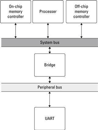
Figure 3.9 Block diagram of the base system consisting of a processor, on-chip and off-chip memory, and a UART.
While drawing boxes suffices for an academic approach, it is insufficient for practical implementations. We would not build this base system with schematic capture software because the number of signals and wires to connect would be enormous. Instead, we use hardware description languages. Using the bottom-up design approach, we could create a single HDL file and instantiate each of the components within it.
Not only do we need to connect all of the components input/output signals, we need to connect the input/output signals that go off-chip. For example, the UART includes transmit and receive pins that are routed off-chip to a RS232 IC to provide serial communication between the FPGA and the outside world. This requires additional constraints to be set to notify the synthesis tool that a signal is to be routed to a specific pad and pin.
In practice, even this amount of work is inefficient. FPGA and software tool vendors provide GUIs or wizards to help automate this process. For the beginning designer, the tools are a great starting point because they help the designer identify key components and how they are connected. For the more experienced designer, the tools and wizards may prove to be less useful.
3.3.3 Adding to Platform FPGA Systems
Now that we have a base system, let’s go ahead and add some custom compute cores. Many embedded systems devices are now including some form of network interface, whether it be wired or wireless. For demonstration purposes, we will add a TCP/IP 10/100/1000 Mbit Ethernet network core. The network core will provide us with access to the FPGA from anywhere in the globe via a Web interface. Adding this core to the base system can be as simple as adding the instance to the top-level HDL file and updating the pin constraints file. We will add the network core to the system bus because as data are transferred to and from the FPGA, we will use the off-chip memory as a temporary storage buffer. Figure 3.10 is the modified block diagram of this base system. In addition to networking, we have also connected a USB and I2C interface to the peripheral bus just to start to round out the theoretical design.
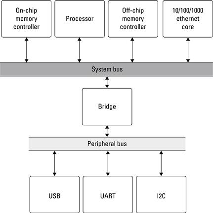
Figure 3.10 Block diagram of the base system with the additional cores: networking, USB, and I2C.
The benefit of using the bus (or two-bus) within the design is it allows the system to be modified (adding or removing cores) with ease. As long as the new core has the same bus interface, typically a standard such as the PLB that is published and widely available, a systems designer just needs to connect up the signals. In the event that the new core is a slave on the bus, the new core will need to be assigned a unique address range from the system’s address map. The address range is how other cores on the bus will communicate with the new core.
Address Space
From a hardware perspective, the “location” of data is straightforward and easily identifiable. Off-chip memory is physically located outside of the FPGA’s packaging, typically as a separate memory module or, more commonly, as a Dual In-line Memory Module (DIMM). From a design perspective, accessing the memory is nothing more than through the memory’s address space. Off-chip memory may be addressable from the address range 0x30000000–0x3FFFFFFF, for a total of 256 MB of addressable data. Globally addressable on-chip memory, located on the same bus as the off-chip memory controller, may have an address range 0xFFFF0000–0xFFFFFFFF, for a total of 64 KB of addressable data. In Platform FPGA designs it is possible to automatically generate these address ranges or to set specific address ranges.
For on-chip memory that is only local to a compute core, the address range is user defined and commonly word addressable (instead of byte addressable). The address range is also important for any compute cores that must communicate with the processor. We mention this information here because up until now we have not interacted with a range of compute cores or memory. Figure 3.11 shows that address map for the two-bus base system mentioned previously. Each core that has an address range is at least a slave on the bus. The processor is a bus master only and therefore does not include an address range within the address map.
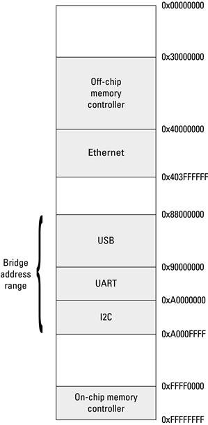
Figure 3.11 One possible address map for the theoretical two-bus system with networking, USB, I2C, and UART.
In the two-bus system, the bridge acts as a middleman between requests issued from the system bus to the peripheral bus. The bridge must be assigned an address range that will span all of the cores on the peripheral bus. If the bridge is given the incorrect address range, requests may never make it to the peripheral bus or to the destination hardware core.
3.3.4 Assembling Custom Compute Cores
In Chapter 2, hardware description languages were introduced with a few examples to help the reader grasp some of the concepts. We also covered how to use existing tools and wizards to create components and custom core templates. Now it is time to cover how to design and assemble custom compute cores. While there is a large body of writing on how to design digital computing systems, both manually and automatically, we look at the process from a more systematic engineering approach. To start, we want to answer the age-old question of “why build custom compute cores?” Once answered we discuss design approaches, consider design rules and guidelines, look at how to test and debug hardware, and finally culminate with a functional custom core.
Why Build Custom Cores?
We begin with the most important question, “why build custom cores?” It is widely believed that hardware development is difficult and because there are more software professionals in the workforce than there are hardware engineers, some might argue to use processors and build software. Furthermore, processors are inexpensive and cost-effective, and processor manufacturers put an enormous amount of design effort into a piece of hardware that will ship many millions of units over its lifetime.
Often, the immediate response to the question “why design hardware?” is “for performance” and by performance the speaker typically means “speed.” This is true; however, there are other compelling reasons to implement hardware as well. These include computational efficiency and predictability. We’ll look at each of these reasons in detail because it is important for a hardware designer to know when a hardware solution is and is not justified.
Advantage: Speed
Because custom hardware designs are often used to speed up applications, some designers will occasionally make the mistake of generalizing that “hardware is faster than software.” However, the idea that hardware is faster than software is a fallacy. In fact, if naively implemented, hardware is often slower than software. Moreover, it is true that any hardware design implemented in an FPGA will perform 5× to 10× slower (and consumes more area on a chip) than the same circuit implemented directly in silicon (using the equivalent process technology). If the design we happen to implement is similar to a processor, then we gain nothing and lose much in speed (and area). So how does FPGA hardware outperform a processor?
Practically speaking, there are two reasons why some FPGA designs have a performance advantage plus a couple of minor reasons. The first practical advantage is rooted in the execution model. The sequential computing model of the standard von Neumann processor creates an artificial barrier to performance by expressing the task as a set of serial operations. With hardware, the task’s inherent parallelism can be expressed directly. To compensate for its inherently serial operation, modern processors commit a significant portion of the hardware resources to extracting the instruction-level parallelism to increase their speed, which we will revisit shortly when we discuss efficiency. Although less significant overall, another way that the execution model can impede performance is in instruction processing. The processor model has to commit resources to fetching, decoding, and dispatching instructions, all of which are functionality that is commonly part of the hardware design. For some applications, memory bandwidth limits the performance and part of the bandwidth is consumed by instructions being fetched from memory. In hardware designs, the instructions are implicitly part of the design.
The second practical reason FPGAs have been able to outperform standard processors has to do with specialization. In general-purpose processors, data paths and operation sizes are organized around general requirements. This typically means 32- or 64-bit buses and functional units. Thus, to multiply an integer by some constant c requires a full-sized multiplier in a processor. However, if additional information about the application is known, an FPGA-based implementation can be created with customized function units to meet the exact needs of the application. For example, a constant multiplier can be orders of magnitude faster than a general-purpose multiplier.
Although, run-time reconfiguration is possible, it is currently not in widespread use. Nonetheless, FPGAs can use this technique to outperform a general-purpose processor by using information only available at run time to produce specialized circuits. For example, a circuit that computes Triple-DES (an encryption algorithm) can be several orders of magnitude faster if the key is known in advance. This particular example has been demonstrated elsewhere Hennessy & Patterson (2002). Unfortunately, building run-time reconfigurable designs is a challenging, time-consuming process. Until design tools and methodologies mature and become easier to use, it is unlikely that this important source of improved performance will become common. The final chapter discusses run-time reconfiguration in more detail.
Advantage: Efficiency
Suppose a hardware implementation of task A takes exactly the same amount of time to complete as the equivalent task executed on a processor. We can assume that the software implementation is easier to develop. Is there any reason to build a hardware implementation? The answer is yes when the hardware solution is more efficient. By efficiency, what we are concerned with is how to accomplish a fixed task with a variable amount of resources. By resources, we could be talking about area on a chip, the number of discrete chips, or the cost of the solution. While speed is a predominant reason to commit to a hardware design, efficiency is still a valid reason. A hardware design plus a processor is often more efficient than two processors.
For example, suppose we have a network interface that implements a standard protocol (such as TCP/IP over Ethernet). If we needed to augment an existing computer (that is already loaded to its capacity) to handle network events, then the two options might include adding another processor dedicated to network traffic and building a custom network interface that offloads the network tasks. If both approaches meet the minimum criteria, then we say the more efficient solution is the one with a lower cost. If the system is being deployed on a single chip, then the more efficient solution is the one that uses less area.
Advantage: Predictability
While efficiency is an important consideration, it is often the case that a processor is not being used to its full capacity. Thus, someone might argue that the processor can simply multitask in new functionality. Even if this does not overload the processor, there is another compelling reason to use a hardware implementation. This case arises in embedded systems where timing constraints are very important. When there are real-time demands on the system, scheduling becomes important. Hardware designs have the benefit of being very predictable, which in turn makes scheduling easier.
So, there are cases when it makes sense to move a task to hardware if it makes that task more predictable or if it makes scheduling tasks on the processor easier. For real-time systems, where the goal is to satisfy all of the constraints, predictability is often more valuable than simply making the system faster.
Disadvantages
Perhaps the biggest disadvantage to building hardware solutions is one already mentioned, the development effort required. Compared to the numbers of professionals that can code software, there is a small number of hardware designers. Moreover, most people will assert that designing hardware is more difficult than coding software. Certainly, for large designers, there are more details that one has to attend to. So, unless there is a compelling reason (in terms of the performance metrics from Chapter 1 or the advantages just mentioned), then it may not be worth the extra effort. A second disadvantage is the loss of generality. It is simply the nature of our modern world that product requirements will evolve over time. The loss of generality has the potential of negatively impacting the design over time.
In summary, Platform FPGAs offer speed, efficiency, and predictability advantages over software-only solutions — compelling advantages for many emerging embedded computing system projects. However, there is no universal answer to the question. As a Platform FPGA designer, part of your task includes determining when a simple microcontroller is appropriate.
Design Composition
In general, there are two ways of building digital computing machines. The first is the one that has been traditionally covered in most sophomore-level digital logic courses, which begins with logic gates. The second, which is sometimes covered in later courses, starts with higher level logic blocks from which complex systems are composed.
In the first approach, the designer begins with requirements that are translated into a specification (expressed in various forms such as Boolean expressions, truth tables, and finite state machines). From there, all of the various formal techniques are used to reduce the number of states, minimize the Boolean functions, and realize the machine in the fewest number of components. When we say “built from gates” this is the approach we are talking about.
In the second approach, the designer starts with logic blocks that have a predetermined functionality — such as decoders, n-to-1 multiplexers, and flip-flops. These components are selected by the designer and are arranged creatively to meet the requirements. Logic gates may be used but their need is diminished by the functionality provided by the other components. The second approach is what we will focus on for the remainder of this book. There are many reasons to use the first approach; however, for practical designs utilizing millions of gates, maintaining the design becomes a daunting task that is simplified by a more modular design approach.
Generally speaking, there are three steps when designing modular custom cores. The first step is to identify the inputs and outputs of the core. In some designs the inputs and outputs are already set based on the functionality of the system. For example, in a bus-based system the inputs and outputs are initially fixed to at least the bus signals. Additional signals may be added based on the design (i.e., connecting an interrupt signal from the core to the processor). These signals may change through the design process, but establishing a solid interface to a top-level component will greatly assist in not only the component’s composition, but aid in the design of any components that eventually will use this core.
The second step is to identify the operations and compose a data path, usually a collection of multistage computations (i.e., a pipeline). Each component is designed with a particular function in mind. The exact operations needed may not be as clear during the beginning of the design phase, but determining the necessary low-level functionality (or subcomponents) allows for the construction of a data path. The data path represents the flow of data through the component. Once the flow has been established it becomes possible to construct a computation pipeline. A pipeline in hardware contributes to the performance and efficiency of the design. Capturing the stages of the pipeline may initially be difficult, but starting a design with the concept of supporting pipeline operations makes the process much more manageable.
The third step is to develop a controlling circuit that sequences the operations, usually a finite state machine. We often think of hardware in terms of parallelism, that is, independent operations that can be executed at the same time. Parallelism is one of the keys to achieving speedup over processor-based designs. However, many designs still require computations in some sequential flow. Consider a simple equation:
![]()
It is possible to build hardware to multiply x*y in parallel with the multiplication of 4*z, but addition of the two results must wait for completion of the multiplication. A finite state machine can be used to control the computation by first performing the two independent (parallel) multiplications and then performing the addition.
Bottom-Up and Top-Down Design
Earlier we mentioned two design approaches, bottom up and top down. In many FPGA designs, the bottom-up approach is used when assembling systems, as described previously. This same approach can be used for assembling custom compute cores. For example, when using the structural HDL method, each component is built by instantiating subcomponents. Before the top-level design can be completed, each of the subcomponents must be designed and tested. In this approach, modularity and designing for reuse are very important.
In the bottom-up approach, each subcomponent can be treated as a black box, where only inputs and outputs are known to the designer. The underlying functionality may be represented in a data sheet with definitions of latency, throughput, or expected outputs. In fact, designs are often completed by more than one person. As a result, each designer relies on a black box that will be filled in later by another designer.
Alternatively, starting from the top-level design and working down to low-level components is known as top-down design. When designing custom compute cores, the designer would begin with the core’s interface (inputs and outputs). This creates a black box representation of the core. Once the interface is set, the designer can begin to systematically decompose the design into its subcomponents. This process is repeated for each subcomponent until low-level components are identified to be simple enough to design. The top-down approach does not necessarily associate with behavioral or structural HDL, but a designer may use more behavioral HDL.
The end product of either a top-down or a bottom-up app-roach should result in the same functionality. Internally, the design may look drastically different, but the top-level interface and operation should perform identically based on the specification.
Let’s work with an example to illustrate the different ways components can be combined to form large modules. Consider the simple system illustrated in Figure 3.12. The desired functionality is to add four numbers together.
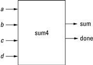
Figure 3.12 The top-level component to add four numbers.
Beginning with a familiar approach, we consider the temporal implementation shown in Figure 3.13. While this implementation may not be immediately comparable to a software solution, consider how sequential addition is performed. In this solution, four numbers (a, b, c, d) are connected to a multiplexer, which is controlled from a simple state machine. The state machine increments from 0 to 3 to select each of the four inputs. The multiplexer feeds each input to the arithmetic logic unit (ALU), which is set to add mode. The ALU stores the result in a register, and the state machine increments the state bits s1 s0 to add the next input. In this approach, the addition would take four additions:
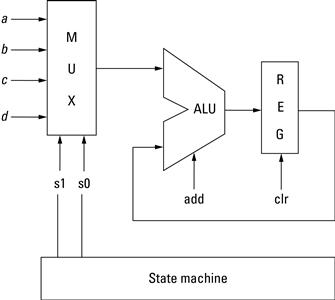
Figure 3.13 A temporal implementation.
In a system were only one ALU and register exist, this would be a sufficient minimal resource solution. Furthermore, augmenting this design to add eight numbers instead of four would only require a large multiplexer and addition state bit s2.
Clearly this is not the fastest approach. In terms of speed it is desirable to perform as many independent operations in parallel as possible. Unfortunately, there is a cost with parallel approaches, that is, added resources. Using three ALUs we could perform temp1 = a + b and temp2 = b + c in parallel and then add temp1 + temp2. The trade-off between latency and resources is ultimately at the hands of the designer, but it is wise to consider both low latency and low resource utilization approaches early in the design phase in case there is a need to switch between the two in a later phase.
Spatial Composition
Most programmers are familiar with the typical sequential composition rules of a von Neumann compute model. The simplest rule — two operations are sequenced — implies that there is a thread of control where the second operation takes place after the first computes its result. This is a degenerate case of spatial composition, which relaxes the strict ordering of operations. Hardware designs are not limited to sequential execution (unless dictated by the design). Thus, when a hardware designer specifies two operations, they will execute simultaneously unless the designer further specifies an ordering. Figure 3.14 shows a spatial implementation of the four adder example. In this case, the additions are pipelined such that results are fed forward to the next adder.
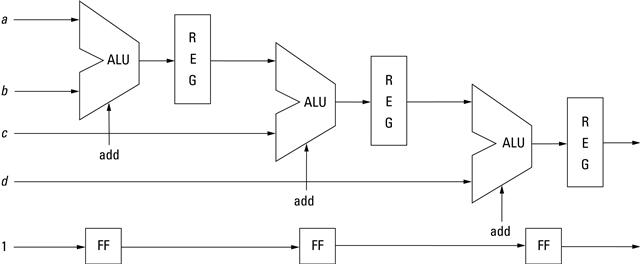
Figure 3.14 A spatial implementation.
The loose ordering of operations in time is both a boon and a bane for Platform FPGA design. Concurrency is what gives system designers speed, and control of timing is what gives system designers predictability — both primary motivations for using hardware. However, simply expressing timing relationships between operations is a challenge, let alone determining what the correct timing relationships are. Consequently, this is a frequent source of system design errors. Chapter 5 goes into more detail regarding spatial design.
3.4 Software Design
Embedded system products have rapidly become more sophisticated in recent years. In the past, software was simple, had a single task, and played a relatively minor role compared to the design of the hardware. If two tasks were needed, they were often kept independent — logically and physically. As microcontrollers increased in speed, embedded systems added system software to manage multiple threads of control. This allowed a single microcontroller to time-multiplex separate tasks. Nowadays, some embedded system processors have memory management units, support virtual memory, and are fast enough to support full, modern operating systems. This has been a boon for users because it resulted in an explosion of product features. With a full-featured operating system, embedded systems designers can incorporate or adapt large software applications that were originally written for general-purpose desktop or server machines. This section aims to cover the various background information to help embedded systems designers understand and implement complex system software in Platform FPGA-based systems. We cover specific design and tool flows in section 3.A with the end result being running a complete Linux system on the Xilinx ML-510 development board. Here we address the concepts and definitions.
3.4.1 System Software Options
Just as with hardware, an embedded systems designer has a wide range of choices when it comes to system software. By system software, we are referring to any software that assists the application — usually by adding a software interface to access the hardware. This ranges from a simple library of routines to a full-fledged operating system that virtualizes the hardware for individual processes.
In the simplest situations, almost no system software is needed at all. In this case, the C start-up files (subroutines that the compiler/linker adds to every C program) are modified. At run time, these subroutines execute before calling the main function of the designer’s application. With no operating system, these initial subroutines are responsible for setting up the processor and peripherals. (There is a collection of files with names such as crt1.o, crti.o, and gcrt1.o. The CRT part stands for C run time and, depending on the compiler options, different variants of the start-up files are used. Also, different processors will have different start-up files and the names may vary as well.) Even if the processor has a memory management unit, simple cases such as this execute the application in “real” or “privileged” mode and no memory protection is used. This is called a standalone C program because it runs without the support of any additional system software. In addition to being simple, an advantage of this approach is that there is essentially no overhead.
For Platform FPGAs, this is often a first step when testing new hardware cores because the C program typically has complete access to the hardware, it is very simple to compile a small test program, and there are fewer steps to test a live system. Often, this solution produces a small enough executable that the entire software system (application and system software) can fit within the block RAMs of the Platform FPGA. Avoiding off-chip RAM can be a significant advantage for some embedded systems. The disadvantage, of course, is that it offers little to the developer. There is often no protection against mistakes in the software. Perhaps the biggest drawback today is that it is very difficult to take advantage of existing software that assumes a full C library and a workstation- or server-type operating system. Examples of a stand-alone C system include those provided by Xilinx’s Standalone Software Development kit, μlibc-only, and newlib.
Sometimes additional functionality from the system software is useful — such as supporting multiple threads — but the overhead of a full-featured operating system is undesirable. Numerous products and Open Source solutions are available that specifically target embedded systems to meet this need. They range from simply adding timer interrupt service routine and the ability to switch between different threads of control to full-featured operating systems that only lack a memory management unit. In some cases, the system software is combined with the application when the application is compiled.
One step up from “stand-alone” is a simple threading library. This solution includes the ability to create, schedule, and destroy multiple threads of control. The simplest of these just provide library calls so that the developer does not have to manage context switches and the program has to explicitly yield the processor. More advanced threading libraries include preemption (a thread does not have to explicitly yield the processor) and have the ability to schedule the frequency, priority, and deadlines of various tasks. Examples of this include eCos, XilKernel, Nucleous, and μC/OS-II — there are many others.
Somewhere between lightweight threading system services and a full-fledged operating system is the μC Linux project. This project grew out of the Linux 2.0 kernel and was intended to provide support for processors that lacked a Memory Management Unit (MMU). Without an MMU, there is no virtual memory. This means that an operating system cannot create true processes (since a process has its own virtual address space). So even though μClinux does not support all of the usual Linux system calls (fork, sbrk, for example) and any “process” can crash another process by overwriting its memory, a large degree of compatibility is maintained.
Operating systems provide a number of services to an application developer but they also have a cost. The obvious cost is that they add overhead or, conversely, use hardware resources (processor cycles, memory, power) that would otherwise be available to the application. There is also a cost associated with using the system software. Often, embedded systems use OS software that is different from what is found on a desktop or server. This means that the developer has to learn new interfaces, conventions, and what is or is not available. The type of services that the system software can provide ranges from simply time-sharing of the processor among multiple threads to simple protection of resources to complete virtualization of the hardware platform. A natural consequence of such a wide range of costs and benefits is a spectrum of system software choices. Some of the advantages and disadvantages of these choices are highlighted here.
At the far end of the spectrum, we have a full-featured operating system. These are the operating systems that one would find on desktop PCs, workstations, and servers. The chief disadvantage of using an ordinary operating system in an embedded system is that it requires a substantial overhead — the processor has to have an MMU, the OS generally has a large memory footprint (almost always requiring external RAM), and the operating system will include a number of extra processes running concurrently with the embedded application. Moreover, there are additional things that a developer has to do. Most of the system software thus described can run without a secondary storage subsystem (i.e., a filesystem). However, most full-fledged operating systems need, at minimum, a root filesystem. This doesn’t have to be in the form of a hard drive but the developer has to create and store it somewhere on the embedded system.
Until recently, it simply was not feasible to consider using a full-fledged operating system in embedded systems because the required resources far exceeded what was found in embedded system hardware. However, with newer devices — such as Platform FPGAs — it is possible and becoming more common. Having a full-fledged operating system offers some enormous benefits to the embedded systems developer. First, it breaks with the trend thus far. A stand-alone C system is simple to work with. As we added services, there was more and more burden put on the developer to know what is provided by the system software and how to use it. With a full-featured OS, this is no longer an issue — it is the OS most programmers are intimately familiar with. Second, because it is the common OS, an enormous catalog of software becomes available. As embedded systems become more ubiquitous and connected to the Internet, they need to support more interfaces and more communication protocols. With a full OS, it becomes much much easier to leverage existing software.
3.4.2 Root Filesystem
UNIX and its variants (Linux, BSD, Solaris, and many, many others) share the concept of a root filesystem. A filesystem is a data structure implemented with a collection of equal-sized memory blocks that provides the application with the capability of creating, reading, and writing variable-sized files. Most filesystems provide the ability to organize the files hierarchically. In UNIX, files and subdirectories are grouped in directories. That is, there is one special directory called root that contains files and subdirectories; the subdirectories can contain files and other subdirectories. The filesystem data structure is implemented most often on secondary, nonvolatile storage such as disk drives or, more recently, solid-state drives. However, the underlying blocks of memory can be copied sequentially to other forms of memory, including RAM, ROM, or even a file of another filesystem! When the filesystem is being manipulated this way — being copied as sequential blocks of memory — it is typically referred to as a filesystem image. When the filesystem is being used (to manipulate files) it is called a mounted filesystem.
The simplest embedded designs, such as stand-alone C systems, usually do not require a formal filesystem. Nonvolatile storage is organized specifically to hold the application’s data and often is customized for the problem at hand. However, as embedded systems become more complex, they use full-featured operating systems. In the case of UNIX, it means that the designer must create some initial filesystem called the root filesystem. Unlike some operating systems that place all of their start-up code in a single executable, the boot process for UNIX-like operating systems has the kernel interacting with the filesystem very early. In some cases, the kernel is actually stored on the filesystem and the bootloader (see later). After the kernel is running, it will look in prescribed directories for start-up files, system configuration files, and a special application called init, which is the first process to run. The init process is then going to use configuration files stored on the root filesystem to start other processes in the system and finish booting from the system configuration files. What this means is that the embedded systems designer has to how to create a filesystem and how to populate it.
Later we talk about the specifics for Linux, but the universal answer to the first question “where do we get started?” is that we need to create a filesystem image. There are two main ways of doing this. In both cases, one creates a subdirectory that will become the root filesystem in the embedded system. This directory is populated with the files and subdirectories required for the embedded system. This includes configuration files such as what commands to run at start-up, required system and application executables, kernel modules, and run-time libraries (shared objects for dynamic linking). The first way is to create a filesystem on a spare partition of a disk drive or use a loop-back device, which allows you to treat a file as if it were a partition. Once the filesystem is created, then you can mount the filesystem by simply copying your root filesystem to the newly mounted location. The only significant drawback to this approach is that on most operating systems, several of the steps require superuser privileges. The alternative approach does not require root; instead it uses a special-purpose application to generate a filesystem image directly. Examples of this include genisoimage, genext2fs, and mkfs.jffs2, which are programs that create a filesystem image for ISO9660/Joliet/HFS, Ext2, and JFFS2 filesystems. The first is intended primarily for things such as CompactDisk storage, and the latter works with Memory Technology Devices (MTD, i.e., flash memory). The middle option works well for conventional disk drives.
In both cases, the resulting filesystem image can be directly written to some media (a drive partition on the embedded system, an EEPROM, an MTD flash device) or combined with the operating system and loaded into RAM when booted. Since it is common to copy a filesystem image to RAM and use it as the root filesystem, the image is often called a “RAM Disk” and ’ramdisk.image.gz’ is a common file name for a compressed root filesystem image. Several well-known distributions of GNU/Linux-based systems will use a RAM Disk as the root filesystem. This allows a single kernel to be first booted with the RAM Disk, then probe the hardware and install the required kernel modules, and finally mount the “real” root filesystem. This allows the system to finish booting using the “real” root filesystem and the RAM Disk’s RAM is reused. Because this use is so common, many places refer to it as the “initial ramdisk” or “initrd.” The name refers to how it is used but it is no different from the filesystem images we create.
3.4.3 Cross-Development Tools
Regardless of which operating system choice, an embedded systems developer will need to compile one or more applications. As it is often the case that the developer’s workstation has a different processor and/or operating system, the designer will need to use a different set of compiler tools to create an executable.
A compiler translates a High-Level Language (HLL) to efficient assembly code. An assembler translates one-for-one mnemonic instructions and assembler directives into machine code in an object file format. A linker/loader combines multiple object files and archives of object files (library files) into a single object file and assigns memory addresses to all of the symbols in the object file. A cross-compiler is a high-level language translator that runs on one platform but produces executables for another platform. By platform, we mean (1) a specific processor, (2) a C library, and (3) an operating system. By default, most compilers now dynamically link to a C library, so the version of the C library is important as well as the specific version of the operating system. (In the case of Standalone C systems, the platform is just the processor as there is no operating system and any libraries are statically linked into the executable.)
Along with the cross-compiler, there is a matching set of “cross-tools.” This includes what are typically called “bin tools,” which is a reference to Unix object files and executable files (called binaries) stored in subdirectories such as /bin and /usr/bin. Bin tools include a cross-assembler, a cross-linker, and other tools to read and manipulate object files. The debugger is typically included in the cross-development tools as well.
3.4.4 Monitors and Bootloader
In the earliest days of microprocessor-based embedded systems, simple 8-bit microprocessors migrated from hobby computers and games into other commercial products (what we now call embedded systems). Vendors of these microprocessors typi-cally made developer kits that included fabricated boards that highlighted the chips capabilities) and a Board Support Package (BSP) that included compilers, power-on-self-test (POST) software, libraries of Basic Input/Output System (BIOS) software, and a built-in debugger. The POST did exactly what its name says and often was executed before any other software simply to verify that nothing had worn out since the last time the system was turned on. POST software typically relied on the BIOS software to provide functionality, such as “read a character from a UART” or “write a disk sector.” Because the POST (and by extension the BIOS) had to be stored in nonvolatile memory (ROM), this meant that embedded systems designers could use those subroutines “for free.” That is, by using the subroutines in the BIOS, the size of the embedded application execution code size was kept small. The other software component that was typically included was a simple debugger called a monitor.
A monitor is a primitive type of a debugger. Modern debuggers typically run as a separate process (hence require an operating system), have access to the compiler’s symbol table, and give the developer a rich, flexible interface. In contrast, a monitor is interrupt-driven — either the processor is interrupted or the application being debugged traps to the debugger. Also, a monitor usually only supports the most basic functionality — reading/writing absolute addresses, setting breakpoints, and manipulating registers. Some were able to disassemble (convert machine code back to assembly) but, again, they only showed absolute addresses (not symbol names). Monitors typically had one functionality not found in debuggers today — monitors support the transfer of memory over the serial communication channel used to interact. Because the communication channel usually transmitted ASCII (seven significant bits per byte) and executables use all 8 bits of a byte, blocks of memory were transmitted and encoded. Two popular formats were common: Intel Hex files and Motorola S-Records. Thus while developing the application, the designer could typically start the monitor and then copy their application to RAM. This helped shorten the test/debug their software.
We mention these historical notes because the vestiges of this approach remain today. For example, the GNU debugger (or gdb) is a popular debugger. It has a configuration where a small “gdbserver” code is cross-compiled and its role is to interface to a monitor. The gdbserver then uses a serial line to talk to the full gdb client. The client, running on a workstation, has access to the compiler’s symbol table, a graphical display, and a full-featured operating system. This provides the developer with a rich user interface in which to debug.
Modern systems have moved one step beyond. The modern replacement of a monitor might be a JTAG interface.1 JTAG controllers take over the processor and perform arbitrary read and writes to any physical address, including main memory. This provides an alternative approach to the same end. In this case, the debugger talks to an interface to the JTAG controller.
Likewise the POST/BIOS functionality has morphed into desktop PC’s BIOS software. This code begins right after the power is turned on. There may be a little message “Press F10 for BIOS Setup,” which gives the user a chance to change the main board’s configuration. (Some computers say “CMOS Setup,” which is the same thing — CMOS refers to a battery-backed memory that the BIOS uses to store parameter parameters between power cycles.) For some operating systems, it is critical that the BIOS puts the computer and its peripherals into a known state. For others, such as Linux, the early boot code assumes nothing and initializes the hardware itself.
Partially concurrent with development of the PC, workstations emerged with a slightly different approach. These machines used a small software program called a bootloader (or sometimes called PROM). In its earliest form, it was simply a program that read the first sector of a hard drive (which contained a more advanced start-up program) into main memory and then jumped/branched to the first address of the loaded sector. This program then proceeded to load the operating system. This multistage start-up sequence was called booting the system, which is short for “boot strap.” The name comes from the expression, “pulling yourself up by your bootstraps” and was a way of addressing the question of “how do you start an operating system that exists on secondary storage when there is no operating system to manage secondary storage?” Well-known bootloaders from the past include Sparc Improved Boot LOader (SILO), LInux LOader (LILO), and MIPS PROM.
Bootloaders have emerged in the PC world as well. The BIOS still runs first, then a bootloader is launched, and then the bootloader starts the operating system. Popular bootloaders today include GRUB GNU Project (2007), U-Boot Denk (2007), and RedBoot eCos (2004). Newer bootloaders are significantly more sophisticated as well. A modern bootloader has the ability to communicate over various networking protocols, provide graphical interfaces, and support booting multiple operating systems from different media, as well as know how to read a disk sector from secondary storage.
For embedded systems, the BIOS/monitor approach still dominates very small (8-bit microcontrollers) and legacy systems while the bootloader approach is gaining ground as full-featured operating systems become necessary to support widely used Internet protocols.
Chapter in Review
This chapter focused on the principles of system design and the hardware and software background necessary to be able to construct embedded system designs on a Platform FPGA running with a full-fledged operating system. In addition, we also emphasized important design concepts to support the ability for base systems, custom hardware cores, and low-level components to be reused within a system. From a hardware design point of view, the processor-memory model plays a key role in the rapid assembly and reuse of existing code. Likewise, by including Linux into the software design, we can quickly incorporate an already well-established code base that works well for both general-purpose and embedded systems.
Certainly there has been much information presented, and the reader may find that the gray pages of these chapters help tie everything together with some practical examples. Because we are still concerned with assembling base systems, we must spend time understanding the additional tools, wizards, and GUIs that can help expedite this process. Finally, in the last section of the gray pages is a comprehensive Linux example, covering everything necessary for acquiring, compiling, and running Linux on an FPGA.
Practical Expansion
System Design
The three major learning objectives for these gray pages are roughly grouped into the following categories: hardware tools, software tools, and configuration tools. In the first section, the reader will learn more about the Xilinx-provided components in the Embedded Development Kit and Xilinx Platform Studio (XPS), the tool used to assemble these hardware components into systems. The second section is concerned with software aspects of such system. This includes everything from building a customized cross-compiler from source code to compiling a Linux kernel and GNU operating system. The last section describes the tools and different options for combining the hardware and software for a Platform FPGA system.
3.A Platform FPGA Architecture Design
While the strengths of building custom computing machines lie in the ability to implement custom hardware cores, these cores are often used in conjunction with typical computer organizations. This practical expansion describes how to assemble simple processor-memory systems and then how to add customized cores to these systems. There are three main concepts to be covered.
The first concept is to learn the predefined (Xilinx and third-party) cores provided by the Xilinx Embedded Development Kit (EDK). Many of the system cores come from a collection of System-on-Chip cores called CoreConnect from IBM, Inc IBM (2009). Some of the CoreConnect cores are not available for FPGA designs, and some have been reimplemented so that they map well to an FPGA. Hence, some cores only support a subset of the original features found in the IBM CoreConnect cores. Also, the interfaces may change slightly with each version of the Xilinx tools. So when trying to use these cores, it is best to start with a quick look at the data sheets provided with the version of the tools you are using.
The second concept is to learn how to assemble systems from these cores. Xilinx provides a tool — Xilinx Platform Studio (XPS) — that helps in this regard. We have already seen this approach in section 3.A with the Base System Builder (BSB) wizard and the XPS tool. However, it is possible to start with a top-level VHDL file that names all of the components and necessary signals and provides an architecture that instantiates all of the cores. But the number of signals, generics, and ports on individual cores can make this approach tedious and error-prone.
The final concept is to learn how to customize and extend a base system. Again, this could be done by editing the top-level VHDL file and other files directly, but it is usually easier to use the graphical user interface provided by XPS. We end this section with a practical example, building a custom hardware core to perform single precision floating point addition and run the design (and sample application) and the FPGA.
3.A.1 Xilinx EDK and IBM CoreConnect
The Xilinx EDK includes a large repository of prebuilt, customizable soft cores and wrappers that provide an interface for instantiating hard cores. These cores range from UARTs to buses to memory controllers and even soft processor cores. IBM CoreConnect adds to this repository by providing soft core versions of the already widely used buses, bridges, and arbiters that have been configured for use with the Xilinx FPGA devices. Using these cores it is possible to build a processor-memory system and then add custom cores to implement specific functionality.
Soft IP Cores
To get a first-cut idea of what sort of peripherals are in a computer system, consider the back panel of a standard PC. A standard desktop PC five years ago might have one or two serial ports, a mouse and keyboard connector, a parallel port, a video port, an Ethernet port, and some audio jacks. In addition to these peripherals, there are on-board peripherals that are unseen until the case is opened. This includes obvious peripherals (such as disk drives), as well as subtle peripherals, such as the temperature sensors and little read-only memories located on the DIMM memory sticks.
First, we discuss the various backbone peripherals (processors, buses), next we discuss memory, and finally we finish with a plethora of practical peripherals that might reasonably be implemented as cores in a Platform FPGA system. In the peripherals section, we describe the characteristics of these components.
Processors
The Virtex 5 FPGA can implement both hard core processors (PowerPC 440 Xilinx, Inc. (2009a)) and a wide range of soft processor cores, such as MicroBlaze, PicoBlaze, and OpenSPARC. The main difference between these processor choices is their performance versus area trade-off. The PowerPC 440 is a 32-bit processor that implements the PowerPC architecture and adds some features for embedded systems. The MicroBlaze Xilinx, Inc. (2009c) soft processor core is also a 32-bit processor, and current versions now support virtual memory, making it a desirable alternative to the PowerPC. One benefit of the MicroBlaze is that it can have multiple instances, limited by the size of the device. Compared to the PowerPC, which on the Virtex 5 it has zero, one, or two hard processor cores. The PicoBlaze Xilinx, Inc. (2010) is a very small 8-bit processor, which is appropriate for a number of control applications — especially those with large, complex state machines. Depending on the number of states and transitions, a PicoBlaze can implement the same functionality with fewer resources. However, it is unlikely that one will ever run a full-featured OS on one. The LEON Open Source Sparc David Weaver (2008) processor is gaining more momentum as its implementation in FPGA configurable resources is becoming more efficient.
Many other soft processors could be discussed here as well; however, for more rapid development the obvious processor to use is the PowerPC, as there are two hard PowerPC 440 cores on the chip used throughout the text to demonstrate the book’s concepts. To use these cores, all that is needed is to instantiate a black box component, which will expose the PowerPC signals to the design. The component is called ppc440 and, using EDK nomenclature, instances are named ppc440_0 and ppc440_1.
Buses
A system designer has a number of choices for buses. They include the PLB, LMB, OPB, FSL, DCR, and two kinds of OCM! Why so many? Two reasons. Some of these buses are designed for very specific situations and provide the required functionality with the minimal amount of resources. Second, each general-purpose bus provides different performance characteristics, features, and resource requirements. It is up to the system designer to find the right bus structure to meet performance goals given the fixed amount of resources available.
The Processor Local Bus Xilinx, Inc. (2009d), Xilinx, Inc. (2008), or PLB, comes from the IBM CoreConnect library. The PLB is considered the system bus, connecting the processor (in our case the PowerPC 440) to high-speed peripherals such as off-chip memory. It is a high-performance 128-bit data (32-bit address) bus designed to interface to the PowerPC 440 core. The PLB offers the highest bandwidth of the other available buses from CoreConnect, along with other features, such as concurrent reads and writes, address pipelining, fixed and variable burst, and cache fill features. Consequently, the resources needed to implement master and/or slave interfaces to this bus can be high. Also, implementing a PLB interface is more complex, as there are additional protocols to go along with the additional features.
The Local Memory Bus, or LMB, is a 32-bit bus specifically designed to be a system bus for the MicroBlaze (the Micro-Blaze can also connect to the PLB). Unlike the PLB, it is designed to have only one master (the MicroBlaze) and one slave (a memory controller). With these restrictions, many of the features of the PLB are unneeded. It has a reasonably high bandwidth and requires a modest amount of resources.
A number of peripherals (such as serial ports or timers) require very little bandwidth and few features. The On-chip Peripheral Bus, or OPB, is a 32-bit bus and is an excellent compromise between performance and resource requirements. It requires a moderate number of logic blocks, yet still offers a substantial amount of bandwidth. It is also has a simpler protocol, which makes it an easier interface to implement in cores. It can be used with either PowerPC or MicroBlaze, and a number of bridges allow a number of effective bus structures to be developed.
The Fast Simplex Link bus, or FSL bus, is a special-purpose bus designed to push (or pull) a stream of data out of (or into) a MicroBlaze. In essence, it is a first-in, first-out (FIFO) that directly ties the processor to a peripheral. It uses little in terms of resources and by construction there is no bus contention. Because the FSL is essentially point-point, the bandwidth is considerably high between the two components.
One of the key distinctions between the buses discussed thus far is how much bandwidth is needed. However, in some cases, a peripheral core will need high bandwidth for some types of access and low bandwidth for others. A simple response would be to use a high-bandwidth bus to share both kinds of access. However, mixing these two types of access can quickly degrade the effective bandwidth of a high-performance bus. (By arbitrating for simple, one-byte transfer, low-bandwidth access actually steals many productive cycles from a high-bandwidth bus.) The ideal solution is to use two buses.
The Device Control Register bus (or DCR bus) is designed specifically to do this. It requires very little resources and, in fact, is fairly limited in its functionality (only one master and only a 10-bit address bus). However, it allows a processor to directly communicate small bits of information (such as configuration information) to a peripheral without interfering with the effective bandwidth of a bus like the PLB.
Memory
The last set of components that form the backbone of a typical computer organization is related to the memory hierarchy. This includes off-chip memory and on-chip memory (formed from the BRAMs). On-chip memory is limited based on the available resources; however, it provides high bandwidth and low latency access. This is not to be confused with cache on a conventional CPU. Instead, this is more along the lines of local storage, requiring some control mechanism to populate the memory and provide access to its contents. Off-chip memory is conventionally in the form of either static or dynamic random access memory (SRAM or DRAM). Off-chip memory can provide a significantly greater storage capacity while still providing high bandwidth and respectably low latency access.
On-chip RAM is, by default, built from the diffused Block RAM resources distributed throughout the Virtex family chips. These RAMs are usually instantiated as a single core that allocates the proper number of BRAMs and associated decode logic to match the controller’s data bus width and capacity (specified by the number of address lines). Using the tools, when instantiating a BRAM core, an on-chip memory controller must also be instantiated to connect the BRAM to the bus. It is also possible to create your own hardware core with an interface to the BRAM. Each BRAM core includes two ports for dual read/write access, which can give a lot of flexibility to the designer with accessing memory. More of these memory access concepts are discussed in Chapter 6.
The interface between off-chip memory and an on-chip bus is handled by a memory controller. The memory controller is chosen to match a bus (typically PLB, OPB, or LMB) with various memory technologies. The variety of off-chip memory technologies warrants some discussion because, in many ways, its importance in computer system design is growing.
More recently, systems using an external memory controller use the Multi-Ported Memory Controller (MPMC). The MPMC provides one or more connection ports to off-chip memory, which means that two cores could be directly connected to the MPMC and independently issue requests to and from memory. This is useful for components such as the processor, which need frequent access to memory and also provide an additional benefit of alleviating the system bus (in our case the common PLB) from all of the memory traffic. Which cores are connected is an important design consideration that we will get into more in Chapter 6.
Peripherals
Finally, the group of cores one might find in an embedded system are the peripherals. These cores are typically associated with the various sensors and actuators used in the enclosing product plus all of the basic cores used to communicate with subcomponents in the basic computing system. Needless to say, the number and the variety of peripherals that may appear in a Platform FPGA are immense. Moreover, newer technology is always emerging and some older technology will mature and fall out of favor (but not completely). So at best, we can hope to characterize some of the major players here and provide enough information to help a designer sort out which cores might serve them and which ones have nothing to do with their project’s goals.
(Also, it is worth noting that devices is a synonym for peripheral in CoreConnect terminology. Peripheral is predominant in the Xilinx literature and appears in the IBM documentation, but “device” occasionally appears in some literature and when it does, it usually means a peripheral core.)
To organize this large set of cores, we can begin by grouping them into categories by their function. Communication (low-speed and high-speed) is associated with cores that interface to off-chip components (from PROMs to terminals to other computer systems). Digital and Analog I/O also transmit information from the FPGA to external devices (and the converse) but these tend to be less sophisticated. For example, a digital I/O line tends to be a TTL signal (either 0 or +5 volts) whereas communication includes an encoding and semantics. There are also cores that are responsible for distributing and controlling clock signals. Other specialized cores are responsible for managing interrupts, creating programmable timers, and such. Of course, there are function units used to off-load processor computation. We briefly describe several possible cores later. Note that many of the communication cores are detailed later in Chapter 7.
A number of low-speed communication cores are used. For many decades, the king of low-speed cores was the industry standard RS-232C. A Universal Asynchronous Receiver/Transmitter (UART) core implements this standard and it typically transmits 10- to 12-bit messages serially at a relatively slow rate. In a standard desktop PC, this is the COM1/COM2 port that one used to connect to dial-up modems. In embedded systems, these cores are often used for debugging because the PC’s port can be interfaced easily to a UART on the embedded system. In a Platform FPGA design, a UART is often included for this very purpose. Other low-speed protocols include the Inter-Integrated Circuit (IIC or I2C), Serial Peripheral Interface (SPI), and Dallas 1-wire. The subtle differences between these protocols and the cores that implement them are explained later. Often the choice of one over another is dictated by a third-part sensor, display, or actuator that is to be integrated into the embedded system. (Note Intelligent I/O, or I2O, is completely different and was designed to work with PCI to off-load some I/O processing on hardware RAID cards, for example.)
High-speed communication protocols can be grouped into two broad categories: parallel and serial. The older protocols used a relatively slow clock rate, high voltages, and wide parallel buses to increase bandwidth. As newer techniques, such as Low-Voltage Differential Signaling (LVDS), became popular, newer high-speed serial protocols have become extremely popular. The highest speed communication protocols today aggregate multiple high-speed serial paths, or lanes, into one high-speed channel. (Again, details are covered later.)
Examples of parallel high-speed protocols include Small Computer System Interconnect (SCSI) and the Advanced Technology Attachment (ATA) buses implemented by cores of the same name. The SCSI protocol used a parallel bus, originally designed for high-speed peripherals (such as disk drives). The ATA protocol was specifically designed to talk to disk drives, and the actual chip-to-chip protocol, called Integrated Drive Electronics or IDE, was ubiquitous for years in the standard PC desktop. Both of these standards have been updated recently to have high-speed serial counterparts — iSCSI and SATA. The Serial ATA (SATA) Grimsrud, Knut and Smith, Hubbert (2003) protocol subsumes both ATA and IDE; to distinguish SATA from the older parallel ATA/IDE protocol, the latter has been retroactively called PATA for Parallel ATA InterNational Committee for Information Technology Standards T13 (2010).
Other well-known high-speed serial protocols include the Universal Serial Bus (USB) USB Implementers Forum (USB-IF) (2010a), USB Implementers Forum (USB-IF) (2010b), which has almost completely replaced RS-232C Electronics Industries Association (1969) in commodity PC hardware today, FireWire (IEEE 1394) 1394 Trade Association (2010), InfiniBand Futral (2001), HyperTransport HyperTransport Consortium (2010), Holden, Brian, Anderson, Don, Trodden, Jay, and Daves, Maryanne (2008), and PCI Express (or PCIe) PCIIG (2010),
Of special note is a number of networking protocols specifically designed to allow multiple, independent computing systems to communicate. The Ethernet family of protocols is the most common of all of these and is the dominate protocol for wired networks. Others, such as the Controller Area Network (CAN), are used in a number of embedded systems situations.
3.A.2 Building Base Systems
Our goal is to assemble systems that can be reused through a variety of designs and easily expanded to meet each new design need. Using the bottom-up approach to assemble the components in a piecewise fashion is a good starting point. Instead of building up from the lowest levels, we focus more on a more course grain, compute core, granularity. These were discussed briefly earlier, but now we will be more Xilinx and Virtex 5 specific.
Our key building blocks will be the PowerPC 440, PLB, and PLB BRAM (which is technically composed of a BRAM component and a BRAM interface, which connects PLB requests to the BRAM). The PLB will act as the system bus to connect the processor to the on-chip memory. We start with this base system because it provides us with the greatest flexibility; however, it does seem to lack much functionality. Strictly speaking, if we are starting with just these components we would not have a system clock or reset capability.
The ML-510 development board comes with an oscillator to provide a 100-MHz clock that can be used to drive additional clocks through one or more DCMs. In Xilinx’s 11.x EDK tools, the DCMs are wrapped by a new component called the clock_generator, which can generate up to 16 output clocks. If we wanted to operate the PowerPC 440 at 400 MHz and the PLB at 200 MHz, we could instantiate the clock generator with the two additional clocks. This will be useful later when interfacing with components running at nonstandard frequencies. The upper limit of the Virtex 5 FPGA fabric is 550 MHz and care should be taken when trying to operate large amounts of the fabric at high frequencies as it becomes difficult to meet timing conditions and can produce greater amounts of heat. Finally, we want to include reset circuitry to allow the system to be reset. A reset differs from a power cycle in that the reset does not requiring reprogramming the FPGA, whereas the power cycle removes power from the fabric and the volatile memory cells lose their configuration. The EDK provides an additional component known as proc_sys_reset. This component connects an external reset switch to the system and can provide bus and peripheral component resets.
In addition to the component instantiations, we need to specify which pins on the FPGA are connected to the off-chip oscillator (for the clock) and reset switch. If using a Xilinx development board (such as the Xilinx ML-510), this information can be found from the board’s schematic documentation. Otherwise consult the vendor for the necessary documentation. On the ML-510 the pin location for the system clock is L29 and the reset pin is J15. Using the user constraints file (UCF) we can specify the pin constraints that will connect to the top-level system as I/O pins.
We would like to take a moment to reflect on what we have discussed. Some may wonder why we jump into building a custom design when there is already a functional base system builder (BSB) wizard available. It is true, while we recommend use of the wizard as a beginning tool, the earlier you understand what the tool is building, the quicker you will be able to augment and even build your own custom designs. What we would like to do now is actually go into more detail regarding the files produced by the BSB wizard and used by XPS.
3.A.3 Augmenting Base Systems
The base system described so far lacks much functionality, at least that is visible by any I/O device. So writing a program to print “hello world” would not print to a console because no such peripheral device exists yet. We can augment the processor-memory base system to include a peripheral, a UART, to provide a serial console interface to the system. As discussed earlier, we added the UART to the peripheral bus; however, current Xilinx tools focus less on the separation of buses (system and peripheral) and instead rely on a higher bandwidth and lower latency system bus. It is still possible to use a two bus system (and there are many reasons to do so), but for components that have low utilization like a UART, adding them to the PLB does not impact the design negatively.
Because the UART is a slave on the bus, it requires an address range to which it will respond to bus requests. The address range must be unique and not encompass any existing addresses for other cores. For the UART, we will give the address range between 0x84000000 and 0x8400FFFF. Any requests crossing the bus between these addresses will be responded to by the UART. In addition to the address range, we must also specify the transmit and receive pins that the UART will connect to off-chip. These pins may be connected to an RS232 chip on the developer board. As with the clock and reset pins, we must identify the pins for transmit and receive for the UART and connect them in the user constraints file. The ML-510 developer board contains two RS232 chips (it is possible to add multiple UARTs; however, only two connect to the standard DB9 serial port).
Net fpga_0_RS232_Uart_1_RX_pin LOC = T11 | IOSTANDARD=LVCMOS33;
Net fpga_0_RS232_Uart_1_TX_pin LOC = H9 | IOSTANDARD=LVCMOS33;
At this point we have constructed the base system that was created during section 3.A. Before we build and add our own custom core we should take a brief moment to discuss some of the important Xilinx project files that can be used to more quickly build, augment, and implement working systems.
3.A.4 XPS Project Files
The BSB wizard can quickly generate base systems using the processor-memory model. In fact, more than just the processor, bus and memory can be added and modified with the BSB wizard. We can add peripherals such as UARTs, timers, interrupt controller, and even I/O for components such as LEDs and LCD. We can also add networking interfaces and off-chip memory interfaces. We encourage you to play around with the BSB wizard and to read the accompanying documentation to understand what adding each peripheral or modifying each parameter does.
Upon completion of using the BSB wizard, a Xilinx Microprocessor Project is created. We would like to take some time to identify the important project files that are quite useful when assembling and modifying a Platform FPGA system.
system.xmp Xilinx Microprocessor Project (XMP) file used for project management (it is recommended not to modify this file directly).
system.mhs Microprocessor Hardware Specification (MHS) file used by Platform Generator (platgen) to assemble base systems based on the configuration settings specified in this file. This file will be a common point of contact if you prefer not to use the XPS GUI.
system.mss Microprocessor Software Specification (MSS) file used by Library Generator (libgen) to assemble the operating system libraries and drivers.
system.ucf User Constraints File (UCF) located in the data directory, which specifies constraints for system. Here you can set physical pin constraints, I/O standards, clock constraints, etc.
The choices while using the BSB wizard customize each of these four files. Looking at the MHS file (from any standard text editor or from within the XPS GUI) shows the I/O ports and each component within the base system. For example, the PowerPC’s component instance is specified by:
## Anything beginning with the # symbol is a comment
## PowerPC 405 MHS Instance
BEGIN ppc440_virtex5
PARAMETER INSTANCE = ppc440_0
PARAMETER C_IDCR_BASEADDR = 0b0000000000
PARAMETER C_IDCR_HIGHADDR = 0b0011111111
PARAMETER C_SPLB0_NUM_MPLB_ADDR_RNG = 0
PARAMETER C_SPLB1_NUM_MPLB_ADDR_RNG = 0
PARAMETER HW_VER = 1.01.a
BUS_INTERFACE MPLB = plb_v46_0
BUS_INTERFACE JTAGPPC = ppc440_0_jtagppc_bus
BUS_INTERFACE RESETPPC = ppc_reset_bus
PORT CPMC440CLK = clk_400_0000MHzPLL0
PORT CPMINTERCONNECTCLK = clk_200_0000MHzPLL0
PORT CPMINTERCONNECTCLKNTO1 = net_vcc
PORT CPMMCCLK = clk_100_0000MHzPLL0_ADJUST
PORT CPMPPCMPLBCLK = clk_100_0000MHzPLL0_ADJUST
PORT CPMPPCS0PLBCLK = clk_100_0000MHzPLL0_ADJUST
END
Microprocessor Hardware Specification
The MHS file can be used to quickly instantiate additional compute cores (custom or from the Xilinx IP library repository) or modify parameters and ports. The parameters can be generally associated with the generics of a VHDL entity while the ports are associated with the ports of the entity. The bus interface is a Xilinx specification, which aggregates all of the associated bus signals into a single structure. For example, the PowerPC is connected to the PLB as a bus master on the BUS_INTERFACE_MPLB. For cores connecting to the PLB via a slave interface, bus addresses are set in the MHS file through base and high address parameters.
The MHS file is used by the Platform Generator (PlatGen) tool. This is one of the many underlying tools (or commands) called by XPS. Generally speaking, PlatGen parses the MHS file and locates the HDL for each core to generate a top-level component (often called system.vhd for VHDL based systems, located in the hdl directory). PlatGen invokes the HDL synthesis of each of the cores, culminating with synthesis of the top-level entity. The system then continues through the NGCBuild, NGDBuild, MAP, PAR, and BitGen flow discussed in section 3.A.
Microprocessor Software Specification
The MSS file is used to specify parameters for the operating system, included libraries, and drivers. Initially, the BSB wizard generates the MSS file with a stand-alone OS and specifies standard in/out to a UART (assuming one is provided). The MSS file also specifies which cross-compiler to use, for example, powerpc-eabi-gcc. Each component may include a driver that specifies software drivers and libraries to be used to interface with the component, if necessary. The MSS file is used by the Library Generator (LibGen) to create the software platform for the embedded processor system.
User Constraints File
The UCF is located in the data directory and specifies the pin location constraints, attributes, timing constraints, and I/O standards, among many others. In embedded systems design it is common to include I/O in the design, whether to some display (LEDs or LCD) or some digital input (say from an analog-to-digital converter for a sensor). For these designs the general-purpose I/O is typically fixed at manufacturing of the PCB layout, but a developer board may include a variety of components to interface with, such as EEPROMs or temperature sensors. For our designs, we will need to include at least the clock:
TIMESPEC TS_sys_clk_pin = PERIOD sys_clk_pin 100000 kHz;
Net fpga_0_clk_1_sys_clk_pin LOC = L29 | IOSTANDARD=LVCMOS25;
This initial introduction to these files is meant to help break the ice when it comes to working with Xilinx tools. Clearly, Xilinx documentation is going to provide a wealth of information that this book cannot include. What is important is that while beginning to use these tools, you spend the time to understand how all the files are used and interact.
3.A.5 Practical Example: Floating-Point Adder
To help tie all of these concepts together we will build a custom computing core to perform single precision addition:
![]()
We will use the available wizards and repository of cores already available to help expedite the build process. When building the base system and hardware core template, we will rely on the readers to have familiarized themselves with the material covered in the gray pages of Chapters 1 and 2.
The hardware core will use two input FIFOs to buffer the two operands (A and B) and one output FIFO to buffer the result (F). The operands will be written into the FIFOs by the processor, but only when both operands are available and when there is room in the result FIFO will the addition operation commence.
The FIFOs and single precision floating point adder will be generated through the Xilinx CoreGen GUI. We will then modify the hardware core to use these new components and create a simple software application to test the hardware. The goal of this example is to show how to integrate all of these tools, wizards, and components. We want to stress that there are more efficient ways to perform floating point computation, one of which is to directly use the APU/FPU supplied by Xilinx for the Virtex 5 FX130T designs.
3.A.6 Base System
Creating a base system through the base system builder wizard should be a fairly familiar process now. We will not show all of the wizard options, choosing instead to list the necessary capabilities of the system. Reader may choose to add more peripherals for their own testing, keeping in mind that the larger the system, the longer the tools will take to run and generate a bitstream. The base system should include the following:
Adding off-chip memory (either via ppc440mc or mpmc) is optional; our application will be stored within on-chip memory, but for further practice consider rebuilding the system to run out of off-chip memory once the on-chip memory system works. (Note: If you choose to include off-chip memory, you will still need on-chip memory. The processor looks to address 0xFFFFFFFC during boot up before jumping to the beginning of the program, which may or may not reside in off-chip memory.)
3.A.7 Create and Import Peripheral Wizard
Once the base system has been built, we will use the CIP wizard to generate a hardware core template. In the application’s description we stated we would write operands A and B to the hardware core as well as retrieve result F from the hardware core. From this description we know we need at least three slave registers (software addressable registers) within our custom hardware core. The hardware core generated in section 3.A will suffice or you can choose to add additional registers to provide status information regarding the floating point computation (such as ready for data, result ready, FIFOs empty, and FIFOs full). Configure the hardware core by:
• naming the core my_test_core
• connecting the core to the PLB version 4.6
• checking User Logic Software Registers
• unchecking Include data phase timer
After the template has been generated, we will create the FIFOs and the single precision floating point adder before modifying the template.
3.A.8 Core Generator
Change directories into the newly created hardware core, which resides within the pcores directory of the XPS project. Create a directory within the my_test_core called coregen.
% cd pcores/my_test_core_v1_00_a
% mkdir coregen
Launch the CoreGen wizard and create a new project within the coregen directory for the Virtex 5 FX130T FPGA (unless you are targeting a different FPGA).
First we will generate a FIFO. Rather than generating three separate FIFOs (for each input and output) we will use one FIFO, but instantiate it three times with our hardware core. We will then generate the single precision floating point adder. This is followed by modifying the necessary project files for the hardware core to use the generated components. Finally, we include the hardware core in the previously generated base system, add some test C code, and generate a bitstream to test out the design.
Generate FIFO
With the CoreGen project created, let’s begin by expanding the Memories & Storage Elements category. Then expand the FIFOs subcategory and run the FIFO Generator.
Set the component name to fifo_32x1024
Because single precision addition uses 32 bits of data, we must generate our FIFO to use both 32-bit inputs and outputs. Depending on how we want to clock the system, we can either use a common clock (where the read and write clocks are the same) or independent read and write clocks to allow us to use the FIFO to cross the clock domains. For now, let’s use a common clock. The depth of the FIFO will dictate the number of resources used. We will set the depth to 1024 elements (again, with 32-bit data width) to use a single 36-Kb BRAM per each FIFO instance.
To support processor reading data from the result FIFO correctly, enable the First-Word Fall-Through read mode. Without this each read will be off by one data due to the 1 clock cycle latency to read from a standard read mode FIFO.
Finally, add the valid signal, which we will use to indicate when data are valid from the operand A and B FIFOs to perform the calculation by the single precision floating point adder.
Generate Adder
Next we generate the single precision floating point adder. Under the Math Functions category is the Floating Point subcategory. Expand these and run the Floating-point Generator Xilinx, Inc. (2009b). Set the component name to sp_fp_adder.
Because we are only wanting to support addition, we will set the operation to Add. Because the Virtex 5 FX130T has 320 DSP slices, we can afford to use a few for this example. Select High Speed for the architecture optimizations and select Full Usage to use DSP slices. Finally, select all of the handshaking signals: operation new data, operation read-for-data, and ready.
We will use the handshaking signals along with the FIFO’s handshaking signals to coordinate the computation, making sure not to process data unless both operands are valid and the resultant FIFO is not already full.
For this simple example only addition is supported; however, once complete the reader may wish to explore supporting additional floating point computations. We will leave this experimentation up to the reader, but will offer one point to consider. That is, how to select which operation the floating point unit is to perform.
3.A.9 User Logic
Now that we have generated the FIFOs and single precision floating point adder we have to modify the hardware core to actually instantiate these cores. The template hardware core contains a file called user_logic.vhd within the following directory:
pcores/my_test_core_v1_00_a/hdl/vhdl/user_logic.vhd
By default the user logic template supports reads and writes from software addressable registers, known as slave registers in the template. We must add our logic to the generated template in order to support the single precision floating point adder and FIFOs. If this is your first time creating and modifying a core generated by Xilinx Create and Import Peripheral wizard, spend some time exploring the template and reading the supplied comments to get a feel for the template.
Once comfortable, we will add the following signal declarations beneath the existing signal declarations. For those less familiar with VHDL, these signal declarations need to be inserted between the architecture and begin sections of the user_logic.vhd file.
architecture IMP of user_logic is
-- Insert Signal and Component Declarations here
begin
These signals will be covered in more detail when they are instantiated within the design. For now, they are simply to be used to connect up the CoreGen components.
-- Internal Signals for SP FP Adder Example
signal adder_re : std_logic;
signal slv_we_reg : std_logic_vector(0 to 3);
-- Operand A FIFO Signals
signal fifo_A_din : std_logic_vector(31 downto 0);
signal fifo_A_wr_en : std_logic;
signal fifo_A_rd_en : std_logic;
signal fifo_A_dout : std_logic_vector(31 downto 0);
signal fifo_A_full : std_logic;
signal fifo_A_empty : std_logic;
signal fifo_A_valid : std_logic;
-- Operand B FIFO Signals
signal fifo_B_din : std_logic_vector(31 downto 0);
signal fifo_B_wr_en : std_logic;
signal fifo_B_rd_en : std_logic;
signal fifo_B_dout : std_logic_vector(31 downto 0);
signal fifo_B_full : std_logic;
signal fifo_B_empty : std_logic;
signal fifo_B_valid : std_logic;
-- Result F FIFO Signals
signal fifo_F_din : std_logic_vector(31 downto 0);
signal fifo_F_wr_en : std_logic;
signal fifo_F_rd_en : std_logic;
signal fifo_F_dout : std_logic_vector(31 downto 0);
signal fifo_F_full : std_logic;
signal fifo_F_empty : std_logic;
signal fifo_F_valid : std_logic;
-- Single Precision Floating Point Adder Signals
signal adder_a : std_logic_vector(31 downto 0);
signal adder_b : std_logic_vector(31 downto 0);
signal adder_result : std_logic_vector(31 downto 0);
signal adder_nd : std_logic;
signal adder_rfd : std_logic;
signal adder_rdy : std_logic;
Directly after these signals will come the component declarations. These are the FIFO and adder components generated by CoreGen. These declarations can be found in each component’s corresponding .vho file located within the coregen directory created earlier. Even though we are using three instances of the FIFO, they all share the same component (fifo_32x1024) declaration.
-- FIFO Component Declaration - 32 bits, 1024 Elements Deep
component fifo_32x1024
port (
clk : in std_logic;
rst : in std_logic;
din : in std_logic_vector(31 downto 0);
wr_en: in std_logic;
rd_en: in std_logic;
dout : out std_logic_vector(31 downto 0);
full : out std_logic;
empty: out std_logic;
valid: out std_logic);
end component;
-- Single Precision Floating Point Adder Component Declaration
component sp_fp_adder
port (
a : in std_logic_vector(31 downto 0);
b : in std_logic_vector(31 downto 0);
operation_nd : in std_logic;
operation_rfd: out std_logic;
clk : in std_logic;
result : out std_logic_vector(31 downto 0);
rdy : out std_logic);
end component;
Now that we have declared all of the signals and components to be used within our system, we can go ahead and instantiate each of the components. This code must go between the architecture’s begin and end keywords.
begin
-- Put signal and component instantiations here
end IMP;
Shortly we will explain how the intermediate signals connecting each component function.
-- FIFO A (Operand A) Component Instantiation
fifo_A_i: fifo_32x1024
port map (
clk => Bus2IP_Clk,
rst => Bus2IP_Reset,
din => fifo_A_din,
wr_en => fifo_A_wr_en,
rd_en => fifo_A_rd_en,
dout => fifo_A_dout,
full => fifo_A_full,
empty => fifo_A_empty,
valid => fifo_A_valid);
-- FIFO B (Operand B) Component Instantiation
fifo_B_i: fifo_32x1024
port map (
clk => Bus2IP_Clk,
rst => Bus2IP_Reset,
din => fifo_B_din,
wr_en => fifo_B_wr_en,
rd_en => fifo_B_rd_en,
dout => fifo_B_dout,
full => fifo_B_full,
empty => fifo_B_empty,
valid => fifo_B_valid);
-- FIFO F (Result) Component Instantiation
fifo_F_i: fifo_32x1024
port map (
clk => Bus2IP_Clk,
rst => Bus2IP_Reset,
din => fifo_F_din,
wr_en => fifo_F_wr_en,
rd_en => fifo_F_rd_en,
dout => fifo_F_dout,
full => fifo_F_full,
empty => fifo_F_empty,
valid => fifo_F_valid);
-- Single Precision Floating Point Adder Component Instantiation
sp_fp_adder_i: sp_fp_adder
port map (
clk => Bus2IP_Clk,
a => adder_a,
b => adder_b,
operation_nd => adder_nd,
operation_rfd => adder_rfd,
result => adder_result,
rdy => adder_rdy);
With the components properly declared and instantiated we can begin to connect the intermediate signals that drive the inputs to our components. For the FIFOs these signals consist of data input, write enable, and read enable. For the adder these signals consist of operands A and B, and the new data operation.
FIFO A receives data from slave register 0. By this we mean when the processor writes data to the hardware core’s base address with the offset of 0x00, data will then be written into FIFO A. Similarly, FIFO B receives data from slave register 1, which is the hardware core’s base address with the offset of 0x04. When data are written to either of these slave registers, there is a single clock cycle delay between when data arrive from the bus and when it is valid in the register. To make sure we write the correct data into the FIFO, we must register the write select from the bus, using one of our intermediate signals we declared, slv_we_reg. This is done by adding the following process:
SLAVE_WE_REG_PROC: process( Bus2IP_Clk ) is
begin
if Bus2IP_Clk’event and Bus2IP_Clk = ’1’ then
if Bus2IP_Reset = ’1’ then
slv_we_reg <= (others => ’0’);
else
slv_we_reg <= slv_reg_write_sel;
end if;
end if;
end process SLAVE_WE_REG_PROC;
Now we can drive the write enable signals for FIFO A and B, correctly storing the single precision operands A and B into the corresponding FIFO.
-- FIFO A Signals
fifo_A_din <= slv_reg0;
fifo_A_wr_en <= slv_we_reg(0);
fifo_A_rd_en <= adder_re;
-- FIFO B Signals
fifo_B_din <= slv_reg1;
fifo_B_wr_en <= slv_we_reg(1);
fifo_B_rd_en <= adder_re;
-- FIFO F Signals
slv_reg2 <= fifo_F_dout;
fifo_F_rd_en <= Bus2IP_RdCE(2);
fifo_F_wr_en <= adder_rdy;
fifo_F_din <= adder_result;
-- FIFO A/B Read Enables
adder_re <= not(fifo_A_empty) and not(fifo_B_empty) and
not(fifo_F_full) and adder_rfd;
-- Adder Signals
adder_a <= fifo_A_dout;
adder_b <= fifo_B_dout;
adder_nd <= fifo_A_valid and fifo_B_valid and not(fifo_F_full);
In addition to data and write enable signals, we are also driving the read-enable signals for FIFO A and FIFO B with the same signal, adder_re. This signal is asserted when both the operands are valid, the single precision adder is ready for data, and the resultant FIFO is not full. This condition assures that we do not consume data from FIFOs without the adder being able to process it or the result FIFO being able to store it.
Output data from the adder are written as input data to the FIFO. When data are ready, this indicates there are valid data to be written to the result FIFO. To support the processor reading data from the result FIFO, we connect the output from FIFO F to the third slave register ( slv_reg_2) so that when the processor reads from the hardware core’s base address with the offset 0x08, the result will be returned to the processor. In order to support writing to slv_reg_2 we must comment out slv_reg_2 signal assignments in the SLAVE_REG_WRITE_PROC process. If we neglect this step we will receive an error during synthesis stating a multisource on the register.
3.A.10 Modify Hardware Core Project Files
Now that we have the core logic in place we can go ahead and modify the hardware core’s project files to support the generated CoreGen netlists. First, we must create a netlist directory to store these netlists and allow the Xilinx tools to locate them during the NGCBuild process. Without these files we will be unable to generate a bitstream for testing.
% cd pcores/my_test_core_v1_00_a
% mkdir netlist
% cp coregen/fifo_32x1024.ngc netlist/fifo_32x1024.ngc
% cp coregen/sp_fp_adder.ngc netlist/sp_fp_adder.ngc
Once the netlists have been properly copied into the newly created netlist directory, we must change directories to the data directory. Within the data directory we will create a new file with whatever text editor you are comfortable using called:
my_test_core_v2_1_0.bbd
This is known as the Black Box Description (BBD) file. The BBD file is used to identify the black box netlists of a hardware core. In our hardware core we have two black boxes, the FIFO and the single precision adder. To specify this within the BBD file we must add the following:
FILES
fifo_32x1024.ngc, sp_fp_adder.ngc
Finally, we must modify the Microprocessor Description File (MPD) within the same data directory so that the BBD file will be read and the netlists will be included in the final top-level netlist, generated by NGDBuild.
OPTION STYLE = MIX
This one line should go within the MPD file after the other peripheral OPTION flags. Forgetting this last step can result in an error during NGDBuild because it will be unable to find the netlists for the black boxes.
3.A.11 Connecting the Hardware Core to the Base System
Up until now the base system has remained unchanged because we have not yet connected the hardware core to the system. Within XPS we must locate and add the my_test_core_v1_00_a to the base system. Under the IP Catalog locate the Project Local Pcores category. Expanding this category should reveal a User category, which, when expanded, should reveal the my_test_core hardware core. In the event the local pcores category does not exist, it may be necessary to rescan the user repositories. This can be done through the
Project -> Rescan User Repositories menu option.
To add the hardware core to the base system, simply double-click (or right click and select Add IP). The hardware core should appear with the System Assembly View window within XPS.
Initially, the hardware core will be added to the design, but without a connection to any bus. In this project there is a single PLB, so we will expand the my_test_core_0 instance and set the SPLB to plb_v46_0 instance. This establishes the connection between the new hardware core and the existing base system. There is one last step needed to allow the processor to communicate with the hardware core: generate an address range for the hardware core. By selecting the Address tab within the System Assembly View window we can click on the Generate Addresses button to generate an address for our hardware core. Depending on the system (and version of the tools you are using) this may generate a similar address:
Instance Base Name Base Address High Address Size Bus Interface
my_test_core_0 C_BASEADDR 0x0 0x82C0FFFF 64 K SPLB
Now we have a base system that is ready to be synthesized and tested. The final step is to synthesize the whole design and generate a bitstream. Select the
Hardware -> Generate Bitstream menu option.
The synthesis time depends on the build machine (and the additional peripherals added to the design), but should complete within approximately 5–15 minutes.
3.A.12 Testing the System
After the system synthesizes successfully, we must export the project to the software development kit (SDK). Following the direction we specified during section 3.A, make sure to launch the SDK after exporting the design. First we must create a new Software Platform:
Next, create a new Managed Make C Application Project:
Once the empty application is generated we will need to add a new source file to the application. This can be done by right clicking on the adder_app and selecting New followed by clicking Source File. Name the source file app.c. To this source file we will add the following application.
#include <stdio.h>
#include “xparameters.h"
// The Base Address of Custom Hardware Core
#define HW_BASEADDR XPAR_MY_TEST_CORE_0_BASEADDR
// A structure to make accessing the Slave Registers easier
typedef struct{
float op_a; // Operand A - Slave Register 0
float op_b; // Operand B - Slave Register 1
float result; // Result F - Slave Register 2
}hw_reg;
int main() {
// A pointer to the hardware core’s slave registers
// the address offsets are already handled by the struct
volatile hw_reg *hw_core = (hw_reg*)(HW_BASEADDR);
printf(“Single Precision Application Test ”);
printf(“Writing to Operand A ”);
hw_core->op_a = (float)123.45;
printf(“Writing to Operand B ”);
hw_core->op_b = (float)678.90;
printf(“Reading Results F ”);
printf(“%f = %f + %f ”, hw_core->result, hw_core->op_a, hw_core->op_b);
printf(“Test Complete !”);
return 0;
}
In this simple example we are writing a single set of operands A and B to the hardware core and reading the result back. Because we have FIFOs, we add a for-loop to populate multiple operands and read multiple results, but we will leave that exercise to the reader.
Programming the FPGA within the SDK
In section 3.A we generated an ACE file to program the FPGA. Alternatively, we could use a JTAG to program the device without needing to generate the ACE file. This process is only applicable for those who purchased a JTAG with the ml510 development board (or have a JTAG for their FPGA). Otherwise, follow the directions specified in section 3.A to create another ACE file.
Once the FPGA has been turned on and the terminal is opened to display output from the UART, we can use the SDK to program the FPGA’s bitstream. To do this, select the
Tools -> Program FPGA menu option.
A new window will open to let you specify the bit and bmm files. Browse to the project’s working directory’s implementation directory, select the .bit and _bd.bmm files, and then select Save and Program. The FPGA will be programmed with the hardware bitstream, but the application will not yet be loaded into the on-chip memory.
To load the program we need to right click on the adder_app and select the
Run As -> Run on Hardware menu option.
The application will be downloaded to the FPGA and the application will start running. If the terminal is open and configured to the correct baud rate you should see the output shown in Figure 3.15.
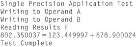
Figure 3.15 Output for Single Precision test running on the Xilinx ML510 development board.
3.B Embedded GNU/Linux System
Perhaps the greatest barrier to using free and open software in embedded systems is the learning curve. Over the next few chapters this text will introduce the bare minimum required to get started, including the tools and steps required to create a GNU/Linux-based system on a Platform FPGA. This section starts with the basic organization of a GNU/Linux filesystem, explains configuration and build tools, describes how to create a cross-compiler, builds a root filesystem, cross-compiles an application, and creates a cross-compiled kernel. That is a lot for one section but, fortunately, there are many supplemental resources available on the World Wide Web.
Specifically, we start with the organization of the UNIX filesystem, describe the two main configuration tools in use, and then how to build a cross-development environment. We then use these tools we just built to cross-compile Linux, build a root filesystem, and add a “Hello World!” application.
3.B.1 Organization of Unix Filesystem
If we are going to use a full-featured operating system, such as Linux, the first thing we have to concern ourselves with is the organization of the root filesystem. We need to decide where the required configuration files, system binaries (such as init), shared libraries, and application binaries will be located. We could put everything in the root directory, but as the number of files and supporting software packages increase, this becomes unwieldy. Likewise, we could come up with a completely novel scheme of directories and subdirectories — but again, this approach usually offers few advantages while potentially introducing considerable confusion. Instead, it makes sense to learn the conventional places to put things. Over the years a common hierarchy of directories has evolved and the Filesystem Hierarchy Standard (FHS) documents these de facto conventions. Using the convention minimizes the amount of configuration choices and reduces the chance of making a mistake. It is also much easier to ask for help from a colleague or the Internet if everything is where it normally is!
The first convention to follow is how to layout the directories and subdirectories of the root filesystem. (A detailed description of the entire tree for Linux can be found at www.pathname.com/fhs/.) A subset required for a medium-sized embedded system is described here. At the root, there are typically 15 directories. The directories bin, sbin, lib, and dev are used to hold general-purpose binaries, system binaries, shared/static library files, and device files, respectively. (Device files are used to provide applications with access to peripherals — we’ll revisit them in the next chapter.) The etc directory is used to store configuration files that generally don’t change frequently; the var directory is used to store run-time generated files that applications use to store state information or record events (such as log files). The directory boot is used by the bootloader to store configuration information about the different ways a system can be booted; embedded systems typically only use this directory during development since, in the field, the system only boots in one configuration. The home (or sometimes called users) directory has the home directories of all users except the super-user, root. The user root’s home directory is just root. The sys and proc are special directories used for accessing kernel information, which are discussed later. The directories opt and mnt are for convenience — some developers install “optional” software in the former and the latter is a convenient place to mount new, temporary filesystems. The directory tmp should be obvious.
The remaining directory typically found in the root is called usr. Pronounced user, this directory has several subdirectories that may seem redundant: bin, sbin, and lib. Why two binary directories (/bin and /usr/bin)? There are two practical reasons. In the past, larger systems periodically checked a filesystem for inconsistencies but because one can’t do a thorough check on a mounted filesystem, the system was booted without usr and a filesystem check could be performed. After the check, the root filesystem was extended by mounting the usr directory. Thus /bin and /sbin have the bare minimum to boot a system. The /usr/bin and other directories in /usr contain everything else needed to run the system.
Fortunately, one doesn’t have to memorize these things. In practice, there are a number of simple shell scripts that create a template root filesystem (the book’s Web site has one and its usage is explained shortly). Also, many Open Source packages already know the standard and automatically configure themselves to install in the proper locations. A typical layout is shown in Figure 3.16.
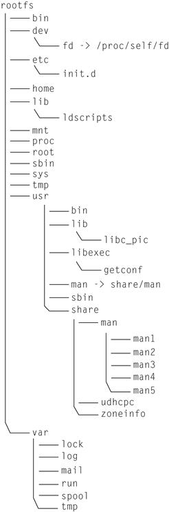
Figure 3.16 Typical bare-bones layout of FHS root filesystem.
3.B.2 Configuration Software and Tools
There are two popular configuration tools used with Open Source software today. The first is often referred to as the “autotools” or “configure script” approach. The former name refers to a set of tools (autoconf, automake, and libtool) used to create a set of Makefiles and a configure script. The latter name refers to the output of running the tools. In either case, these software tools are used by package developers to make their software portable and easy to install. The second major configuration technology is called a “menuconfig” system. This software was introduced to replace a slow question-answer system that was originally used to configure the Linux kernel. Since then, it has been adopted by several other packages. In addition to these configuration tools, a handful of other software tools are useful for collecting and managing software packages.
GNU Release Process
Most GNU software and many (non-GNU) open source packages come with a configure script. This script, among other things, prepares the software to be compiled and installed. UNIX and UNIX-like systems have a long and interesting history. As a result, different libraries of subroutines have evolved over time. There have been “best practices” that have emerged, peaked, and are now rarely employed. This has led to great diversity in terms of what features and subroutines might be available. The autoconf part of autotools was intended to interrogate the local system and then provide system configuration information to the application. Although many of the portability issues of the past have been resolved, the tools continue to be extremely useful in cross-compiling and installing application files. (Èric Lèvènez has an interesting Web page that summarizes how 100+ different versions of UNIX have influenced each other, http://www.levenez.com/unix/.)
The general process of installing a GNU package is:
1. Acquire the software (nowadays, this means downloading from the Internet) and unpack the software (uncompress and untar).
2. Go into the subdirectory created by unpacking and type:
./configure
3. Assuming that there were no incompatibilities that could not be worked around, the next step is to build the software package:
make
4. An optional step is to type “make check” — this will run regression tests and does a quick sanity check before the software is installed on your system
5. Assuming the software has compiled correctly and passed the optional regression check, the last step is to install the software. This is accomplished with
make install
This will not just copy the executables into the proper locations but also creates configuration files and anything else required to run the application.
By default, most software packages will install in a directory called /usr/local. This directory mirrors the /usr directory (in the sense that there is a /usr/local/bin, /usr/local/lib, /usr/local/include, etc.) and indicates that this is locally installed software that didn’t ship with the workstation.
However, the location is very easy to change. Most configure scripts allow the user to specify a prefix that changes the install location. For example, the command:
configure – –prefix=/usr}
will set up the software so that after it has been compiled, binaries will be installed in /usr/bin. In addition to —prefix there is another set of several options that let you further customize the specific directories that various types of files are installed. Most GNU packages have the option of adding arguments to the command that direct how the application is to be compiled and how it should behave.
Later it will become necessary to build the root filesystem in a subdirectory of another filesystem. Simply changing the —prefix option will not always work because some applications use the prefix to compile absolute paths inside the application. So instead of saying something like
./configure – –prefix=/home/rsass/build/rootfs/usr
![]()
make install
one can use an environment variable, DESTDIR, to point at the subdirectory that will be the root filesystem in the embedded system. It is used on the make install command as shown below.
./configure –prefix=/usr
![]()
make DESTDIR=/home/rsass/build/rootfs install
Some of the most important of these configuration options (at least for embedded systems) are the options that direct how to cross-compile the application. These are - -host, - -build, and - -target. Often in embedded systems, the “host” is the workstation where development and debugging take place and the “target” is the embedded system that is being developed. However, in GNU terminology, the terms host and target are used differently. So, for the moment, completely forget about target and we will just talk about the host machine and the build machine.
In GNU terminology, host refers to the machine that will ultimately execute the application. The configure script will assume the host is the machine the script is being run on, but in our case, the host is the processor and C library on our embedded system. So the host refers to what kind of binary executables we want to produce. Because these binaries will likely be dynamically linked to a library, the version of the C library is important as well. To tell the configure script to assume a different host, you use the –host argument. In GNU terminology, build refers to the machine we are going to use to compile the application. (Obviously, there has to be a cross-compiler on the build machine that knows how to produce the host’s executables.) Often, the configure can guess the build machine by assuming it is the one that ran the configure script. So this is only strictly necessary when the person installing the software knows they are going to run “make” on another machine. To tell to configure that the package will be compiled on a machine, one uses the - -build argument. (We will return to the - -target option at the end of this discussion.)
These three configure options take a single argument called a machine triple. A machine triple is a string that uses hyphens to specify a machine’s vendor, CPU model, and operating system. For example, sparc-sun-solaris indicates that the machine was manufactured by Sun, Inc., that the instruction set of the processor is SPARC, and that the OS is Solaris. This is in contrast to sun-sparc-sunos, which is the same hardware except that it is running the SunOS version of UNIX instead of Solaris. And, like a lot of things, it complicated. For example, if part of the machine triple is implied or is generic (therefore not relevant to configuring), then it can be omitted. For example, sparc-solaris is a legal abbreviation because the vendor is implied. Further complicating the situation is that some parts of the triple need more detail. So, for example, we will be using the PowerPC in the Virtex 5 for many of the examples, but the PowerPC has many variants designed for different roles. The PowerPC 604 was intended for desktops and workstations, while the PowerPC 405 and PowerPC 440 are for embedded systems. To indicate the model, powerpc-405 or powerpc-440 could be used in the slot for the CPU (making the machine triple look like it has four components!). Similarly, many operating systems need to be clarified. For example, in common parlance, people refer to a popular open source operating system as “Linux.” However, it is important to the configure script to know more. What most people mean by “Linux” is referred to more properly as linux-gnu. That is, the operating system kernel is Linux but the C library and the rest of the operating system come from GNU. In contrast, mach-gnu and hurd-gnu refer to the same library and OS utilities but are different OS kernels. So the machine triple for one of the authors’ laptops is i686-pc-linux-gnu. The vendor has been omitted, the processor is i686-pc, and the operating system is linux-gnu. Likewise, the hard procesor core found on the Virtex 5 is powerpc-440-linux-gnu. The hard procesor core found on the Virtex 4 is powerpc-405-linux-gnu. Thus, to configure a software package to be compiled an Intel desktop for the embedded PowerPC in a Virtex 5, one might use the following command.
Thus, to configure a software package to be compiled an Intel desktop for the embedded PowerPC in a Virtex 5, one might use the following command
./configure –prefix=/usr –build=i686-pc-linux-gnu–host=powerpc-440-linux-gnu
Table 3.1
Various machine triples.
| Machine Triple | Type of Machine |
| i686-pc-linux-gnu | 32-bit Intel processor Linux Distribution |
| x86_64-unknown-linux-gnu | 64-bit Intel processor Linux Distribution |
| sparc-sun-solaris2.9 | SPARC processor on Sun Inc. hardware running solaris |
| mips-sgi-irix6 | MIPS processor on SGI Inc. hardware running Irix |
This will tell the software package that ultimately this system is going to be transferred to a PowerPC running GNU/Linux and that the cross-development tools to use have the prefix powerpc-440-linux-gnu-. For example, the name of the C compiler would be powerpc-440-linux-gnu-gcc.
What about - -target? Well some applications are designed to use object files either as an input (a linker/loader) or as an output (an assembler). This introduces a third machine possibility: the package can be configured to be compiled on one machine (the build machine), executed on another (the host machine), and manipulate the object files of a third machine (the target machine). So, one might compile an assembler where the build and host machine are i686-pc-linux-gnu but the target is powerpc-440-linux-gnu. This would be a cross-assembler — it is an executable runs on Intel x86 machine but it takes PowerPC mnemonics and produce PowerPC object files. Clear? If not, you can use this rule of thumb: if the package has nothing to do with manipulating a machine’s object files then the - -target option is unneeded.
Menuconfig
For software, such as Web server or an XML parser, the number of configure/install options is relatively small (less than 50). However, for other software that is highly configurable (such as Crosstool-NG) it is unwieldy to specify these on a command line. Moreover, it is difficult to keep track of a specific configuration. To handle this better, the Menuconfig system was developed. The most common version is a Curses-based application that presents the person installing the software with a menu of choices. In the case of the Linux kernel, every choice has three options: Yes, No, or Module (indicated by a [*], [ ], and [M], respectively). Yes means that the option should be compiled into the kernel. No means that the option should not be compiled and no support for incorporating the option at run-time should be included. The Module option indicates that the option should be compiled separately from the kernel and provisions made so that the option can be inserted and removed at run-time. Device drivers are often compiled as modules. There is no reason to have every device driver in the kernel when a system is booted because there are several hundred devices supported by Linux but any one system is only going to have a handful of devices installed. If a USB thumb drive is plugged in at run-time, the appropriate modules are inserted dynamically and the system can start using the device immediately.
These related options are grouped together into menus and then related menus are grouped to form submenus of the main menu in a hierarchy.
The program is accessed by unpacking the software and typing:
make menuconfig
If the system being configured is going to be cross-compiled, it is a good habit to specify the architecture and cross-compiler. (For some applications that use menuconfig, this doesn’t matter, but for others it does.) So, for example, to configure the Linux kernel for the Virtex 5’s hard processor, one would type
make ARCH=powerpc CROSS_COMPILE=powerpc-440-linux-gnu- menuconfig
The ARCH environment variable tells menuconfig to ask questions specific to building PowerPC kernels. The CROSS_COMPILE environment variable tells menuconfig the prefix of cross-development tools. Note the trailing hyphen after the machine triple; this string is the prefix of cross-development tools so the hyphen is required. In other words, this is a prefix of a command, not a machine triple.
The input to menuconfig is one or more Kconfig files that have all of the configuration options to present to the person compiling the software. The output is a .config file. Both are plain ASCII files that are human-readable. The .config file has one option per line in the form of:
CT_GMP_MPFR=y
or
CT_GMP_MPFR=m
or
# CT_GMP_MPFR is not set
for “compile into the kernel,” “compile as a module,” and “don’t compile,” respectively.
This means that one can save a configuration by simply copying the .config file to another place (or name). It also means that one can quickly determine the differences between two configurations with the utilities such as diff. The Linux kernel has several architecture-specific default configurations included. The command
make ARCH=powerpc CROSS_COMPILE=powerpc-440-linux-gnu-44x/virtex5_defconfig
will create a default .config that is a reasonable starting point for the Xilinx ML-510 boards.
Note that if you create a .config manually (by copying it from somewhere, for example), you still need to run through the menuconfig system at least once or by typing
make ARCH=powerpc CROSS_COMPILE=powerpc-440-linux-gnu- oldconfig
3.B.3 Cross-Development Tools and Libraries
The traditional Board Support Package found in microcontroller-based embedded systems is relatively unchanging and works well for other embedded system platforms because it can rely on a number of fixed characteristics. Either the processor has a floating point unit or it doesn’t. Either there is RAM at a particular place in the address map or not. When there is variability in a traditional microcontroller-based system, it is fairly limited. Not so for Platform FPGAs! Although the hard processor core on the Virtex 5 FX device is fixed (a PowerPC 440) it is not the only processor option. In addition to the MicroBlaze that comes with XPS, there are a range of soft processor cores as SPARC and MIPS implementations. Furthermore, even the hard processor cores found on FPGAs can be customized. Thus, in addition to building hardware and creating the embedded system application, a Platform FPGA designer often has to build the cross-development tools and system software as well. Here we describe the steps used to build a GNU Compiler Collection (GCC) tool chain for the PowerPC 440 found on the Virtex 5 FX device. We assume that an FPU is not present. Only two changes are needed to build the tool chain for the Virtex 4’s PowerPC 405.
There are four (or five if you want a debugger) major software packages central to building a cross-development environment. The first is called the binutils package. The binutils package includes a number of primitive utilities to create and manipulate binaries. This includes an assembler, a linker/loader, and a collection of utilities that operate on object files. The next package is the C library, which provides a collection of standard subroutines for C (and other languages). The C compiler needs to have a C library available when it is compiled, this presents an interesting chicken-and-egg problem. Because most of the C library is written in C, it needs a cross-compiler to compile it. The solution is a multistage build where a minimal C compiler is created to cross-compile the library, which is then used to compile the full C (and other languages) cross-compiler(s). It is also worth noting that several C library options are available. The newlib C library is the simplest and often used in embedded systems without an operating system. There is the GNU C Library (GLIBC), which is a full-featured library. Recently, there is a fork of the GLIBC project called Embedded GNU C Library (EGLIBC), which is the one we’ll use here. The fourth essential software package is the Linux kernel. We are not going to cross-compile the Linux kernel at this point, but the compiler and the C library need to know what system calls are available, as well as the value of certain constants in the kernel’s header files. These interfaces are illustrated in Figure 3.17, and the interdependencies among the last three components are shown in Figure 3.18. What is needed are kernel headers, which can be extracted without building the entire kernel yet.
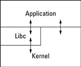
Figure 3.17 Interface relations.
Figure 3.18 Dependencies between tools.
So the high-level view of the process is as follows. Get the kernel headers, build the binutils for the PowerPC 440, build a static, minimal cross compiler, get Embedded GLIBC headers, recompile GCC, rebuild the full C library, and then build the full C compiler (and other languages) using the the “full” C library. Then we use our newly built cross-compiler to finish building binaries for the embedded system. Note that GCC 4.3 now requires two additional libraries: GMP and MPFR, which are libraries that implement arbitrary precision data types and multiprecision floating-point operations, respectively.
Downloading and Installing Crosstool-NG
This process is long, laborious, and error-prone. A wonderful script called crosstool.sh created by Dan Kegel (see http://www.kegel.com/crosstool/) has automated this procedure for a variety of processors and software versions. For years, it served the authors of this text well. However, as of this writing the latest vesion is 0.43 and that version is very out of date. GCC and GLIBC have evolved substantially since version is 0.43 of crosstool was released. Moreover, GCC’s adoption of GMP and MPFR means that the script cannot compile the latest versions.
Inspired by Kegel’s work, Yann Morin developed his own script to accomplish the same thing, automate the building of a cross-development tool chain. Kegel used a collection of data files with environment variables to manage the different processors and versions. Yann added a menuconfig-like interface. His system, called crosstool-NG, is invoked with the command
{% ct-ng}
and can be found at http://ymorin.is-a-geek.org/projects/crosstool. An interesting, but perfectly appropriate approach employed by Yann is to use a ./configure script to check that the host system has the required versions of the system tools needed to configure and compile the tool chains. This project is very active at the time of publication and it is the tool we currently use. We specifically recommend the following setup. Starting with the /opt directory that we used to install the Xilinx tools in Chapter 1, we install the ct-ng command and software tools needed compile the GCC tool chains in the directory /opt/crosstool-ng. Next we use crosstool-NG to build different versions of the tool chain. For example, we might have one version that uses a software library to emulate the PowerPC’s floating point operations and another version that assumes an floating-point unit has been synthesized. The directories might look as follows.
{/opt/crosstool-ng/powerpc-440-linux-gnu}
{/opt/crosstool-ng/powerpc-440-fpu-linux-gnu}
(Those directories contain the cross-compilers and cross-compiled libraries created by crosstool-ng.) Finally, we add a script /opt/crosstool-ng/bin to help create FHS compliant root filesystems and a settings.sh that, when sourced, will setup the user’s PATH and MANPATH environment variables.
The first step is to download, configure, and install crosstool-ng. This may require downloading the latest version of some of the autotools because a few well-known Linux distributions have not yet upgraded to the required version. (If crosstool-NG passes the configure stage, then you can skip the steps related to autoconf, automake, and lzma given later.) We also install genext2fs at this time — it will be needed when we build a root filesystem image in section 3.B.5. This package can be found at http://sourceforge.net/projects/genext2fs/files/. The detailed step-by-step proceedure is given on the books Web page. The last step is to add two scripts that can be found on the book’s Web site. The settings.sh script that we use also incorporates the path of a default cross-compiler and is illustrated in in Figure 3.19. The mkfhs.sh script creates a FHS compliant directory and populates it with some simple configuration files. This script can be copied into /opt/crosstool-ng/bin as well.
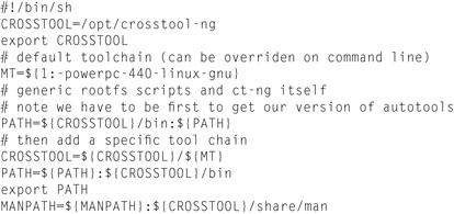
Figure 3.19 The settings.sh to set up environment.
This is a one-time process and the tools installed thus far will let us create multiple tool chains and will support multiple projects. To build a simple PowerPC 440 cross-compiler suitable for the hard processor core on the ML-510’s Virtex 5 chip, one would create a working directory and then run the ct-ng command. We will start with a PowerPC 405 configuration and then modify it for the 440. The general steps are
1. Create a default configuration with the command
ct-ng powerpc-405-linux-gnu
2. Edit the configuration with menuconfig
ct-ng menuconfig
and then under the “Paths and misc options” menu change the prefix to be /opt/crosstool-ng/ ${CT_TARGET}. Also change “Emit assembly” and “Tune” options under “Target options” menu from 405 to 440. Change the “Tuple’s vendor string” to 440 on the “Toolchain options” menu. And then, last, change the “C Library” from GLIBC to EGLIBC.
3. The last step is to build the cross-compiler tool chain with the commmand
ct-ng build
On an older desktop with a DSL modem, the process took 325 minutes to download and compile everything! A reasonably fast machine, with all of the software already downloaded, takes around 120 minutes. Detailed instructions with screenshots are on the book’s Web site.
Now that we have a cross-development tool chain, we are ready to write an application. To do this, we need to cross-compile an operating system, create a root filesystem, and cross-compile the application. We describe these remaining steps next.
Cross-Compiling Linux
If you know how to compile a Linux kernel, cross-compiling Linux is simple. However, compiling the Linux kernel can be intimidating to people that are new at it because there are an enormous number of options and many of the choices assume a significant knowledge of commodity desktop hardware and its history. While many of the hardware cores described earlier (such as the 16550 UART) have Linux device drivers that support it directly, there are others that do not. Obviously, any custom hardware cores that you develop for a project won’t have a Linux device driver for it!
The easiest way to get started and manage this complexity is to (1) rely on a Xilinx-maintained Linux repository that has Xilinx device drivers added to the kernel and (2) start with a known-to-work configuration and modify it. Fortunately, the 2.6 kernel series has a number of “default config” options that we can use.
3.B.4 Preparation
Before compiling Linux for the first time, there are a few things we need to do. The most important is to determine how to make Linux aware of our hardware design — including what hardware cores are included, how they are configured, and where they are located in the memory map. Also, as we begin to add more components to our Linux-based FPGA hardware, we describe some ways to organize these components.
In older versions of XPS and the Linux kernel, the common way of making device (hardware core) information from XPS available to the Linux kernel was by passing around an xparameters.h file. This file was generated by XPS as part of a Software Platform Settings option. By copying this file into the appropriate place in the Linux kernel’s source, the critical information could be determined at compile-time. This information is only relevant for existing projects that use the “ppc” architecture in the Linux kernel.
In 2009, maintainers of the “ppc” architecture (which was mostly used for embedded systems) switched to using the architecture “powerpc.” With this change, the way of communicating information about the hardware design in XPS to Linux changed as well. Instead of having an xparameters.h file at compile time, Linux uses a device tree file at boot. This approach allows the same compiled kernel to be used with multiple hardware designs — the designer simply configures the bootloader to pass a device tree to the kernel at boot. Alternatively, one can combine device tree information with the kernel at compile-time if one doesn’t have a bootloader that supports device tree files.
With version 11.4 of the XPS, it is necessary to add device tree support to XPS. Linux (and closely related tools) uses a source code management system called ’git.’ We won’t go into the details of git but the commands are relatively simple.
After installing XPS, one needs to download the device tree generator from Xilinx following the instructions listed on the book’s Web page.
Before downloading Linux, it is worthwhile to think a little bit about how to organize the growing number of components in a project. One way is illustrated in Figure 3.20. We create the hardware first in an hw directory, next we cross-compile Linux in a directory created by the git command, in the next section we’ll create the software that goes on the root filesystem, and then we finally combine the hardware and software together into an ACE file.
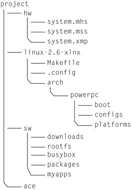
Figure 3.20 Typical directory structure of a project.
Building the Hardware Base System
We can quickly generate a hardware base system with the Base System Builder wizard from within XPS. Unlike the base systems generated previously, we must include a few additional components to support Linux. We will continue to use the Xilinx ML510 with the Virtex 5 FX130T FPGA. Create the base system described in Table 3.2.
Table 3.2
Base System Builder wizard options for a Linux base system.
| BSB Wizard Page | BSB Settings |
| Board Selection | Xilinx Virtex 5 ML510 Evaluation Platform Revision C |
| System Configuration | Single-Processor System |
| Processor Configuration | 400 MHz PowerPC processor with 100 MHz Bus |
| Peripherals | refer to Figure 3.21 |
In this base system we are preparing to support a Linux system running out of 512 MB of DDR2 memory, with Ethernet support, an RS232 UART interface running at 9600 baud, and and optional LCD display. We include 64 KB of BRAM for testing purposes. It is not necessary for future designs to include this much memory, although it is necessary to include some BRAM to boot up the initial system. The IIC EEPROM will be used in a future design in section 3.A.
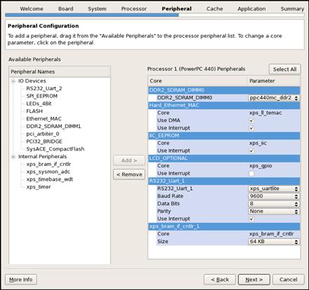
Figure 3.21 Peripherals needed for the “hello world” Linux system on the Xilinx ML510 development board.
Next we must Export Hardware Design to SDK, which will synthesize and generate the system’s bitstream along with creating the SDK project and launching the SDK.
From within the SDK we must generate a new Board Support Package project. We can name this project linux_bsp. Set the Board Support Package Type to device-tree. If this option is not available, be sure to download and install the device tree generator as instructed in Section 3.B.4.
Under the Board Support Package Settings window, change the field “bootargs” for the console from
console=ttyS0 root=/dev/ram
to
console=ttyUL0 root=/dev/ram
which specifies that we will be using the UART lite.
Now a xilinx.dts file should exist in your SDK Project’s directory under the following path:
% SDK/SDK_Workspace/linux_bsp/ppc440_0/libsrc/device-tree_v0_00_x
Remember this location as we will return to this file shortly when compiling Linux.
Compiling the Kernel
To get the most recent update of the Xilinx-maintained kernel from the Xilinx GIT repository. Detailed directions are available online as well from the book’s Web site.
Once the Linux kernel has been downloaded, we must configure it with a default Virtex 5 configuration. This is done to save us time navigating though the various menuconfig options. Change directories into the linux-2.6-xlnx directory and run the following make command
% cd linux-2.6-xlnx
% make ARCH=powerpc 44x/virtext5_defconfig
This copies the arch/powerpc/virtex5_defconfig configuration file in place of the .config file. Next we must copy our xilinx.dts file from our SDK directory to the DTS directory within the arch/powerpc/boot/dts directory. The DTS file specifies the components, their physical addresses, and other information pertaining to our hardware base system. When compiling Linux, the DTS file will provide the necessary information such that the system will be capable to correctly interface with our hardware.
With the DTS file in place and the default Linux configuration set for our PowerPC 440-based system, we can run menuconfig to set the “Default RAM Disk Size” to 16384. (This is found under the Block Device submenu under the Device Drivers menu.)
Now all that is left is to compile the Linux kernel.
% make ARCH=powerpc CROSS_COMPILE=powerpc-440-linux-gnu- simpleImage.xilinx
At this point we have a compiled Linux kernel that is configured to run with our specific hardware base system. Of course, a system with just a Linux kernel does not provide us with much. In fact, we will need to build the root filesystem before we will be able to boot the kernel on the Xilinx ML510 development board.
3.B.5 Building a Root Filesystem
Once we have the hardware, a cross-development tool chain, and a compiled kernel, the next step is to build a root filesystem. There are several reasonable options. If our FPGA board has a (removable) secondary storage device and the kernel has been configured for its interface, then we can use a partition on that filesystem to be our root filesystem. For example, many Xilinx FPGA boards have a CompactFlash drive that the SysACE (which programs the FPGA at power on) device uses to read stored bitstreams. Because the SysACE device only looks at the first partition, a Linux system can use another partition on the drive as a root filesystem. A second option is to use NFS — a Network File System protocol that allows a Linux system to mount a filesystem over a network (such as Ethernet). Of course, both of these options require that the proper kernel modules be compiled into the kernel. The NFS approach also requires that a DHCP and NFS servers be set up. Probably the easiest solution is to begin with is to build a RAMDISK image and include it with the kernel. Once this is mastered, switching to NFS for development work is generally faster. Having the root filesystem in flash makes the most sense when shipping the product.
One tells the Linux kernel where the root filesystem is by passing a command line argument to it. Table 3.3 shows the three options.
Table 3.3
Command line arguments to specify the location of the root file system.
| Location | Kernel Parameters (examples) |
| RAMDISK | root=/dev/ram |
| NFS | root=/dev/nfs nfsroot=192.168.1.101:/export/rootfs/n01 ip=dhcp |
| CompactFlash | root=/dev/xsa1 |
So a RAMDISK-based Linux system with the console on a UART Lite device (with a baud rate 115,200) would have the Linux command line
console=ttyUL0,115200 root=/dev/root
set during the kernel configuration, as we have already done.
Once we have a kernel, the next step is to create the root filesystem.
There are five basic steps to creating a root filesystem. The script we previously installed, mkfhs.sh (for “make filesystem hierarchy standard”), does three of them. You have to do one manually. Then genext2fs does the last step.
Specifically, the first thing is to create the sw directory in your project directory. In that directory run the script mkfhs. (If you sourced the settings.sh file in /opt/crosstool-ng, then this script will bin your path and the environment setup.)
The script is too long to include verbatim here but is available on the Web site. After checking to see that you don’t already have a rootfs created and that environment is correct, the first thing that it does is populate a directory, rootfs, with every dynamically linked library (shared object) that is used by the cross-development tools. Then it goes through and removes all of general computing system libraries and files to save space on our embedded systems root filesystem. Then it strips the debugging information from the shared objects — we assume that no one will want to debug the C library on an embedded system! The last thing it does is unpack a bunch of typical configuration files – the bare minimum required to boot a system.
Next we need to add system binaries to our root filesystem. That is, add the usual Linux command line applications such as /bin/ls and the command line shell. It is possible to build the entire root filesystem from scratch; in fact, there are many suitable Web sites to explain all of the details. One in particular that we find very useful is http://www.linuxfromscratch.org.
Alternatively, we quickly generate a root filesystem with the help of another package. BusyBox can be used to generate a majority of the binaries needed to boot and operate a Linux-based system on an FPGA, http://www.busybox.net. In you decide to use BusyBox (which is recommended for those relatively new to filesystems) we have detailed instructions on the book’s Web site on how to download, configure, and cross-compile Busybox.
In addition to the system binaries, this is when you add any kernel modules you have developed and your embedded application to the root filesystem. For this demonstration, we can just use the familiar “Hello, World!” program. If the program is in a file named hello_world.c, then we can cross-compile the application with powerpc-440-linux-gnu-gcc.
% powerpc-440-linux-gnu-gcc -o hello_world_440 hello_world.c
Even though the build machine cross-compiled the application, it will not be able to execute the newly cross-compiled application hello_world_440.
% ./hello_world_440
-bash: ./hello_world_440: cannot execute binary file
Instead, the executable must be copied into the root filesystem generated earlier. For convenience, copy the executable to the rootfs/root directory.
The last step is to create a filesystem image. This converts the subdirectory rootfs into a single file that is block-for-block identical to what would be found on the partition of a disk drive. One popular way of accomplishing this is to create an empty file and use the mount command with the loop back option. However, this requires root privileges and small mistakes as root can have catastrophic effects. A safer approach is to use the genext2fs command we installed earlier. Genext2fs was written by Xavier Bestel and allows a nonroot user to create an ext2 filesystem image from a directory and a device file. (The device file also allows the nonroot user the ability to change the owner of a file, set permissions, etc.)
After the root filesystem image is created, it is copied to the arch/powerpc/boot directory in Linux kernel. With the filesystem image in place, we can now combine Linux kernel previously created with our root filesystem using the command
% make ARCH=powerpc CROSS_COMPILE=powerpc-440-linux-gnu- simpleImage.initrd.xilinx
Note that “initrd” stands for “initial ramdisk.” Ramdisk is another term for the filesystem image and some general purpose Linux distributions use an initial ramdisk to load required kernel modules before accessing the disk drives.
The command generates the file simpleImage.initrd.xilinx.elf in the arch/powerpc/boot directory. At this point, we have all of the software for our embedded system in a single file. The last step is to combine this ELF file with the hardware’s download.bit bitstream file. This is accomplished with the xmd command and the genace.tcl script. One follows the same proceedure that was previously described in section 1.B.
3.B.6 Booting Linux on the ML510
Finally, we can copy the ACE file to the CompactFlash for our development board and boot the system. Linux will begin to boot with its output being displayed through the UART to a terminal program, such as minicom, as seen in Figure 3.22. The boot process should take less than a minute, depending on the configuration options selected. Once booted, the user can login with the default root login (which does not require a password).
Figure 3.22 Booting Linux on the Xilinx ML510.
Once logged in, the user can explore the Linux filesystem hierarchy and test the “Hello, World!” program that we added to our filesystem. Return to the /root subdirectory and the ls should show the hello_world_440 executable in the /root directory. You can test it with this command.
% ./hello_world_440
Hello World!
At this point, we have all of the rudimentary skills to develop application-specific Board Support Packages complete with cross-development tools and custom root filesystems. Next we can begin to look at more sophisticated applications and begin to develop simple kernel modules to interact with our hardware.
Exercises
P3.1. Which of the following is more abstract?
• a 2MUX with a, b, and a select line
P3.2. Name specific examples that will make a design less cohesive.
P3.3. Decoupling may lead to duplicate hardware. From a system perspective, why is this a positive characteristic?
P3.4. If reusing software means that the developer doesn’t have to write it, why do we say the reuse has a cost associated with it? Who pays that cost?
P3.5. What is the difference between an instance and an implementation? How is each denoted in UML?
P3.6. Consider a large combinational circuit that consists of five XORs, five ANDs, and five inverters. A proposed design divides this circuit into three modules: one module has all of the XORs gates, another has the AND gates, and a third has the inverters. Comment on the quality of this design.
P3.7. Suppose we have been asked to design a portable MP3 player. Draw a Use-Case diagram to identify the major functionalities of the system.
P3.8. How does a stand-alone C program that outputs “Hello, World!” differ from one running on a Linux-based system? Be sure to consider the compiler, the resulting executable, the operating mode of the processor, and run-time support provided.
P3.9. Does one need to create a root filesystem for a standalone C program? Is it required for a Linux-based system?
P3.10. How does a cross-compiler differ from a native compiler? Does one need both? Will a developer ever need more than one cross-compiler?
P3.11. Does the choice of the C library impact the choice of the operating system kernel? Does the C library impact the choice of a cross-compiler?
P3.12. What is the difference between a monitor and a bootloader? What does a monitor provide that is not found in a bootloader? What does a bootloader provide that is not found in a monitor?
P3.13. What is the address map? What makes the address map more dynamic in Platform FPGA design compared to a traditional microcontroller?
P3.14. What are the three components of a GNU machine triple? When can the triple appear with less than three components? Why do some appear to have more than three components?
P3.15. What are the typical steps involved in installing a standard GNU software package on a root filesystem?
P3.16. What is the difference between the directories /bin and /usr/bin?
P3.17. What is the output of the genext2fs command?
P3.18. What are the major differences between menuconfig. configure techniques for configuring software? Contrast what is done automatically for the developer and the number of options.
P3.19. Name three ways to mount a root filesystem. What are the advantages of each?
References
1. 1394 Trade Association. 1394 TA specifications 2010 January; Also available at http://www.1394ta.org/developers/Specifications.html; 2010 January; last accessed June 01, 2010.
2. Alhir SSi. UML in a nutshell Sebastopol, CA, USA: O’Reilly & Associates, Inc. 1998.
3. David W. OpenSPARC Internals Santa Clara, CA: Sun Microsytems, Inc; 2008.
4. Denk W. Das U-boot manual 2007; http://www.denx.de/wikiU-Boot; 2007; last accessed May 2010.
5. eCos. RedBoot user’s guide 2004; http://www.gnu.org/software/grub/; 2004; last accessed May 2010.
6. Electronics Industries Association. EIA standard RS-232-C Interface between data terminal equipment and data communication equipment employing serial data interchange Greenlawn, NY 1969.
7. Futral WT. InfiniBand architecture: development and deployment — A strategic guide to server I/O solutions Hillsboro, OR: Intel Press; 2001.
8. GNU Project. GRand unified bootloader 2007; http://www.gnu.org/software/grub/; 2007; last accessed May 2010.
9. Grimsrud K, Smith H. Serial ATA storage architecture and applications: Designing high-performance, cost-effective I/O solutions Hillsboro, OR: Intel Press; 2003.
10. Hennessy JL, Patterson DA. Computer architecture: A quantitative approach San Francisco, California: Morgan Kaufmann Publishers, Inc. 2002.
11. Holden B, Anderson D, Trodden J, Daves M. HyperTransport 3.1 interconnect technology Colorado Springs, CO: Mindshare Press; 2008.
12. HyperTransport Consortium. Hypertransport specifications 2010; Also available at http://www.hypertransport.org/default.cfm?page=HyperTransportSpecifications; 2010; last accessed June 01, 2010.
13. IBM. IBM coreConnect 2009; Also available at http://www-03.ibm.com/chips/products/coreconnect/; 2009; last accessed June 01, 2010.
14. InterNational Committee for Information Technology Standards T13. AT attachment storage interface 2010 January; Also available at http://www.t13.org; 2010 January; last accessed June 01, 2010.
15. PCIIG. PCI express specifications 2010; Also available at http://www.pcisig.com/specifications/pciexpress/; 2010; last accessed June 01, 2010.
16. Poulin JS, Caruso JM, Hancock DR. The business case for software reuse. IBM System Journal. 1993;32(4):567–594.
17. USB Implementers Forum (USB-IF). USB 2.0 specification 2010a; Also available at http://www.usb.org/developers/docs/; 2010a; last accessed June 01, 2010.
18. USB Implementers Forum (USB-IF). USB 3.0 specification 2010b; Also available at http://www.usb.org/developers/docs/; 2010b; last accessed June 01, 2010.
19. Wulf WA, McKee SA. Hitting the memory wall: Implications of the obvious. Computer Architecture News. 1995;23(1):20–24.
20. Xilinx, Inc. PLBV46 interface simplifications (SP026) v1.2 2008; last accessed June 01, 2010.
21. Xilinx, Inc. Embedded processor block in virtex-5 FPGAs (UG200) v1.7 2009a; last accessed June 01, 2010.
22. Xilinx, Inc. Floating-point operator generator data sheet (DS335) v5.0 2009b; last accessed June 01, 2010.
23. Xilinx, Inc. MicroBlaze processor reference guide (UG081) v10.3 2009c; last accessed June 01, 2010.
24. Xilinx, Inc. Processor local bus (PLB) v4.6 data sheet (DS531) v1.04a 2009d; last accessed June 01, 2010.
25. Xilinx, Inc. PicoBlaze 8-bit embedded microcontroller user guide (UG129) v2.0 2010; last accessed June 01, 2010.
1JTAG is an acronym for Joint Test Action Group. However, its use here and in practice is so different from its intended purpose that we just refer to it as JTAG.