
Managing Bandwidth
Computation Is Cheap, Bandwidth Is Everything
RCS Lab Mantra
Perhaps the most fundamental issue in building an FPGA computing system is managing the flow of data through the system. The computational resources in Platform FPGAs are enormous and, as we have seen in the previous chapter, specific algorithms often have plentiful parallelism, especially if there is a computation that is specialized and relatively small. In this case it is very easy to instantiate a large number of those function units on a single chip. However, without considering the rates at which various function units consume and produce data, it is very likely that any potential performance gains may be lost because the function units are idle, waiting to receive their inputs or transmit their results. Performance issues include both rate of computation and power because an idle function unit is still using static power. There is also a correctness issue for some real-time systems as well. It is often the case that data are arriving from an instrument at a fixed rate — failing to process data in time is frequently considered a fault.
In this chapter the learning objects are related to examining bandwidth issues in a custom computing system.
• Starting out, Section 6.1 looks at the problem of balancing bandwidth, that is, to maximize throughput in a spatial design with the minimum amount of resources.
• Then, considering the target is a Platform FPGA, we spend time discussing the various methods used to access memory, both on-chip and off-chip, along with managing bandwidth when dealing with streaming data from instruments off-chip.
• Finally, we close this chapter with a discussion of portability and scaling with respect to a system’s performance in Section 6.3. As semiconductor technology advances, system designers are provided more configurable resources to take advantage of. The issue now is not one of “how do I add more function units?” but rather “how do I scale the bandwidth of the interconnection network?”
6.1 Balancing Bandwidth
Let’s begin with a motivating example. Suppose we have a simple computation, ![]() , that we need to apply repeatedly to a large number of sequential inputs. A simple spatial design of locally communicating function units is shown in Figure 6.1.
, that we need to apply repeatedly to a large number of sequential inputs. A simple spatial design of locally communicating function units is shown in Figure 6.1.
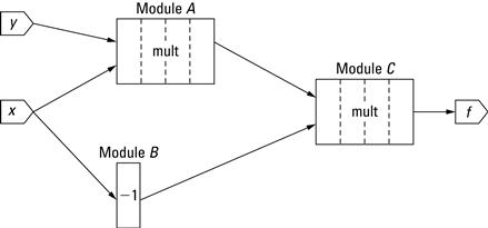
Figure 6.1 A simple network used to compute ![]() .
.
In order to maximize the frequency of the design, it is likely that the multipliers chosen for this design will be pipelined, and for this example it is assumed that these multipliers will have four levels of pipelining. We will also assume that the ![]() unit completes in a single-cycle operation.
unit completes in a single-cycle operation.
Now let’s analyze the timing in this example. At ![]() , the inputs
, the inputs ![]() and
and ![]() are present at the inputs of modules
are present at the inputs of modules ![]() and
and ![]() . At
. At ![]() ,
, ![]() has been computed and the result is present at the input of module
has been computed and the result is present at the input of module ![]() . However, the product
. However, the product ![]() is still being computed, so we have to stall the computation. A stall occurs in two cases: (1) whenever a computation unit has some, but not all, of its inputs or (2) when it does not have the ability to store its output, that is, the unit is prevented from proceeding because it is waiting on one or more inputs or waiting to store a result. Thus, module
is still being computed, so we have to stall the computation. A stall occurs in two cases: (1) whenever a computation unit has some, but not all, of its inputs or (2) when it does not have the ability to store its output, that is, the unit is prevented from proceeding because it is waiting on one or more inputs or waiting to store a result. Thus, module ![]() is stalled as well because it has to hold its result until module
is stalled as well because it has to hold its result until module ![]() uses it. These units continue to stall until
uses it. These units continue to stall until ![]() , at which point module
, at which point module ![]() produces its product, which then allows module
produces its product, which then allows module ![]() to consume both data and — for exactly one cycle — all three units can proceed in parallel. (Module
to consume both data and — for exactly one cycle — all three units can proceed in parallel. (Module ![]() is operating on the first two
is operating on the first two ![]() and
and ![]() values while modules
values while modules ![]() and
and ![]() begin operating on the next two
begin operating on the next two ![]() and
and ![]() values.)
values.)
Clearly, this pattern is going to repeat and modules ![]() and
and ![]() will stall again until
will stall again until ![]() . This is shown graphically in Figure 6.2. So if we have
. This is shown graphically in Figure 6.2. So if we have ![]() number of
number of ![]() and
and ![]() inputs, the network will take
inputs, the network will take ![]() cycles to compute all of the results. This is undesirable because one-quarter of our module cycles are spent waiting for data!1
cycles to compute all of the results. This is undesirable because one-quarter of our module cycles are spent waiting for data!1
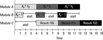
Figure 6.2 Illustration of the stalls example.
Even though FPGA resources have been allocated to these units, they are not contributing to the solution when they are idle. Moreover, they are continuously consuming static power — even if the transistors are not changing values. Finally, the throughput (one result every four cycles) is not much better than a time-multiplexed solution and probably slower than a general-purpose processor (which will have a faster clock frequency). What we aim for is a throughput of one result every cycle.
Readers may already recognize the solution to this problem. By adding a four-stage FIFO or buffer into the network, we can make this computation produce a new result every cycle after ![]() . There is more than one place to insert these buffers, but Figure 6.3 shows three buffers following the results of module
. There is more than one place to insert these buffers, but Figure 6.3 shows three buffers following the results of module ![]() . The introduction of buffers so that a network of computations does not stall is known as pipeline balancing. Chapter 5 discussed pipelining, both in terms of between compute cores and within individual computations. Implicit is the problem of how to best balance the pipeline. This problem is further complicated when dealing with larger systems that span multiple compute cores operating at different frequencies. Through the rest of this chapter we aim to address these problems with respect to Platform FPGA designs.
. The introduction of buffers so that a network of computations does not stall is known as pipeline balancing. Chapter 5 discussed pipelining, both in terms of between compute cores and within individual computations. Implicit is the problem of how to best balance the pipeline. This problem is further complicated when dealing with larger systems that span multiple compute cores operating at different frequencies. Through the rest of this chapter we aim to address these problems with respect to Platform FPGA designs.

Figure 6.3 High-throughput network to compute ![]() .
.
6.1.1 Kahn Process Network
In the previous stalls example, we built our network of computational components in a style known as a Kahn Process Network (KPN) Kahn (1974). In a KPN, one or more processes are communicating through FIFOs, with blocking reads and nonblocking writes. By this we mean it is assumed that the system is designed to support writing into a FIFO without the FIFO becoming full and losing data. Graphically, a KPN resembles a conventional streaming architecture where the source writes to the destination, as seen in Figure 6.4. Here, each node (circle) represents a process and each edge (![]() ,
, ![]() ,
, ![]() ) between the nodes is a unidirectional communication channel.
) between the nodes is a unidirectional communication channel.

Figure 6.4 Kahn process network diagram of a simple single precision floating-point system.
The network, which is represented as a directed graph, is also called a data-flow graph. As part of the example, we mentioned that the operation only begins when all of its inputs are available and there is a place for it to write its output. This requirement is called the data-flow firing rule. A short finite state machine, as seen in Figure 6.5, can be implemented to support the data-flow firing rule.
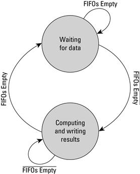
Figure 6.5 Wait/compute states of Kahn process network finite state machine.
We already implemented a Kahn process network in Section 3.A when we built the single precision floating-point adder. In that example, before processing data (performing the addition), we had to wait until not only both operands arrived into their FIFOs, but that result FIFO was ready to receive the added result and the adder was ready for new inputs as well. Had we not checked the status of result FIFO it would have been feasible for the system to have lost data between the inputs and the results by allowing the adder to consume data from the input FIFOs, but not being able to store the results.
An additional feature found in our single precision addition system is the ability to check the status of each FIFO, whether they were full or empty, in parallel to the FIFO read and write operations. This is in contrast to a conventional software implementation where the status of the FIFO would first need to be read prior to any operations occurring. As a result, in a software implementation, these sequential operations can add extra latency to the system. Through the explicit parallelism with FPGAs we can begin to see and understand the effects that something as simple as independent FIFO operations have on the efficiency of the system.
While the Kahn process network supports the unidirectional flow of data from a source to a final destination, it does not offer any mechanism to provide feedback between compute processes. The requirement of “unbound” FIFOs between processes makes for challenging designs in systems where FIFOs are a fixed resource that cannot be reallocated, that is, with FPGAs, when the Block RAM has been allocated as a FIFO and the design is synthesized and mapped to the device, that memory is fixed to that process. Instead, we will see that Platform FPGA designs can quickly incorporate the Kahn process network with fixed on-chip memory resources by including feedback between the compute cores. This approach is discussed within both Section 6.A and Chapter 7.
6.1.2 Synchronous Design
In a systolic data-flow implementation, every operation shares the same clock and data are injected into the network every clock cycle. If we can determine at design time that all data will arrive at the inputs at the right time (as was done in the second implementation of the network in the example), then we can avoid checking the data-flow firing rules and we get maximum throughput. Moreover, the FIFOs used in the example can be replaced with a smaller chain of buffers. This is called a synchronous design.
6.1.3 Asynchronous Design
In contrast, the asynchronous design strategy uses simple finite state machines to read inputs, drive the computation, and write the outputs. This requires additional resources, but has the bene-fit that there is no global clock, so the design can be partitioned across different clock domains. If the buffers are added as in the second implementation example, then it too has the benefit of getting maximum throughput.
In both synchronous and asynchronous cases, we have assumed that each operation takes a fixed number of clock cycles. However, the model can be extended to also include variable-length latency operations by using the maximum latency (to always get maximum throughput). The asynchronous design can use the most frequent latency to usually get maximum throughput.
The key to both of these design strategies is that FIFOs have the correct minimum depth. However, we do not want to waste resources — especially memory resources that are relatively scarce on an FPGA device. So the key to this problem is to find the mini-mum number of buffers needed to maximize throughput. The next section investigates how to best utilize the bandwidth of the FPGA in terms of on-chip communication, off-chip memory, and streaming instrument inputs.
6.2 Platform FPGA Bandwidth Techniques
As with the partitioning problem in Chapter 4, the analytical solution is most useful as a general guide to solving the problem rather than an automatic tool. Unfortunately, just as before, practical issues complicate the clean mathematical analysis. This section considers two places where these techniques can be applied and then considers some practical issues. First, we will look at integrating designs with on-chip and off-chip memory. A variety of memory types and interfaces exist and understanding when each is applicable is important to Platform FPGA designs.
Then, we will consider data streaming into the FPGA from some instrument. For practical embedded systems designs the “instrument” may be a sensor (such as temperature or accelerometer), some digitally converted signal (say from an antenna or radar), or even low-speed devices such as keyboards and mice. In some cases the instrument may need to use off-chip memory as a buffer or as intermediate storage, so while these two sections are presented individually, designs may require that the two functionalities be combined together. Clearly, we cannot discuss every type of instrument; for brevity we focus our attention on high-speed devices, which cause tighter constraints in FPGA designs.
6.2.1 On-Chip and Off-Chip Memory
Most embedded systems will require some amount of on-chip and/or off-chip memory (RAM) because many modern systems are data-intensive. This often means that the designer has to pay some attention to the memory subsystem. As mentioned earlier, the FPGA fabric does not include embedded caches found with modern processors.2 As a result, the designer must be aware of the system’s memory requirements in order to implement a suitable interface to memory so as to not create a memory bottleneck.
Memory requirements differ between software and hardware designs. In software there is less of an emphasis on where data are stored so long as they are quickly available to the processor when they are needed. When writing an application, the programmer does not typically specify in which type of memory (disk, Flash, RAM, registers) data should reside. Instead, more conventional memory hierarchy, depicted in Figure 6.6, is used. This is the typical hierarchy covered in computer organization textbooks. The ![]() axis refers to capacity and the
axis refers to capacity and the ![]() axis refers to access time. Non-volatile storage such as hard drives provide greater capacity, but at the cost of performance. Access times are typically in the millisecond range. Volatile storage such as off-chip memory provides less storage than disk, but typically at least an order of magnitude faster access times. Cache and registers occupy the peak, providing small but fast access. We mention this because unlike programmers targeting general-purpose processors, who are able to exploit caches and the system’s memory hierarchy, Platform FPGA designers must either construct custom caches or rely upon a modified memory hierarchy.
axis refers to access time. Non-volatile storage such as hard drives provide greater capacity, but at the cost of performance. Access times are typically in the millisecond range. Volatile storage such as off-chip memory provides less storage than disk, but typically at least an order of magnitude faster access times. Cache and registers occupy the peak, providing small but fast access. We mention this because unlike programmers targeting general-purpose processors, who are able to exploit caches and the system’s memory hierarchy, Platform FPGA designers must either construct custom caches or rely upon a modified memory hierarchy.

Figure 6.6 Traditional memory hierarchy comparing storage capacity to access times.
From a custom compute core’s perspective, we modify the drawing of the memory hierarchy for Platform FPGAs by removing the cache and replacing it with user-controlled local and remote on-chip memory (storage), as shown in Figure 6.7. On-chip memory is considered local storage when the memory resides within a custom compute core, maybe as Block RAM. Remote storage is still on-chip memory, except that it does not reside within the compute core. An example of this is on-chip memory that is connected to a bus, accessible to any core through a bus transaction. There is a fine line between local and remote storage. In fact, the locality is relative to the accessing core. If compute core A needed to read data from compute core B’s local memory, we would say that A’s remote memory is B’s local memory.

Figure 6.7 FPGA compute core’s memory hierarchy with local/remote storage in place of cache.
Figure 6.8 shows the various memory locations from a compute core’s perspective. Here, the register’s values are valid to the compute core immediately for read or write access. Local storage access is short, within a few clock cycles, whereas remote storage is longer, within a few tens of clock cycles. In the example the compute core would need to traverse the bus in order to retrieve remote storage data. Finally, we show the off-chip memory controller to provide access to off-chip memory. Access times to off-chip memory range in the tens to hundreds of clock cycles since the request travels off-chip.

Figure 6.8 Various memory locations with respect to an FPGA’s compute core with access times increasing from registers, to local storage, to remote storage, and finally to off-chip memory.
While physically there is a difference between cache and on-chip local/remote storage, the concept of moving frequently used data closer to the computation unit remains the same. The difference is the controlling mechanism. For caches, sophisticated controllers support various data replacement policies, such as direct-mapped, set associative, and least recently used. In Platform FPGA designs we are left to implement our own controller. This may seem like a lot of additional work, but keep in mind many custom compute cores most likely do not follow conventional memory access patterns or protocols, so creating custom controllers may actually be necessary to achieve higher computation rates.
Unlike most software programmers, hardware designers must be aware of the physical location of data to be processed. We must know whether data are in registers ready to be computed upon, in on-chip memory requiring reads through a standard interface such as a Block RAM, or in off-chip memory requiring additional logic (and time) to retrieve data. In each of these cases, the mechanism to access data may differ. Consider reading data from a regis-ter; data are always able to be accessed (and modified), typically within a single clock cycle. The designer references the register by name rather than by address. In contrast, consider how to access data from an on-chip memory, such as Block RAM. When using on-chip memories, we must include a set of handshaking signals. These signals may consist of address, data in, data out, read enable, and write enable. In this case, the memory is located within the compute core. This allows for fast access from the compute core, but can limit access by other compute cores. This is similar to a nonshared level 1 cache in terms of accessibility. Read and write access times are typically within one to two clock cycles.
The Block RAM can also be connected to the bus to provide more compute cores access to the memory. This comes at a cost of traversing the bus. The memory is still on-chip, but the interface to access the memory changes to a bus request. We mention this case because it more closely models one implementation for interfacing with off-chip memory, namely through a bus. However, for off-chip memory, instead of a simple bus interface to translate bus requests into Block RAM requests, additional logic is required to correctly signal the physical off-chip memory component.
Off-Chip Memory Controllers
The additional logic is in the form of a memory controller. In Platform FPGA designs, memory controllers reside on-chip as a soft core that interfaces between off-chip memory and the compute cores. The memory controller is responsible for turning memory requests into signals sent off-chip, freeing the designer from adding this signaling complexity into every compute core needing access to off-chip memory and, if multiple cores need off-chip access, having to multiplex between the requests ourselves.
Because the memory controller is a soft core, it is possible to construct different interfaces to both off-chip memory and on-chip compute cores. For example, in Figure 6.9, the memory controller is connected directly to the processor. Alternatively, the memory controller could be connected to a shared bus to allow other cores to access off-chip memory, as seen in Figure 6.10. Simi-larly, some memory controllers can provide direct access to more than one component; Figure 6.11 shows both the processor and the compute core interfacing to the memory controller directly.

Figure 6.9 The processor is connected directly to the memory controller.
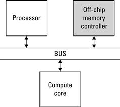
Figure 6.10 The memory controller is connected to a shared bus to support requests by any core on the bus.
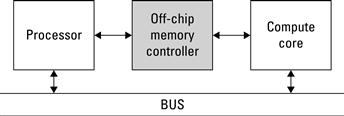
Figure 6.11 The processor and compute core are connected directly to the memory controller.
A conventional system may use a bus-based memory controller to provide the greatest flexibility in the design, allowing any master on the bus to read or write to off-chip memory. In Platform FPGA designs this type of access may suffice for many components, but providing a custom compute core with the ability to access memory directly can yield significant performance advantages that are otherwise unrealizable in traditional microprocessor designs. We discuss how memory accesses differ with these physical implementations shortly.
Memory Types
Up until now we have ignored the type of off-chip memory we have chosen to interface with. When purchasing development boards, vendors often populate the boards with one or more types of memory. These may include DDR SDRAM, DDR2 SDRAM, SRAM, Flash memory, EEPROM, etc. For those less familiar with these memories, you may be thinking of how they differ. For example, SDRAM versus SRAM differ in terms of latency, capacity, and maybe most noticeably cost (SRAM costs are significantly greater than SDRAM). SDRAM versus Flash memory differs in terms of long-term volatile versus nonvolatile storage and access time. With such a wide variety of memory, we must familiarize ourselves with the diff-erent memory controllers. This task may seem daunting, and for designers who are required to build a memory controller from scratch, it can be. However, in many cases, memory controllers have already been designed that can be instantiated from a repository/library of soft cores. This is one of the strongest benefits when designing with Platform FPGAs, using commodity off-the-shelf components (in our case hardware cores) whenever possible in a design.
When starting a design, it is common to begin with a development board that may contain various necessary and unnecessary peripherals. Vendors typically supplement these development boards with a repository of IP cores, which allows systems to be assembled rapidly. Within these repositories exist different memory controllers that can be instantiated within the design to provide access to the development board’s off-chip memory. Ultimately, a design will move away from the development board to a custom design, which may mean a different type (or capacity) of memory.
Fortunately, with some adjustments and modifications to the generics of the memory controller hardware core, different memory can be used [for example, using error correcting code (ECC) logic if the SDRAM DIMM supports it or not]. The goal of this section is not to teach you how to build a memory controller from scratch, but to understand how the different memory controller interfaces can affect a design. Specifically, we are interested in the memory access associated with these different interfaces. This is a shift from traditional processors where all of the computation is done by the processor, so one type of memory access may be all that is necessary. In Platform FPGA designs we can incorporate many different memory access types to support lower resource utilization, lower latency, or higher bandwidth memory requirements when needed. Moreover, we can provide some compute cores with high bandwidth access to memory while limiting memory access to other cores.
Memory Access
How the memory controllers are connected and used can have a dramatic effect on the system, even if a highly efficient memory controller and type of memory is used. It is up to the designer to understand how to connect the memory controller in order to meet the memory bandwidth needs. In Platform FPGA terms, the important trade-off is resource utilization.
Programmable I/O
For starters, the processor can handle transfers between memory and compute cores. With programmable I/O the processor performs requests on behalf of the compute core. This approach uses a limited amount of resources. The requirement is that each compute core be located on the same bus as the processor. The processor can read data from memory and write it to the compute core, or the processor can read data from the compute core and write it to memory. In this situation, the processor plays the central communication role. As a result, the processor may end up performing less computation while performing these memory transactions on behalf of the compute cores.
The effect is less noticeable as the amount of computation performed in the FPGA fabric increases, reducing the amount of computation being performed by the processor. In practice, there are a variety of ways to pass data among the processor, memory, and compute core. From the processor’s perspective, both memory and the compute core are slaves on the system bus with a fixed address range.
A software approach, such as C/C++, could involve pointers where the processor would access data stored in off-chip memory and then pass it to the compute core. We can also use pointers to provide array-indexed access to off-chip memory. Figure 6.9 depicts the system design used to connect the processor, memory, and compute core to allow data to be transferred from off-chip memory to a custom compute core.
Listing 6.1 provides a simple example of a stand-alone C application to read data from off-chip memory and transfer it to a compute core. We assume that the address space of the off-chip memory controller begins at address 0x10000000 and that the compute core begins at address 0x40000000. The functionality of the compute core is irrelevant for this example; just assume that writing data to its base address is how the processor interfaces with the compute core. Accessing memory as an array, mem_ptr[i], reduces the complexity associated with pointers. In this case, because both pointers were defined as type int (and we assume the processor is a 32-bit processor), incrementing the pointer results in reading from and writing to the next 32-bit data word.
DMA Controller
As a simple solution to the memory transfer problem, the processor doing the work may be acceptable; however, it is certainly not efficient. The time the processor spends reading and writing data is time that could be spent performing other computations. Most modern processors circumvent this problem by introducing Direct Memory Access (DMA) to perform memory transactions in place of the processor. There are variations on the implementation, but the basic idea is that the processor issues a request to the DMA controller, which then performs the memory transaction. This frees the processor to perform other computations while the DMA controller is operating. This works by allowing the DMA controller to act as both a bus slave and a bus master. As a slave, the DMA controller responds to requests from the processor (or any other bus master) to set up a memory transaction. Then, as a master, the DMA controller arbitrates for the bus and communicates with the memory controller to complete the memory transaction. The order of communication depends on the direction of the transfer (memory read versus memory write), so it is possible to issue a read from a compute core and write data to off-chip memory. To set up the transaction, the DMA controller needs at least the following information: source address, destination address, and transfer length. The source address is where data should be read from, the destination address is where data are to be written to, and the transfer length is the number of bytes in the transfer. Figure 6.12 is a block diagram representation of a simple system, including a processor, DMA controller, memory controller, and compute core.
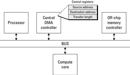
Figure 6.12 Central DMA controller to offload memory transactions from the processor.
Bus-Based DMA Interface
While the DMA controller may add an improvement in performance by reducing the overall involvement by the processor, there are still drawbacks. In the programmable I/O implementation the processor’s compute capacity is degraded when it performs the memory transactions on behalf of the compute core. Recalling the example (Listing 6.1) where during the for-loop the processor is acting as a middleman between memory and the compute core, we can free the processor from much of this responsibility by adding a DMA controller to perform the bulk of the work for each memory transaction. This approach is an improvement, but the processor is still involved and data must still be passed between the DMA controller and the compute core.
We can improve this further by giving each compute core the ability to issue transactions to memory independently. This is still considered DMA, but instead of a centralized DMA controller performing transactions, each compute core can independently issue its own read or write transactions to the memory controller. With a bus connecting the compute cores and memory controller, the arbiter for the bus becomes the communication controller, managing requests for bus access to issue memory transactions. The memory controller still only sees a single transaction at a time (note that some memory controllers can handle more than a single transaction at a time).
To support DMA within a custom compute core, additional logic must be added to the core’s interface. Typically, a core can be viewed as a bus slave, responding to requests from other cores on the bus. The example of programmable I/O where the processor writes data to the compute core is an example of this interface. A slave device cannot issue requests on the bus; in order to do so we must make the device a bus master. It is possible for a core to be a slave, a master, or both a slave and a master. Although, practically speaking, a core is usually only a bus slave or both a bus slave and a master. The processor is one of the few bus master-only cores.
That being said, for DMA support we only need a bus master, but we will include a bus slave to allow the processor and other compute cores to still communicate with the core. Because the bus interface depends on the actual bus used in the design, the specifics of the finite state machine needed to incorporate a bus master into a custom compute core will be covered in Section 6.A. From a hardware core’s perspective, a master transaction involves asserting the request to the bus arbiter, waiting for the arbiter to grant bus access, and waiting for the request to complete.
We mention bus master information because the memory controller is viewed as a slave on the bus. Once the memory controller responds to the bus transaction, the next core can issue its memory request across the bus. This approach alleviates the processor from performing memory transactions on behalf of compute cores and can improve performance by allowing a transaction to only traverse the bus once (previously, the processor would fetch data and then pass data to the compute core, requiring two trips across the bus). Requests to the memory controller are still performed sequentially by the bus, but any core that can be granted access to the bus can issue requests.
Direct Connect DMA Interface
In some situations it may not be necessary for every core to access off-chip memory. While we could create bus masters and bus slaves accordingly, a larger question should be addressed, namely, why not directly connect compute cores to the memory controller? This approach avoids contention for the bus, especially from other cores that need the bus but do not need access to the memory controller. Overall, this results in lower latency and higher bandwidth transactions to memory. A direct connect to the memory controller does require additional resources, both for the compute core and the memory controller. Some vendors supply memory controllers with multiple access ports (Xilinx offers a multiport memory controller, MPMC). Section 6.A presents one custom direct connect interface for the Xilinx MPMC known as the Native Port Interface.
By circumventing the bus, memory transactions no longer need to arbitrate for the bus, which reduces latency. In designs that require low latency, this may be the only way to meet the timing requirements. In some designs, only a few compute cores may need direct access to memory, and under these conditions is it feasible to directly connect the cores to the memory controller. As the number of cores needing access to memory increases, using a bus-based DMA interface is more appropriate, as each direct connect DMA interface requires resources that would normally be shared by a bus implementation.
One mechanism used to hide latency to off-chip memory is double buffering. Double buffering refers to requests that are made while the previous request is still in transit. This allows the memory controller to begin responding to the second request while the first request finishes. During read requests from memory, using double buffering can result in a best-case effective zero latency access for all requests after the first request.
Memory Bandwidth
When implementing designs we must be aware of the memory requirements before building the system. One important consideration mentioned earlier in this chapter is bandwidth. Bandwidth can be calculated based on the operating frequency and data width. For example, a bus operating at 100 MHz over 64-bit data words offers:
![]()
Calculating the bandwidth requirements of a compute core can help identify what type of memory controller and interconnect is suitable for the design.
In addition to raw bandwidth, we must consider setup times and latency. When a compute core initiates a transfer, depending on the interconnect, the request may need to wait to be granted access to master the bus, wait for the memory controller to complete its current transaction, or wait for data to be returned. To improve this latency would require a more directly connected interface to memory and/or operating the memory controller at a higher frequency, allowing it to perform more operations in the same time period.
Alternatively, a core may issue burst transfers. A burst transfer allows the compute core to issue a single request to the memory controller to read or write multiple sequential data, as depicted in Figure 6.13. This reduces the number of total memory transactions needed by allowing a single transaction to span more than a single data word and can save a significant amount of time when transferring large amounts of data. In a burst transfer the latency for the first datum is still the same, but each datum after the first arrives in a pipelined fashion, one datum per clock cycle. For example, a burst transfer of four 32-bit sequential data words would take the initial latency time for the first word, denoted as ![]() , plus three clock cycles for the remaining three words:
, plus three clock cycles for the remaining three words:
![]()
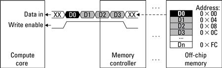
Figure 6.13 Burst transfer of four 32-bit sequential data words from off-chip memory to a compute core.
There are, unfortunately, two limitations to burst transfers. The first is data must be in a contiguous memory region. A burst transfer consists of a base address and a burst length. Data are transferred starting from the base address up to the burst length. The second is that the length may be limited by an upper bound, requiring multiple burst transactions for such large request lengths. As of this writing, Xilinx imposes a 16-word upper bound on memory requests across a bus and through a direct connect to off-chip memory.
To summarize, what we are trying to emphasize is that unlike traditional microprocessors, Platform FPGAs provide a flexibility to solve complex bandwidth needs. The flexibility sometimes comes at a price, often in terms of resources or programmability. Understanding when and how to chose the right combination is a responsibility the system designer must not take lightly.
6.2.2 Streaming Instrument Data
So far we have focused on interfacing with on/off-chip memory, but many embedded systems designers often face situations where the system must incorporate an application-specific instrument. An exotic example is a system with a number of science instruments flying on a satellite circling the Earth. These instruments are usually “dumb” in that they incorporate very little control and often have very little storage. Once turned on, they begin generating data at a fixed rate. It is up to the computing system to process this data and transmit it to the receiving station within a specific time frame (in this case, when the satellite is over the receiving station on earth). Unlike the off-chip memory problem where the consequence of a poor memory hierarchy is bad performance, the consequence of not being ready to accept data from an instrument is lost data. Data can be lost in two ways: if the device cannot process data arriving from the instruments fast enough or if the device cannot transmit the computed results back, to earth in this example, within the requisite amount of time.
There are plenty of less exotic examples as well. Embedded video cameras and other embedded systems sensors have similar characteristics. Data arrive at some fixed rate and must be processed, otherwise they may be lost. For commercial components, failure to do so results in loss of sales and unsatisfied customers.
These examples essentially break down to bandwidth issues: can the FPGA perform the necessary computation in the specified time period and, if not, how can we buffer data so as to not lose it? This is the focus of this section, how to support high bandwidth instruments. Chapter 7 explores a variety of interconnects that can be used to interface with external devices. In this chapter it is all about bandwidth, how to plan for it, and how to use it. We also are interested in using on-chip and off-chip memory intelligently for short-term storage when the need arises to buffer data.
Many instruments may have a fixed sample rate, say, every 10 milliseconds, and the device must operate on new data. The designer can calculate the exact amount of time allotted to processing data and work to design a compute core accordingly. As the sample rate increases, the amount of time to process data decreases unless the designer prepares the system to be pipelined as described in the previous chapter.
Traditionally, we have considered pipelines as a mechanism to achieve higher overall throughput in general-purpose computers. Here we use them not only to achieve high throughput, but to alleviate the tight timing constraints that may be placed on a designer with a high sampling rate. The requirement on pipelining is that the sampling rate (arrival rate of new data) be less than or equal to the slowest stage in the pipeline. Even still, this requirement can be circumvented if each stage is pipelined as well; however, at this point it becomes a granularity debate as to what is a stage in the pipeline. With the use of pipelines we can view the flow of data from the instrument through each compute core and finally to its destination as a stream. FPGAs can efficiently handle multiple streams in parallel at very high frequencies, which is what has attracted so many designers away from microprocessors.
When working with more than a single instrument or input, we must now pay attention to the additional complexities. At the beginning of this chapter we spoke about balancing bandwidth with the use of buffers. By knowing the input rate for the instruments, we can calculate the size and depth of the buffers needed to balance the computation. In addition to using on-chip memories as buffers, these memories can be used to cross clock domains.
One challenging aspect of embedded systems design is dealing with different clock domains. This problem may be further complicated when including instruments with different operating frequencies. Using on-chip memory as FIFOs, certain vendors support dual port access to the memory, which enables different read and write clocks (and, in some cases, data widths). Using these buffers with different read and write clocks, a designer can solve two problems with one component, buffering and clock domain crossing. With Platform FPGA designs, this also results in the use of fewer resources than implementing both a buffer and clock logic individually. Here we are able to take advantage of the physical construct of the FPGA and the on-chip memory (i.e., Block RAM), which have both capabilities built into the FPGA fabric.
Where real issues begin to arise is when a compute unit cannot process data fast enough and on-chip memory does not provide sufficient storage space. In this event, it is necessary to use off-chip memory as a larger intermediate buffer. Fortunately, we can incorporate the information presented in the previous section to help solve this problem. By calculating the bandwidth requirement we can determine which memory controller and interconnect are appropriate.
Let’s consider three cases where off-chip memory buffer can be useful. These three cases are actually general enough to be applicable for large on-chip memory storage as well, but we present them here for consistency sake. A compute core requiring memory as a buffer may need to:
Another unique capability FPGAs provide over commodity processors is the ability to gather data without introducing any instrumentation effect in the computation. Let’s say we want to construct a histogram of data arriving from an off-chip source, as seen in Figure 6.14. We can build a second component to perform a histogram calculation based on the input to be processed by the compute core. Unlike a microprocessor design where the histogram computation would require part of the processor’s time (slowing down the computation), a parallel histogram hardware core can perform its computation without disturbing the system. In this example, we may also be able to achieve a higher precision in our histogram, as we could sample the input at a higher frequency than a processor, which may not be able to sample and compute quickly enough before the next input arrives.

Figure 6.14 Streaming I/O compute core plus parallel data acquisition (histogram) core.
Inserting data probes into a system can provide a significant amount of insight into the operation and functionality of the design. Often, this information is collected during the research and development stages of the design; however, in some applications these data may prove to be a valuable resource for debugging or improving future designs. These probes can be created to monitor a variety of components, with each running independently. Depending on the functionality, these probes may require additional resources, such as on-chip or access to off-chip memory, and so must be planned for accordingly.
FPGAs have already been shown to be useful in a variety of applications with one or more instruments, but often the FPGA’s role is as some glue logic to aggregate all of the instrument signals for the processor. Instead, we emphasize that using the FPGA to do more computation can be of great benefit. To support computation, it may be necessary to introduce buffers, which may be small on-chip memories or large off-chip RAMs. With the application dictating the buffering needs, the designer must carefully consider the system’s bandwidth in order to obtain significant gains in performances. These gains are not necessarily over a conventional processor; in fact, the gains may be finer resolution in the computation, more power-efficient designs, or the collection of run-time data that will spawn new and even better designs.
6.2.3 Practical Issues
Perhaps the biggest issue for FPGA-based implementations is the cost to instantiate a FIFO or a buffer. In CMOS transistors, the number of transistors used to instantiate a buffer and FIFO is different. For FPGAs, they are often just different configurations of the same resource. Second, the number of transistors in CMOS is directly proportional to the number of stages in the buffer. The cost model for FPGAs is much more complicated. If the buffer has one stage, the tools will probably instantiate a flip-flop. If there are between two and 16, most likely the tools will use shift registers (SLR16), which essentially cost a function generator and no data storage. For a deeper buffer, the tools might instantiate a few SLR16s but, more likely, would configure an on-chip memory as either distributed RAM or Block RAM. A consequence of this is that the placement of the buffers matters a lot in an FPGA system. A design that uses many of the BRAM resources might want to distribute many small buffers throughout the network rather than use one BRAM near the sink. Of course, the analytical formulation just presented does not account for these subtle cost issues.
An associated issue to allocating and placing these memories is how to connect them while still meeting the specified timing requirements. The reliance on advancements in place-and-route technology has aided the designer in meeting more complex design requirements, but there are often timing constraints that the tools cannot resolve. The designer must identify where the longest delay occurs in the design and either introduce a buffer (maybe with the addition of a flip-flop) or, if possible, hand place and route a portion of the design. Hand routing designs is a more advanced topic than we wish to explore within this chapter and because our focus thus far has been on bandwidth, we should consider the constraint from the perspective of solving a bandwidth issue. The introduction of a buffer may require a change to the other buffers in the system in order to compensate for the added delay.
6.3 Scalable Designs
Consider a designer who spends a significant amount of time designing a hardware core to be used in a Platform FPGA-based embedded systems design. The designer has carefully partitioned the design, identified, and implemented spatial parallelism based on a specific FPGA device, such as the Xilinx FX130T FPGA. In many embedded systems, once the design has satisfied its requirements and the product is shipped, the designer may switch to maintenance mode to support any unforeseen bugs in the system. This follows the product development life cycle from Chapter 1.
We now want to shift our focus away from simple maintenance and instead turn our attention to scalability. With each new generation of FPGA devices the amount of available resources increases. When going from one generation to the next, the number of logic blocks, logic elements, and block memories might double. New resources, such as single/double precision floating-point units may appear. And, the number of available general-purpose I/O pins may increase. While these advancements provide the designer with more capacity, capability, and flexibility, it often raises an important question: “How do we modify our design to take advantage of these additional resources?” Simply increasing the number of compute cores may have adverse effects on the system unless careful consideration is made.
6.3.1 Scalability Constraints
At the same time we want to consider how to create a design to be as scalable as possible and to utilize the current FPGA’s resources most efficiently. Consider a designer who builds a compute core that utilizes 20% of the FPGA resources. If the design allows for multiple instances of that compute core to be included, we could conceivably instantiate five cores and use 100% of the resources. These calculations are rather straightforward, requiring little math in the computation.
![]()
Practically speaking, this simple formula helps set the upper bound on the actual number of compute cores obtainable on the device. This does not tell the whole story, as we must further analyze the compute core to determine if the system will be saturated past a certain number of cores. In essence we want to find the sweet spot between maximum resource utilization and performance. Arguably, one of the most important scalability constraints is bandwidth. Can we sustain the necessary bandwidth — whether to/from a central processor, between each compute core, or to/from memory — as we increase the number of cores? Simply put, these three components, the processor bus, and memory are at the heart of Platform FPGA design. To see any significant performance gains when scaling the design, we must be considerate of their bandwidth’s impact on the system.
Processor’s Perspective
Let’s start by looking at scalability from the processor’s perspective. As we add more compute cores we may be also adding more work for the processor, such as managing each additional core. Of course this analysis is application specific, but the overarching goal of scalable designs is to achieve greater performance, which may be in terms of computation, power consumption, or any number of metrics. To do this with Platform FPGAs we want to offload the application’s compute-intensive sections that would normally run sequentially on the processor and instead run them in parallel in hardware. Any resulting responsibilities the processor is left with to control these additional hardware cores is a necessary trade-off for the potential parallelism and performance gains.
We consider the “bandwidth” from the processor’s perspective as the amount of “attention” the processor is able to provide a compute core. This vague description is intended to focus the discussion less on data being transferred between the processor and compute core and more specifically on the time the processor is able to interact with the core. We could also consider this to be time spent by the processor to perform some sort of “control” of the hardware core rather than time spent performing its own computations.
To draw on an analogy, imagine a parent feeding a child. The parent feeds the child one spoon at a time until the food is gone and the job is done. The spoon represents the fixed bandwidth between the processor (the parent) and the compute core (the child). The total attention needed is how long it takes to finish the task. Now if we add a second child, the parent is still able to feed each child one spoonful at a time, but the total time to feed both children increases or each child receives only half of the parent’s attention. In scalable designs we want to identify the amount of attention a compute core needs and scale the design to not exceed the processor’s capacity.
![]()
Compute Core’s Perspective
Next, let’s consider scalability from the compute core’s perspective. The compute core may need to communicate with other cores that may be similar to the processor case we just covered. However, unlike the processor that can only communicate with one core at a time, each compute core can issue requests to any other compute core, presenting a larger constraint on the interconnecting resource, which we referred to earlier as a bus. As we add more compute cores to this bus, we run the risk of saturating that shared resource. The bus has a fixed upper bound on its bandwidth, which is the operating frequency multiplied by the data width:
![]()
To calculate the effect of adding additional compute cores onto the bus, we need to take into account what each core’s bus bandwidth needs are. To do this we can follow the same formula for the bus bandwidths, but include the core’s bus utilization as well.
![]()
Here we assume that the core can operate at a different frequency than the bus, but must interface with the bus at a fixed data width. The reason is while a core could issue requests at half of the frequency of the bus, each request requires the entire data width of the bus. (Note: it is possible for more sophisticated buses to circumvent this restriction, and we leave those specific implementation details to our readers.) To calculate the required bus bandwidth we can sum up each core’s bus bandwidth. The bus saturates when the required bus bandwidth is greater than the available bus bandwidth.
We can also consider alternative interconnects, such as a crossbar switch, to connect the cores. A crossbar switch allows more than one core to communicate with another core in parallel. This increases the overall bandwidth of the interconnect at the cost of additional resources. The additional resources stem from allowing multiple connections to be made in parallel. You could think of this almost as adding additional buses between all of the cores so that if one is busy, the core could use a different bus. Figure 6.15 shows a four-port crossbar switch with bidirectional channels. Each output port is connected to a four-input multiplexer, totaling in four four-port multiplexers. The multiplexer’s select lines are driven by some external controller that decides which input ports are connected to which output ports.

Figure 6.15 A four-port crossbar switch and its internal representation based on multiplexers.
Now when we consider scalability, we do so in terms of the size of the interconnect as well as bandwidth. As we increase the size, we increase the number of cores that can connect and communicate in parallel. If we double the number of connections from four to eight, we are doubling the number of cores that can communicate in parallel, from four to eight. This results in a ![]() increase in total bandwidth. Of course, this also doubles the number of multiplexers, which the designer must take into account when scaling the system.
increase in total bandwidth. Of course, this also doubles the number of multiplexers, which the designer must take into account when scaling the system.
Memory Perspective
Finally, we consider the more classical bandwidth constraint of memory. This includes both on-chip and off-chip memory. We are able to sustain a higher on-chip bandwidth with Platform FPGAs, as we can distribute the memory throughout the system and allow parallel access to the memory. With off-chip memory we have a fixed resource, such as the memory controller and I/O pins connecting the physical memory module. To calculate the available memory bandwidth we consider the operating frequency and data width of the memory controller. We are limited to the memory controller because even if the memory module is capable of faster access or higher bandwidth, the bottleneck is at the memory controller where data are then distributed across the FPGA.
![]()
Furthermore, we must consider how the memory controller is connected to each component. For scalable designs, a bus allows for the memory controller to be shared more equally between each of the compute cores. While this solution to the scalability problem may appear to be simple on the surface, a bottleneck can be created if the bus bandwidth is less than the memory bandwidth.
The type of memory also plays an important role in the bandwidth problem. A designer needs to consider how the type of memory will affect the system and understand where the potential bottlenecks can occur. As the saying goes, “the chain is as strong as its weakest link,” and the slowest component in the system is the weakest link. When purchasing fast SRAM, the performance can be quickly negated by a slow memory controller, slow system bus, or slow compute core. Reducing the number of intermediate steps between memory and the compute core can be beneficial, but at the cost of limiting access to the rest of the system.
6.3.2 Scalability Solutions
Now that we have identified some of the scalability constraints, we want to investigate potential solutions. In some cases these solutions are very specific to only a subset of applications, whereas in other cases these solutions may increase the resource utilization beyond an acceptable level. Our goal is not to solve every problem, but to get readers thinking of novel solutions by being exposed to some of the simpler solutions.
Overcoming Processor Limitations
The processor’s computation and control trade-off are where the processor will either perform computation at the expense of idle hardware cores or perform hardware core control at the expense of computation. In the first few chapters of this book we have been less hardware accelerator focused and more processor-memory focused. That is, use the FPGA as a platform to reduce the number of chips needed for embedded systems design, but still have a more traditional processor-centric compute model. Moreover, in this model the processor is performing a majority of the computation, sampling inputs and calculating results. In the latter half of this book we are shying away from a processor-centric compute model by considering the processor to act more as a controller of computation performed within the FPGA fabric. We started with partitioning an application and assembling custom compute cores to run in hardware. Then, to increase performance we looked at spatial parallelism of hardware designs.
By moving more of the computation into hardware, we can free up more time for the processor to spend controlling the application flow rather than performing computation. To help alleviate some of the processor’s burdens, we use direct memory access to allow hardware cores to retrieve memory. For applications with instruments streaming data into the FPGA, we can perform as much computation within hardware before interrupting the processor. We use these interrupts instead of polling to reduce bus traffic, letting the hardware core tell the processor when its computation is complete, rather than having the processor check its status continuously.
When considering how to improve the performance of a Platform FPGA-based system from the processor’s perspective, we want to:
Overcoming Bus Bandwidth Limitations
To improve the bus bandwidth the common approaches are to improve the two contributing factors to the bandwidth calculation, that is, the operating frequency and data width of the bus. By doubling the frequency or the data width, the bus bandwidth is doubled. Running the bus at a higher frequency forces each core connecting to the bus to interface at that same frequency (it is possible using clock domain crossing logic to have the bus interface operate at one frequency and the core operate at a different frequency). Likewise, increasing the data width increases the required resources to implement the wider bus.
Alternatively, to satisfy the bus bandwidth requirement, it may be possible to partition the design into multiple buses. This depends on the communication patterns of the cores on the buses; however, it can be a viable solution to the bus bandwidth limitation. It is also possible to bridge each of the buses together to provide access to cores on other buses at the cost of additional latency through the bridges.
By partitioning the buses, what we are actually trying to accomplish is segregating cores that need to communicate with each other on a single bus. These cores may not need to communicate with every other core in the system, so by moving them onto a separate bus, we can improve the total bus bandwidth across each bus.
In a scalable design where the same hardware core is replicated numerous times, the separate bus approach may not be suitable. This is especially true if the core being replicated only communicates with the processor and off-chip memory. In these cases, it may be possible to replicate the logic within a hardware core and share a single interface to the bus. The result is a larger signal hardware core but potentially more efficient bus utilization, as the hardware core itself will need to prioritize and arbitrate requests rather than the arbiter. Requests within the hardware core can also be grouped together to form a more efficient burst transaction.
Using burst transfers whenever possible can result in an improvement in the utilization of the bus by transmitting more data over the course of fewer requests. Because the bus arbiter will see fewer requests being issued by each of the cores, the arbiter is able to spend less time arbitrating over the requests and spend more time granting access to the bus. The hardware cores will also benefit by receiving (or sending) data at a higher bandwidth.
Therefore, a quick recap on the proposed solutions to improve bus bandwidth limitations includes:
Overcoming Memory Bandwidth Limitation
This chapter has already covered many ways to overcome the memory bandwidth limitation. Initially, this chapter focused on bandwidth in general, which is a core concern for any design. The shift to off-chip memory bandwidth is due to the processor-memory model and contention for memory bandwidth with the increasing number of custom hardware cores. A bus provides a simple mechanism to access the shared resource, off-chip memory. Unfortunately, the bus may be inadvertently degrading performance by sharing on-chip communication — say between two hardware cores — with off-chip memory requests. When the bus is granted for on-chip communication, the memory controller may sit idle, waiting for the next request.
Giving priority to memory requests can alleviate some of these idle times by allowing the request to be issued to the memory controller. Then while the request is being fulfilled, the bus can be used for on-chip communication, until data are ready to be transmitted back to the hardware core. Of course, balancing the requests can be challenging and the result could have a negative impact on on-chip communication.
A more ideal solution may be to separate on-chip communication from off-chip memory requests. At the expense of additional logic, a hardware core can be responding to an on-chip request through one interface (such as a bus) while issuing an off-chip memory request through a separate interface. If a core has a direct connection to the memory controller, then the memory bandwidth is not restricted to the bus bandwidth, and requests do not need to wait for another core’s transaction to complete before being issued.
Finally, by using double buffering we can hide the latency of subsequent requests by overlapping requests with the transmission of data. We already mentioned this approach earlier, but it is important to emphasize the role double buffering can play in improving memory utilization.
In summary, how memory is accessed can have a significant effect on the performance of the system. When designing with bandwidth in mind to achieve high performance efficiently we must:
Chapter in Review
This chapter’s focus has been on bandwidth, a critical consideration when designing systems for Platform FPGAs. Beginning with the problem of balancing bandwidth, we investigated methods and techniques such as the Kahn Process Network to maximize performance with a minimum amount of resources. This was followed by a thorough discussion of on-chip and off-chip memory, including interfaces and controllers, the differences in memory access, and performance. With embedded systems, streaming instruments play a large role in the final product; therefore, we also spent time discussing various methods to efficiently support complex on-chip communication bandwidth requirements. Finally, we discussed designs from a portability and scalability perspective. Our interests are motivated by the ever-advancing semiconductor technology in hopes of reusing existing hardware components and scaling systems to yield greater functionality on future FPGA devices.
In the gray pages that follow, we further investigate these bandwidth questions with respect to the Xilinx Virtex 5 FPGA. We consider bandwidth in terms of on-chip memory access from FIFOs and BRAMs along with off-chip memory access. Included in these gray pages are examples to help readers implement the various memory interfaces in their own design. The final demonstration covers the Xilinx Native Port Interface (NPI) integration into a custom compute core to provide efficient, high bandwidth transfers to and from off-chip memory.
Practical Expansion
Managing Bandwidth
Practically speaking, there are a number of ways to integrate memory into a design. What we aim to do in these gray pages is highlight some of the more common methods to incorporate memory in a design. By memory we mean both on-chip and off-chip memory. We also look at memory as being a buffer, perhaps only a few elements deep to balance a computation, and as a storage space, such as off-chip memory.
How memory is accessed in Platform FPGA designs is an important design concept. We will look at on-chip memory access, such as FIFOs and RAM, as well as off-chip memory. With off-chip memory we have a variety of choices to consider when accessing memory. These choices can have a dramatic impact on the performance and resource utilization of the system.
6.A On-Chip Memory Access
Including on-chip memory is almost essential for bandwidth-sensitive designs. More important than simply using on-chip memory is using it efficiently. In designing systems for scalability, a poorly allocated resource such as memory can severely limit the scalability of the system. We would not want to waste an entire BRAM as a buffer if we only needed a single register. Of course there are designers who may only be familiar with a single solution, so every problem that looks similar will be solved the same way. We want to present a few more options to try to emphasize the importance of using resources efficiently to solve the problem. We cover two ways to use on-chip memory, in the form of FIFOs and random access memory.
6.A.1 FIFOs
A FIFO, or queue, is useful as a buffer to capture data as it arrives from the producer and to allow the consumer to retrieve data, in order, at its convenience. We have already shown one way to use on-chip memory in the form of FIFOs in Section 3.A. Using CoreGen we can quickly configure and generate a FIFO to be used in our system; however, it is necessary to understand some of the configuration options to best utilize the available resources in the design.
The CoreGen FIFO Generator wizard presents a number of choices as to how a FIFO will be implemented in the FPGA fabric. The choices include Block RAM, distributed RAM, a shift register(s), and built-in FIFO(s) if supported by the device. These different memory types offer different features and, as a result, different reasons for choosing one over another.
FIFO Memory Types
Block RAM is the most efficient use of FPGA resources when needing to store large amounts of data in on-chip memory and can support different read and write clock rates and data widths. BRAMs can be useful when needing to aggregate two 32-bit inputs into a single 64-bit output or supporting crossing a clock domain by writing data into the FIFO at one frequency and reading data out at a different frequency. Depending on the FPGA device, the storage capacity of one BRAM can vary. The Virtex 5 BRAM can store up to 36 K bits of data per BRAM, which can be configured as a 1-bit wide and 32,768 deep RAM to a 36-bit wide and 1024 deep RAM. The summary page of the FIFO Generator wizard estimates the number of BRAMs required to support the specified data width and depth.
Distributed RAM uses LUTs from the memory slices (SLICEM) to create a synchronous RAM. Not all slices in an FPGA can be used for distributed RAM because not all slices are of type SLICEM. Due to the limitation on resources, distributed RAMs are recommended for use when the width and depth of the FIFO are smaller than a single BRAM, although the exact trade-off between when to use a BRAM and when to use distributed RAM depends on the FPGA. Distributed RAM can also be used when a design requires more storage space than is available in BRAM. This requires that memory slice resources are available. Distributed RAM can be used with different read and write widths, but unlike with BRAM, the same clock must be used for both read and write ports.
Shift registers are also implemented in memory slices. A shift register FIFO does not support independent read and write clocks or data widths. The shift register is more resource efficient than distributed RAM for small FIFOs with depths less than 32 elements. Shift register FIFOs are well suited for these small buffers for helping balance on-chip computation bandwidth.
Virtex 4, 5, and 6 devices also support built-in FIFOs in place of using Block RAM. The built-in FIFOs are embedded within the FPGA fabric like BRAM, however, with a fixed purpose. These FIFOs can support independent read and write clocks, but have fixed data widths of 4, 9, 18, and 36 bits.
FIFO Configuration Options
Once the memory type has been selected, there are configuration options that can be set to provide additional support to the FIFO. The first choice is the read mode; it can be either standard FIFO or first-word fall-through FIFO. In standard read mode when the FIFO is not empty, issuing a read from the FIFO will produce valid data the next clock cycle, that is, a one clock cycle read latency. In first-word fall-through the head of the FIFO is driven to the data_out port of the FIFO so as to provide the ability to peek at the first element without being required to dequeue the element. The added advantage with this read mode is that the read latency is reduced to zero clock cycles, as data are valid the same clock cycle the read enable is asserted. However, not all memory types support first-word fall-through.
Data read and write width and depths can also be set depending on the memory type. The FIFO Generator provides guidance as to what width and depths are supported based on the memory type selected. Along with data there are optional flags and handshaking signals that can be included in the generated FIFO. These include FIFO status indicators, such as almost full or almost empty. Both almost full and almost empty signals are asserted when they are one data element from the FIFO being full or empty, respectively. A common use for these signals is for flow control, to pause writing data into the FIFO or to pause reading data out of the FIFO.
Handshaking signals between read and write ports of the FIFO can make integration of the FIFO into a design easier. In addition to the default read and write enable signals are optional signals, data valid and write acknowledge. Data valid is asserted when read data are valid on the data output port, and write acknowledge is asserted after data have been written into the FIFO. There are also options to count data in the FIFO and output the count value as a port. The specific use of the counter is application specific, but it can save the designer time by directly including it within the FIFO instead of writing HDL or instantiating a separate counter component.
To clarify, it is possible to instantiate your own FIFO based on any of the memory types mentioned previously without the use of the Xilinx CoreGen tool. FIFOs can be inferred by the synthesis tool based on the written HDL, or precisely specified by instantiating the exact memory primitive. These more advanced methods can result in more efficient designs, in terms of both resources and performance. We encourage readers to become comfortable and familiar with the supplied tools while at the same time trying to understand which primitives are being instantiated by the wizard.
6.A.2 Block RAM
As mentioned earlier, BRAM is a useful resource when needing to store data on-chip and implementing FIFOs with varying read and write data widths and clock rates. In addition to being used as FIFOs, BRAMs can be used as either an on-chip RAM or ROM. Implementing an on-chip RAM or ROM does not require use of a BRAM.
In fact, just as with FIFOs there are trade-offs to implementing a RAM or ROM in different types of memory. The type of memory can be specified in three ways. First, using HDL the specific memory primitive can be instantiated along with supporting HDL to include handshaking signals not directly included within the primitive. Second, writing HDL to let the synthesis tool infer the type of memory, which can make the decision process for the designer easier, alleviates the sometimes difficult task of selecting one type of memory over another. The disadvantage of this approach is that it requires the designer to write the HDL in a way the synthesis tool can correctly infer the correct memory type. In this case, ugly HDL can often lead to inefficient resource utilization. The last common way to select the type of memory to be used is through the Xilinx CoreGen tool. We have already used CoreGen to configure the FIFOs, so using CoreGen to generate RAMs and ROMs should be relatively straightforward.
CoreGen allows us to generate RAMs and ROMs from either Block RAM or distributed RAM. With the Virtex 5 the distributed RAM is limited to a maximum depth of 65,536 data words and a maximum data width of 1024 bits, depending on the architecture. The depth must also be a multiple of 16 words. However, BRAMs can be combined to create upwards of megabytes of on-chip storage. The limitation is based on the number of available BRAMs on-chip. BRAMs are more resource and power efficient than distributed RAMs as well. On Virtex 5 designs (and Virtex 6) the BRAMs can be configured as a single 36K BRAM or as two independent 18 K BRAMs.
In addition to physical memory, there are choices between the different interface types. These include whether the RAM/ROM is a single port or dual port memory. A single port consists of one address, data, and read/write enable ports. This is useful for lookup tables or when a single controller is reading or writing to memory. Dual port memory can be either a simple or a true dual port memory. In a simple dual port memory, port A is write only and port B is read only. This is most useful when sharing data from a source to a destination. In the event that both ports need to have read and write access, a true dual port memory is required. CoreGen also supports initializing memory through a memory coefficient (COE) file. When the bitstream is programmed to the FPGA, these data are loaded into the on-chip RAM. For lookup tables, this feature is very useful to avoid the need to add additional circuitry to initialize the memory.
6.A.3 LocalLink Interface
As seen with both FIFO and BRAM interfaces, accessing memory can vary depending on the application’s needs. One important interface to briefly cover is not necessarily associated with on-chip memory, but more so with data transmission and communication. LocalLink is a unidirectional point-to-point interface standard created by Xilinx and is being used in an increasing number of Xilinx IP Cores. Data are transferred synchronously in packets (called frames) from a source to a destination. Both the source and the destination have flow control, allowing each to pause transmission of data in the event there are no new data to send or the destination is unable to receive and process new data.
The standard (shown in Table 6.1) consists of a set of required signals; any signal ending with _n is negative logic where ‘0’ is asserted and ‘1’ is deasserted:
Table 6.1
Xilinx LocalLink Signals.
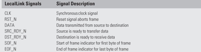
A transfer is initiated by the source by asserting the signals src_rdy_n and sof_n along with the first data word in the transfer. When the destination is ready to receive data it will assert dst_rdy_n. Only when both src_rdy_n and dst_rdy_n are asserted are data valid to the destination and should the source start to assert the next data word. Data are transferred in frames, with the start-of-frame and end-of-frame signals used as indicators to the beginning and end of the frame of data. The start-of-frame and end-of-frame signals should only be asserted during the transmission of the first and last byte of the frame, respectively.
In order to add a LocalLink interface to an existing hardware core we must add these signals to the entity description. Because LocalLink is unidirectional, if a hardware core is only sending data to a destination or only receiving data from a source, a single instance of the LocalLink ports is needed. In some cases there is a need for a hardware core to communicate either bidirectionally or receive data from a source and produce data to another destination. Under this circumstance, both transmit and receive LocalLink ports are needed. Keep in mind the directionality of the ports, that is, a source will transmit (output) data, start-of-frame, end-of-frame, and source ready signals, whereas the receiver will input these signals.
To help illustrate this point we will show how to add the LocalLink interface ports to an existing hardware core via the Microprocessor Description file. We will assume that the hardware core has two LocalLink ports, a transmit port and a receive port. Using the Xilinx bus standard XIL_LL_DMA to create bus interfaces, we must specify the transmit port as an initiator and the receive port as a target. In the Xilinx Platform Studio these two types result in a point-to-point bus that is similar to how the PLB Block RAM controller connects to the Block RAM component.
BUS_INTERFACE BUS = TX_LLINK0, BUS_STD = XIL_LL_DMA, BUS_TYPE = INITIATOR
BUS_INTERFACE BUS = RX_LLINK0, BUS_STD = XIL_LL_DMA, BUS_TYPE = TARGET
Connecting the LocalLink ports to the bus becomes fairly straightforward. The LocalLink bus standard connects transmit (source) ports to receive (destination) ports. As a result, the transmit ports for the hardware core are connected by default to the transmit ports of the LocalLink transmit bus. However, the receive ports are also connected to the transmit ports, but for the receive bus. This effectively crosses the transmit and receive signals to allow the receive port to input data that is output from the transmit port.
## LocalLink Transmit Port
PORT ll_tx_data = LL_Tx_Data, DIR = O, BUS = TX_LLINK0, VEC = [31:0]
PORT ll_tx_sof_n = LL_Tx_SOF_n, DIR = O, BUS = TX_LLINK0
PORT ll_tx_eof_n = LL_Tx_EOF_n, DIR = O, BUS = TX_LLINK0
PORT ll_tx_src_rdy_n = LL_Tx_SrcRdy_n, DIR = O, BUS = TX_LLINK0
PORT ll_tx_dst_rdy_n = LL_Tx_DstRdy_n, DIR = I, BUS = TX_LLINK0, INITIALVAL = VCC
# LocalLink Receive Port
PORT ll_rx_data = LL_Tx_Data, DIR = I, BUS = RX_LLINK0, INITIALVAL = GND, VEC = [31:0]
PORT ll_rx_sof_n = LL_Tx_SOF_n, DIR = I, BUS = RX_LLINK0, INITIALVAL = VCC
PORT ll_rx_eof_n = LL_Tx_EOF_n, DIR = I, BUS = RX_LLINK0, INITIALVAL = VCC
PORT ll_rx_src_rdy_n = LL_Tx_SrcRdy_n, DIR = I, BUS = RX_LLINK0, INITIALVAL = VCC
PORT ll_rx_dst_rdy_n = LL_Tx_DstRdy_n, DIR = O, BUS = RX_LLINK0
The LocalLink interface will be addressed shortly when we discuss a specific bus master implementation, although the Local-Link port is not connected through the MPD file because the bus master uses the LocalLink between components within the custom hardware core. The MPD file is used more directly in Chapter 7 when we implement interface components off of the FPGA.
6.B Off-Chip Memory Access
Accessing memory can be critical in a design and knowing how the memory can be accessed is an important design consideration. Throughout this section we aim to cover more specific details regarding various ways to access memory as well as different ways to interface with memory. Because memory bandwidth can be a precious commodity in systems design, being aware of the different memory access choices as a designer can affect the performance of the system.
6.B.1 Programmable I/O
The white pages presented a short C-code snippet that reads data from main memory and writes it to the compute core. Programmable I/O arguably provides the simplest interface between a hardware core and memory while requiring the least physical resources. This of course is at the expense of performance. The application may dictate how memory should be accessed. We only address the topic so as to alert readers to alternative solutions to accessing memory.
A specific Xilinx implementation for programmable I/O does not differ from the C-code already presented inbreak Chapter 6’s white pages. The requirement that both the memory controller and the hardware core are addressable by the processor means that both are slaves on a bus that the processor is a master on. It is possible that the memory controller and hardware core reside on two different buses, as long as the processor has access to both buses.
Because the objective of this chapter is to discuss different memory access methods, we focus our attention on these alternative approaches.
6.B.2 Central DMA Controller
An improvement on the performance of programmable I/O, where the processor performs the entire request, is to use a DMA controller. Xilinx provides a Central DMA Controller [Xilinx, Inc., 2009f] as a core in its EDK IP Core Repository. The processor issues a DMA request to the controller, which in turn handles the DMA transaction on behalf of the processor. The DMA controller can support:
• processor initiated read from memory and write to hardware core
• processor initiated read from hardware core and write to memory
• hardware core initiated read from memory and write to hardware core
• hardware core initiated read from hardware core and write to memory
It is important to understand that memory in the term “direct memory access” does not necessarily mean off-chip memory. In fact, transfers between the hardware core’s on-chip memory are also possible. We will discuss in more detail how a hardware core can initiate a request to the DMA controller shortly. For now, we will focus on how the central DMA controller works and, more specifically, will learn how to initiate a DMA request. Start by adding the central DMA controller to a previously created base system.
The central DMA controller includes both a master and a slave bus interface. The slave interface is for receiving DMA requests, for example, from the processor. The master interface is used to issue an actual memory request to the memory controller or compute core. The central DMA controller consists of a set of control registers used to set up the DMA request. In C, we can create a structure to access these registers more easily.
typedef struct{
unsigned int rst_reg; // Reset Register
unsigned int dmac_reg; // DMA Control Register
unsigned int sa_reg; // Source Address Register
unsigned int da_reg; // Destination Address Register
unsigned int len_reg; // Length Register
unsigned int dmas_reg; // DMA Status Register
unsigned int isr; // Interrupt Service Register
unsigned int ier; // Interrupt Enable Register
}cdma_regs;
To set up a DMA request, the processor will need to write into the source address register, destination address register, and, finally, the length register. The source address register is where the central DMA controller will read data from. The destination address is where read data will be written to. The length register contains the number of bytes to read from the source. The length register should always be written last because writing to it triggers the central DMA controller to begin the DMA request. Once the processor writes the length register it can either poll the DMA status register to determine when the request has completed or, if interrupts are used it can wait until the interrupt occurs to indicate the transaction has finished. In either case, the processor is free to perform any computation in parallel with the DMA transaction as long as the computation does not alter the contents of memory that is part of the DMA request until the transaction completes. We include a short C-code example here:
int main() {
// Central DMA Registers
volatile cdma_regs *cdma_core = (cdma_regs*)(CDMA_BASEADDR);
// Hardware Core Register(s) - Can be any interface
volatile hw_regs *hw_core = (hw_regs*)(HWCORE_BASEADDR);
// Data located in memory to be read by DMA Controller
volatile unsigned int data[TEST_SIZE];
int i;
// Write Data into Memory
for(i=0;i<TEST_SIZE;i++) {
data[i] = i;
}
// Set DMA Source Addresses
cdma_core->sa_reg = (unsigned int) &data[0];
printf(“Source Reg = 0x%08x ”, cdma_core->sa_reg);
// Set DMA Destination Addresses
cdma_core->da_reg = (unsigned int) &hw_core->slv_reg0;
printf(“Dest Reg = 0x%08x ”, cdma_core->da_reg);
// Set DMA Length Register & Start DMA Transfer
cdma_core->len_reg = TEST_SIZE * sizeof(int);
printf(“Length Reg = 0x%08x ”, cdma_core->len_reg);
// Perform Parallel Computation - if any
// Verify Results - Read from Slave Register
printf(“slv_reg0 = 0x%08x ”, hw_core->slv_reg0);
printf(“Test Complete ”);
}
In order to receive burst transactions from the DMA controller, the hardware core must be set to support burst and cache-line transfers. This can be done when creating the hardware core through the Create and Import Peripheral Wizard that is part of the Xilinx EDK. Without this support, only single transfers can be made to the core.
The central DMA controller is a useful tool in offloading memory requests from the processor. The example just given illustrates this by transferring data from memory to a slave register on a hardware core. The final printf statement should reveal the contents of slv_reg0 to be the last element transmitted from memory. Because each application’s need differs, we assume that writing to this single port is sufficient.
6.B.3 Bus Master
Adding bus master capability to a hardware core can further improve performance by allowing the core to issue its own memory requests rather than relying on the processor and DMA controller. It is still possible to integrate a bus master hardware core with the central DMA controller; however, it would be more efficient for the hardware core to directly issue memory requests to the memory controller rather than have the DMA controller act as a middleman. This is due to the fact that the DMA controller requires at least three separate bus transfers to set the source, destination, and length registers, whereas the bus master can issue a single request to the memory controller.
Because each bus implementation differs, we will continue to use the Processor Local Bus (PLB) for our demonstrations. Starting with the Xilinx Create and Import Peripheral Wizard, refer back to Section 2.A; we can add bus master support with an additional check box, “User Logic Master.” This will generate a template for a master interface on the PLB. To better understand how the master works, we will look at the new interface signals and logic added to the user_logic.vhd file.
Bus Master Signals
The Xilinx IP Interconnect (IPIC) (listing in Table 6.2) is used to help reduce the number of signals the hardware core needs to interface with when issuing requests across the PLB. The hardware core can be a bus slave, bus master, or both a slave and a master. Because we have covered a bus slave already, we will focus our attention on the master signals, which are denoted by _Mst in the signal name. Signals beginning with IP2Bus_ indicate an output signal from the entity to the bus. Signals beginning with Bus2IP_ indicate an input signal coming from the bus into the entity. Signals ending with _n indicate negative logic signals.
Table 6.2
Xilinx IPIC signals for PLB master.
| IPIC Signals | Signal Description |
| Bus2IP_Mst_CmdAck | Bus Command Acknowledgment |
| Bus2IP_Mst_Cmplt | Bus Transfer Complete |
| Bus2IP_Mst_Error | Bus Error |
| Bus2IP_yMst_Rearbitrate | Bus Rearbitrate |
| Bus2IP_yMst_Cmd_Timeout | Bus Command Timeout |
| IP2Bus_MstRd_Req | Issue a Master Read Request |
| IP2Bus_yMstWr_Req | Issue a Master Write Request |
| IP2Bus_yMst_Addr | Address to Read or Write Data |
| IP2Bus_Mst_BE | Write Data Byte Enable |
| IP2Bus_Mst_yLength | Number of Bytes for Request |
| IP2Bus_Mst_yType | Transfer Type |
| IP2Bus_Mst_Lock | Lock Bus during Transaction |
| IP2Bus_Mst_Reset | Issue a Bus Reset |
| Bus2IP_yMstRd_d | LocalLink Read Data |
| Bus2IP_yMstRd_rem | LocalLink Read Data Remainder |
| Bus2IP_MstRd_ysof_n | LocalLink Read Start of Frame |
| Bus2IP_MstRd_eof_n | LocalLink Read End of Frame |
| Bus2IP_MstRd_src_yrdy_n | LocalLink Read Source Ready |
| Bus2IP_yMstRd_src_dsc_n | LocalLink Read Source Discontinue |
| IP2Bus_MstRd_ydst_rdy_yn | LocalLink Read Destination Ready |
| IP2Bus_MstRd_ydst_dsc_n | LocalLink Read Destination Discontinue |
| IP2Bus_MstWr_d | LocalLink Write Data |
| IP2Bus_yMstWr_rem | LocalLink Write Data Remainder |
| IP2Bus_yMstWr_sof_n | LocalLink Write Start of Frame |
| IP2Bus_MstWr_eof_yn | LocalLink Write End of Frame |
| IP2Bus_MstWr_ysrc_rdy_n | LocalLink Write Source Ready |
| IP2Bus_MstWr_src_ydsc_n | LocalLink Write Source Discontinue |
| xBus2IP_yMstWr_dst_rdy_n | LocalLink Write Destination Ready |
| Bus2IP_MstWr_dst_dsc_n | LocalLink Write Destination Discontinue |
From these lists we can see there are more than just input and output signals. In fact, there are two other groups of signals. The first group contains the LocalLink signals, which follow the LocalLink specification for transmitting data to and from the hardware core. Because LocalLink is a unidirectional specification and we want to support bidirectional transfers, read and write transfers, there are two sets of LocalLink signals in the master interface.
The second group contains the bus control signals. As with the LocalLink signals there are two directions: input from the bus and output from the hardware core. On the bus side are command acknowledgment, transfer complete, error, arbitrate, and command timeout signals. These signals are used to relay bus information to the hardware core. If the bus needs the hardware core to reissue a request, it will assert the bus rearbitrate signal. On the hardware core side are read request, write request, address, data byte enable, length, type, lock, and reset signals. The hardware core asserts these signals to indicate a read request from a specific address and, if the request is a burst request, the length of the transfer. These are considered the control signals for the bus transaction.
Bus Master Logic
Now that we have a better idea of what the bus master interface signals are, we will look at the master logic within the user_logic.vhd file. The template provided by Xilinx includes three finite state machines for the bus master. One state machine is for the LocalLink read requests. The second state machine is for the LocalLink write requests. The third state machine acts as a controller over the bus requests and read and write state machines.
Xilinx also provides a set of master registers to allow simple testing with a software application. Because each application may differ in how the bus master is driven (by a software application, by a custom finite state machine, etc.), we will instead focus on the three finite state machines and allow readers to experiment with alternative interfaces to the master control registers. Comments generated by the Xilinx wizard provide a helpful starting point for software-based master requests. In our experience, once the three state machines are understood, augmenting them to meet the needs of the design is trivial.
For those familiar with the earlier version of the Xilinx EDK software, the tools prior to version 10.1 did not include a LocalLink interface. The older master interface relied on the instantiation of a bus slave with the bus master to support transfers to and from the hardware core. Since version 10.1, this has been replaced with the LocalLink interface. Now the hardware core does not need to instantiate a bus slave if only a bus master is required, resulting in fewer resources being used whenever possible.
Control Finite State Machine
We have briefly discussed a finite state machine for the bus master, which interacts with the bus control signals and the read and write finite state machines. For more details regarding the control finite state machine, see Figure 6.16.

Figure 6.16 Bus master control finite state machine.
The CMD_IDLE state waits for either a read or a write request (this can be from the master control register provided by the template or a custom finite state machine). Once a read or write request has been issued, the corresponding LocalLink finite state machine is started and then transitions into the CMD_RUN state.
To indicate that the request has been received by the bus interface, the Bus2IP_Mst_CmdAck (command acknowledgment) signal is asserted. This also notifies the control finite state machine to deassert the bus request signals because the request is in transit and keeping the signals asserted risks issuing a second identical request. In the event a timeout or error occurs, the control finite state machine should respond based on the requirements of the system. The template asserts status signals to be read by the software application. This may suffice for your application or more logic may be necessary to support reissuing the request.
When the command acknowledgment signal is asserted it may be asserted with the Bus2IP_Mst_Cmplt (command complete) signal. The command complete signal indicates that all requested data have been transferred to or from the hardware core. If both signals are asserted at the same time, the control finite state machine should transition to the CMD_DONE state. Under some circumstances the command acknowledgment signal is asserted without the command complete, in which case the control finite state machine can deassert the request signals, but must wait for the command complete signal. This is done in the CMD_WAIT_FOR_DATA state. Finally, the CMD_DONE state returns to the CMD_IDLE state to wait for the next request.
Read Request Finite State Machine
The read request finite state machine controls read requests where data are read from a core on the bus and returned to the hardware core via the read LocalLink interface signals. Because data are being delivered to the hardware core there are only a few signals to interact with. The read request is triggered by the control finite state machine, so until a read request is asserted the default state is the LLRD_IDLE state. Once a request is asserted the read request finite state machine transitions to the LLRD_GO state. In this state, when both the Bus2IP_MstRd_src_rdy_n (source ready) and the IP2Bus_MstRd_dst_rdy_n (destination ready) signals are asserted, data are flowing from the source to the destination. The hardware core can pause the transfer by deasserting the IP2Bus_MstRd_dst_rdy_n signal. This can be useful in streaming applications where data arrive after they can be processed or data are written into a FIFO for internal buffering and the buffer becomes full. The read request completes when the Bus2IP_MstRd_eof_n (end-of-frame) signal is asserted, meaning that the last word in the transfer has arrived. The read request finite state machine returns to the LLRD_IDLE state waiting for the next read request. Figure 6.17 illustrates the LocalLink read request finite state machine.

Figure 6.17 Bus master read request finite state machine.
Write Request Finite State Machine
The write request finite state machine controls write requests where data are written from the hardware core to another core on the bus via the write LocalLink interface signals. Similar to the read request finite state machine, the write request finite state machine waits in the LLWR_IDLE state until a write request is issued. If burst transfers are supported, allowing more than a single word of data to be transmitted per each transaction, then the next state can be either LLWR_BURST_INIT or LLWR_SNGL_INIT, indicating a burst or single transaction.
During a single word write transaction the write request finite state machine must wait until both the destination and the source are ready, as indicated by the Bus2IP_MstWr_dst_rdy_n and IP2Bus_MstWr_src_rdy_n signals. At this time both the IP2Bus_MstWr_sof_n and the IP2Bus_MstWr_eof_n signals must be asserted as well to signify that the LocalLink transfer is a single word. The write request finite state machine can then return to the LLWR_IDLE to wait for the next write request.
Conversely, a burst write transaction requires the write finite state machine to issue multiple words of data to the destination core. The transfer length is identified by IP2Bus_MstWr_Length. A burst transfer must still adhere to the requirement that a valid transfer requires both source and destination ready signals to be asserted. The start-of-frame signal must be asserted during the transfer of the first word in the burst, while the end-of-frame signal must be asserted during the transfer of the last word. A counter can be used to help keep track of the amount of data left to be transferred in the burst transaction. A last state LLWR_BURST_LAST_BEAT is used to assert the end of frame accordingly. When the transfer completes, the write finite state machine returns to the LLWR_IDLE to wait for the next write request. Figure 6.18 illustrates the LocalLink write request finite state machine.

Figure 6.18 Bus master write request finite state machine.
Adding bus master support to a hardware core can enhance the functionality of the hardware core greatly, allowing it to act much more independently than when just a bus slave. Not all applications may require this functionality; however, understanding how it is implemented is a useful design tool.
6.B.4 Native Port Interface
When hardware cores need high bandwidth and low latency transfers to off-chip memory, Xilinx provides a custom interface to their Multi-Ported Memory Controller (MPMC) known as the Native Port Interface (NPI). This is different than a bus master in that it is a direct connect interface to the memory controller instead of a connection to a shared bus. Because the interface is not shared it does not require arbitration, allowing for lower latency transfers. Also, due to the direct connection, the hardware core can receive data at the memory controller’s operating frequency, which can be higher than the bus operating frequency, providing a higher bandwidth.
Unlike the bus master, Xilinx does not directly support NPI integration into a hardware core through generated templates. This may change in future releases of the tools, but as of now the designer is required to make some modifications to a hardware core needing the NPI. Also, the NPI does not follow the LocalLink standard. If there is a need to use the LocalLink interconnect, the MPMC already supports the LocalLink directory through the SDMA port. However, the LocalLink interface is limited to a maximum data width of 32 bits. With NPI we can operate at 64-bit widths for ![]() the bandwidth.
the bandwidth.
NPI Signals
First we must discuss the signals used by the native port interface, shown in Table 6.3. These signals will need to be added to the hardware core’s entity port listing. The interface consists of three groups of signals. The first group contains the request and control signals: clock, reset, address, address request, address acknowledgment, read-not-write, size, read-modify-write, and initialize done. The second group contains the write FIFO signals, which transfer data out to the MPMC. The last group contains the read FIFO signals, which bring in data from the MPMC.
Table 6.3
Xilinx Native Port Interface signals.
| NPI Signals | Direction | Signal Description |
| XIL_NPI_CLK | IN | Clock |
| XIL_NPI_RST | IN | Reset |
| XIL_NPI_Addr | OUT | 32-bit Address |
| XIL_NPI_AddrReq | OUT | Address Request |
| XIL_NPI_AddrAck | IN | Address Request Acknowledgment |
| XIL_NPI_RNW | OUT | Request Type Request |
| XIL_NPI_Size | OUT | Request Size (Burst or Single) |
| XIL_NPI_RdModWr | OUT | Read Modify Write |
| XIL_NPI_InitDone | IN | Memory Initialization Done |
| XIL_NPI_WrFIFO_Data | OUT | 64-bit Data Output |
| XIL_NPI_WrFIFO_BE | OUT | 8-bit Data Output Byte Enable |
| XIL_NPI_WrFIFO_Push | OUT | Data Output Write Enable |
| XIL_NPI_WrFIFO_Empty | IN | Data Output FIFO Empty |
| XIL_NPI_WrFIFO_AlmostFull | IN | Data Output FIFO Almost Full |
| XIL_NPI_WrFIFO_Flush | OUT | Data Output FIFO Flush (Reset) |
| XIL_NPI_RdFIFO_Data | IN | 64-bit Data Input |
| XIL_NPI_RdFIFO_Pop | OUT | Data Input Read Enable |
| XIL_NPI_RdFIFO_RdWdAddr | IN | 4-bit Read Write Address |
| XIL_NPI_RdFIFO_Empty | IN | Data Input FIFO Empty |
| XIL_NPI_RdFIFO_Flush | OUT | Data Input FIFO Flush (Reset) |
| XIL_NPI_RdFIFO_Latency | IN | 2-bit Read FIFO Latency Indicator |
The clock signal must be the same clock connected to the MPMC. We will discuss how to connect this clock along with connecting the hardware core to the MPMC shortly. The read and write FIFOs exist physically within the MPMC. The NPI signals interact with these FIFOs. It is not necessary to instantiate separate read and write FIFOs within your hardware core, except when required by the design.
NPI Little Endian
The native port interface and multi-port memory controller data are little endian, which may be in conflict with the application running on the Xilinx PowerPC (which can interface with memory as big endian). As a result, it may be necessary to do an endian swap when reading data from and writing data to memory. This can be accomplished through byte aligning, which simply flips the bytes from one endian to the other.
INPUT_ENDIAN_SWAP_PROC: process ( NPI_RdFIFO_Data ) is
begin
data_from_mem(0 to 7) <= NPI_RdFIFO_Data(7 downto 0);
data_from_mem(8 to 15) <= NPI_RdFIFO_Data(15 downto 8);
data_from_mem(16 to 23) <= NPI_RdFIFO_Data(23 downto 16);
data_from_mem(24 to 31) <= NPI_RdFIFO_Data(31 downto 24);
data_from_mem(32 to 39) <= NPI_RdFIFO_Data(39 downto 32);
data_from_mem(40 to 47) <= NPI_RdFIFO_Data(47 downto 40);
data_from_mem(48 to 55) <= NPI_RdFIFO_Data(55 downto 48);
data_from_mem(56 to 63) <= NPI_RdFIFO_Data(63 downto 56);
end process INPUT_ENDIAN_SWAP_PROC;
NPI Data Transfers
The NPI request transfer size (length) is set with XIL_NPI_Size, which encodes the number of bytes to read or write in a 4-bit signal. The smallest transfer consists of a data word, while the largest is fixed to 16 words. This is the same limitation set on the bus master for a single transaction, except with the bus master the length signal specifies the number of bytes to transfer. Because we are using the NPI to transfer 64-bit data words (8 byte), the smallest transfer is 8 Bytes and the largest is 128 Bytes. Table 6.4 lists the encoding for XIL_NPI_Size necessary to transfer the specific number of bytes. It is possible to transfer less than 8 Bytes through the use of the XIL_NPI_WrFIFO_BE (byte enable) signal along with the XIL_NPI_RdModWr (read-modify-write) signal. We will discuss how to accomplish this shortly.
Table 6.4
Native Port Interface data transfer size encoding.
| XIL_NPI_Size | Bytes Transferred |
| 0000 | 8 |
| 0001 | 16 |
| 0010 | 32 |
| 0011 | 64 |
| 0100 | 128 |
With burst transfers, the latency of the first word is the longest, then every consecutive word thereafter arrives one clock cycle after the previous word. As mentioned in Section 6.2, we can improve the performance through the use of double buffering. This is more useful for read requests, which are covered in the next section.
One additional constraint NPI imposes on burst transfers is on the address (XIL_NPI_Addr), which must be aligned to the transfer size. That is, each address must be on the boundary of the transfer length. For a single word transfer the address must end with 0x0 or 0x8, meaning aligned to the 8-Byte boundary. For a double word transfer the address must end with 0x0 or a multiple of 0x10 and so forth up to the 128-Byte boundary, requiring the address to end in 0x00 or 0x80.
NPI Logic
Because each hardware core may need to interact with the NPI differently, for brevity, we will just cover the logic necessary to instantiate the NPI. Whether the design calls for integrating the NPI into a Xilinx-generated hardware core on the PLB or another custom core, this NPI instantiation information is targeted toward how to use the NPI. Adding higher levels of control (as is done with the bus master template via the software addressable master control register) is left to the individual implementation of the design.
To begin, add the NPI signals to the entity list of the hardware core being designed. Be sure to match the direction and bit vector widths accordingly (if there is no indication of the width, assume 1 bit). After we discuss the necessary logic required to implement the NPI, we will explain how to modify the MPD file and connect the NPI to the MPMC within Xilinx Platform Studio.
As with the bus master, we will use three finite state machines to perform memory transactions with NPI. The control finite state machine will be used to issue requests to the memory controller. The read request finite state machine will handle receiving data from the memory controller. The write request finite state machine will handle writing data to the memory controller. We divide the NPI logic into these three functionalities in order to support parallel transactions. While it is not possible to issue a read and a write request at the exact same time, it is possible to issue one request and, once acknowledged, issue a second request. Depending on the application, this may or may not be necessary; however, with the desired goal of designing a high bandwidth interface to memory, supporting as many parallel operations as possible will help us achieve our goal.
Control Finite State Machine
Unlike the bus master control finite state machine where only one read or write request can be in process at a time, we have implemented the NPI control finite state machine to support nearly parallel transfers of read and write requests. We say nearly because we are not able to support the starting two requests concurrently. We can issue one request directly followed by a second request (while the first request is still being processed). To support this functionality we have moved much of the read and write control logic to the read and write request finite state machines, respectively. The result is a simpler two state control finite state machine, as seen in Figure 6.19.
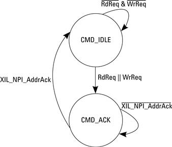
Figure 6.19 Native Port Interface control finite state machine.
The control finite state machine waits in the CMD_IDLE state until a request is issued by either the read or the write request finite state machine. When a request is received, the control finite state machine passes the request on to the MPMC. The request signals include the address, type (read or write request), and transfer size.
The control finite state machine transitions to the CMD_ACK state, waiting for the XIL_NPI_AddrAck signal. The address acknowledgment indicates that the MPMC has received the request and is beginning to process the request. During this same clock cycle the NPI control finite state machine must deassert the request signals and return to the CMD_IDLE state so as to not unintentionally issue a second identical request.
In the event that both a read and a write request signal are received by the control finite state machine at the same time, a priority is set to issue read requests before write requests to support designs needing low-latency reads from memory and to avoid stalls in the computation. Of course the two requests are still able to be issued nearly in parallel since once request will still be in process while the other request can be made.
Read Request Finite State Machine
The read request finite state machine waits for a request from some external component (or controlling mechanism). We have specifically chosen not to build the issuing read request logic into these examples because it is very application specific. As with the bus master, it is possible to include a control register to trigger read and write requests or design any number of custom components. Instead we focus our efforts on the finite state machines needed to interact with the native port interface and multiport memory controller. Because we have moved the request logic out of the control finite state machine and into both read and write request finite state machines, we need to begin by explaining how these state machines are integrated.
The read request finite state machine (Figure 6.20) waits in the RD_IDLE state until it receives a start signal to issue a read request. Once the request is received the read request finite state machine transitions to the RD_ISSUE_REQ state, where it passes the request to the control finite state machine. The control finite state machine is actually where the requests are issued to the MPMC. The read request finite state machine waits in this state until the request has been acknowledged by the MPMC, indicating that data will be returned shortly to the NPI. Once the acknowledgment is received, the state machine transitions to the RD_WAIT_FOR_DATA state.

Figure 6.20 Native Port Interface read request finite state machine.
The data’s arrival to the NPI is indicated through deassertion of the XIL_NPI_RdFIFO_Empty signal. Data are buffered in a read FIFO (RdFIFO) within the MPMC to allow the NPI to read data at its convenience through the use of XIL_NPI_RdFIFO_Pop. There is a read latency associated with the RdFIFO. It is a fixed latency (although the requests can be pipelined), which is denoted by XIL_NPI_RdFIFO_Latency. The latency depends on the parameters of the MPMC and because it is not possible to pass parameters between independent cores, it must be issued as a signal. This 2-bit signal is also necessary because there is no data valid signal to indicate when data from the FIFO are valid. If the latency is two clock cycles, then when the XIL_NPI_RdFIFO_Pop is first asserted to retrieve data (assuming the RdFIFO is not empty) the first data will be valid after two clock cycles.
The transfer is finished when the XIL_NPI_RdFIFO_Empty signal is asserted. Therefore, the read request finite state machine transitions to RD_DONE to signify that the transfer is done, followed by transitioning back to the RD_IDLE state to wait for the next request.
To achieve a high bandwidth, consecutive read requests can be issued to the MPMC, as long as the RdFIFO does not become full, which poses a risk of losing data. With each transaction being limited to a maximum of 128 Bytes, any larger transfers must be split into multiple smaller transfers no larger than 128 Bytes each. These transfers can be chained together and issued one after the other.
Write Request Finite State Machine
The write finite state machine (Figure 6.21) operates similarly to the read finite state machine in that it waits in the WR_IDLE state for a start signal to trigger a write request. Unlike a read request, which waits for data to arrive in the RdFIFO, a write request must first store data into the Write FIFO (WrFIFO) and then issue the request to the MPMC. The reason is that the MPMC assumes when it receives a write request that all data to be transferred are already stored in the WrFIFO.

Figure 6.21 Native Port Interface write request finite state machine.
In the event of a single transfer the write request finite state machine must issue a single word transfer, done in the WR_SNGL state. This requires asserting the XIL_NPI_RdModWr (read-modify-write) signal. Working with the XIL_NPI_WrFIFO_BE (byte enable) signal, if writing less than 8 Bytes, data must be read from memory and then modified and written back. The read-modify-write signal must be asserted with the address and address request signals after data have been written to the WrFIFO.
If the transfer is a burst request, data need to be written first to the WrFIFO followed by issuing the write request. This is done in the WR_BURST state. The address must also be aligned to the transfer size to avoid unpredictable performance (such as writing to the wrong address range). The size of the burst is specified by the XIL_NPI_Size signal. If a request does not fit within these burst sizes, it must be split into smaller requests. For example, writing a total of 88 Bytes would require a burst of 64 Bytes plus 16 Bytes plus a final transfer of 8 Bytes. This problem is further complicated by the need to align the address on the data boundary. A simple write request finite state machine can ignore these requests and pass the requirement on to the component issuing the requests (which could be the processor or some other compute core). A more complicated solution would involve the write request finite state machine managing these requirements. For now we rely on the request to be aligned properly.
Regardless of the transfer type, the next state, WR_WAIT_FOR_ACK, waits until the MPMC acknowledges the request. Once the acknowledgment is received the write request finite state machine deasserts the request and transitions to the WR_DONE state, signaling that the transfer has finished, and returns to the WR_IDLE state.
NPI Microprocessor Peripheral Description
After the NPI logic has been written and tested in simulation, it is time to modify the microprocessor peripheral description (MPD) file. We do this to support connectivity between the hardware core and MPMC in Xilinx Platform Studio. We start with the bus interface, which indicates that the NPI signals are part of the XIL_NPI bus standard.
## Bus Interfaces
BUS_INTERFACE BUS = XIL_NPI, BUS_TYPE = INITIATOR, BUS_STD = XIL_NPI
Now all of the NPI ports can be added and associated with XIL_NPI bus. These are all of the necessary NPI ports that are listed in the hardware core entity description. The default assignment is used to connect each signal to the corresponding bus signal. If left unassigned, the signal will be unconnected during PlatGen, potentially resulting in a synthesis error.
## Ports
PORT XIL_NPI_Addr = “Addr”, DIR = O, VEC = [31:0], ENDIAN = LITTLE, BUS = XIL_NPI
PORT XIL_NPI_AddrReq = “AddrReq”, DIR = O, BUS = XIL_NPI
PORT XIL_NPI_AddrAck = “AddrAck”, DIR = I, BUS = XIL_NPI
PORT XIL_NPI_RNW = “RNW”, DIR = O, BUS = XIL_NPI
PORT XIL_NPI_Size = “Size”, DIR = O, VEC = [3:0], BUS = XIL_NPI
PORT XIL_NPI_WrFIFO_Data = “WrFIFO_Data”, DIR = O, VEC = [63:0], ENDIAN = LITTLE, BUS = XIL_NPI
PORT XIL_NPI_WrFIFO_BE = “WrFIFO_BE”, DIR = O, VEC = [7:0], ENDIAN = LITTLE, BUS = XIL_NPI
PORT XIL_NPI_WrFIFO_Push = “WrFIFO_Push”, DIR = O, BUS = XIL_NPI
PORT XIL_NPI_RdFIFO_Data = “RdFIFO_Data”, DIR = I, VEC = [63:0], ENDIAN = LITTLE, BUS = XIL_NPI
PORT XIL_NPI_RdFIFO_Pop = “RdFIFO_Pop”, DIR = O, BUS = XIL_NPI
PORT XIL_NPI_RdFIFO_RdWdAddr = “RdFIFO_RdWdAddr”, DIR = I, VEC = [3:0], ENDIAN = LITTLE, BUS = XIL_NPI
PORT XIL_NPI_WrFIFO_Empty = “WrFIFO_Empty”, DIR = I, BUS = XIL_NPI
PORT XIL_NPI_WrFIFO_AlmostFull = “WrFIFO_AlmostFull”, DIR = I, BUS = XIL_NPI
PORT XIL_NPI_WrFIFO_Flush = “WrFIFO_Flush”, DIR = O, BUS = XIL_NPI
PORT XIL_NPI_RdFIFO_Empty = “RdFIFO_Empty”, DIR = I, BUS = XIL_NPI
PORT XIL_NPI_RdFIFO_Flush = “RdFIFO_Flush”, DIR = O, BUS = XIL_NPI
PORT XIL_NPI_RdFIFO_Latency = “RdFIFO_Latency”, DIR = I, VEC = [1:0], BUS = XIL_NPI
PORT XIL_NPI_RdModWr = “RdModWr”, DIR = O, BUS = XIL_NPI
PORT XIL_NPI_InitDone = “InitDone”, DIR = I, BUS = XIL_NPI
PORT XIL_NPI_Clk = “Clk”, DIR = I, BUS = XIL_NPI
PORT XIL_NPI_Rst = “Rst”, DIR = I, BUS = XIL_NPI
Xilinx Project Modifications
With all of the modifications to the HDL and MPD file it is now possible to connect the hardware core to the MPMC in the Xilinx Platform Studio. To do this the MPMC must first be modified to include an additional port of type NPI.
From within XPS, under the System Assembly View, select the MPMC (by default the instance name is DDR2_SDRAM_DIMM0 for ML-510 base systems) and choose Configure IP.
The MPMC supports up to eight ports. The default configuration is for Port 0 to be configured as PLBV46. What this means is that Port 0 can be connected as a slave to a single instance of the Processor Local Bus. We need to add a second port of type NPI. Once set, our MPMC will resemble Figure 6.22.
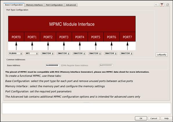
Figure 6.22 Xilinx Multi-Port Memory Controller configured with two ports: PLB and NPI.
Close the MPMC configuration window and expand MPMC interfaces to see SPLB0 connected to plb_v46_0 and MPMC_PIM1 listed as No Connection. Selecting the drop-down menu, we can change the connection to the NPI bus of the hardware core.
An important note regarding ML-510 designs: by default the Base System Builder wizard sets the memory controller for DIMM0 to the PPC440 Memory Controller. This is not the same as the Multi-Port Memory Controller. With this memory controller you will not be able to add additional ports, such as the Native Port Interface.
As is evident by the amount of material covered within this section, there are a wide variety of ways to not only implement memory, but access memory as well. It is hoped that these examples act as a catalyst to explore and develop efficient memory access interfaces within your designs. Whether implementing the simpler programmable I/O interface, using a central DMA controller, or supporting memory access from within the hardware core, it is necessary to recognize the trade-offs between resources and performance.
Exercises
P6.1. Considering Figure 6.1, if the amount of time to perform a multplication was reduced by a factor of 2, draw the corresponding system, including any necessary buffers to maintain a pipeline balance.
P6.2. Draw the interface between two components where one is producing data and the second is consuming data. Be sure to follow the Kahn Process Network model.
P6.3. Describe the similarities and differences between synchronous and asynchronous design.
P6.4. Draw the interface for a FIFO. Compare this interface to that of a BRAM.
P6.5. Write the VHDL that will instantiate a BRAM and function like a FIFO. Include in this design a mechanism to report to the user the number of elements currently stored in the FIFO.
P6.6. Write an application that will use the Central DMA controller to read 512 Bytes of data from DDR2 and write it to a hardware core. Assume data are stored at 0x0123000 and must be written to 0xB001000.
P6.7. Compare the performance of a system that is operating in CMDA mode with that of a system running as a bus master that is able to access memory on its own.
P6.8. Implement a Native Port Interface design that will support direct memory access reads and writes to the MPMC without the aid of the processor.
References
1. Kahn G. The semantics of simple language for parallel programming. In: Rosenfeld JL, ed. Information Processing ’74 (pp 471–475). Amsterdam: North Holland; 1974.
2. Xilinx, Inc. LocalLink interface specification (SP006) v2.0 San Jose, CA: Xilinx, Inc. 2005.
3. Xilinx, Inc. Answer record 24912 — 11.1 EDK, MPMC v5.00.a — How do I create an NPI Core and connect it to MPMC in EDK? 2009a; http://www.xilinx.com/ last accessed June 2010.
4. Xilinx, Inc. Block memory generator data sheet (DS512) v3.3 San Jose, CA: Xilinx, Inc. 2009b.
5. Xilinx, Inc. Distributed memory generator (DS322) v4.3 San Jose, CA: Xilinx, Inc. 2009c.
6. Xilinx, Inc. FIFO generator data sheet (DS317) v5.3 San Jose, CA: Xilinx, Inc. 2009d.
7. Xilinx, Inc. Multi-port memory controller (MPMC) v5.04.a San Jose, CA: Xilinx, Inc. 2009e.
8. Xilinx, Inc. XPS central DMA controller (DS579) v2.01b San Jose, CA: Xilinx, Inc. 2009f.