
Chapter 5
Advanced Magnetics
Optimal Core SelectionThis chapter is a recap of the basics, progressing on to advanced magnetics. It starts by explaining the grass-root differences in the underlying energy transfer process between the three fundamental topologies. It shows how the size of their inductors varies for a given output power based on duty cycle and topology. The concept of magnetic circuits with the distribution of the B and H fields in gapped and ungapped cores is introduced along with derivations of the equations for energy storage capability. The innovative “air gap factor” is introduced, which greatly simplifies and aids a typical power conversion engineer’s understanding of gapped magnetic cores. The morphing of E-cores into toroids is shown by a unique “comic-strip” diagram, so that a given calculated air gap can be correctly set in practice. Then, based on all the principles and equations presented thus far, a detailed numerical example is presented for optimal core size selection and air gap setting in a universal input AC/DC flyback. Finally, the equations for skin depth and proximity losses corresponding to rectangular waveforms, based on Dowell’s historic equations for sine waves, are derived and plotted out, for optimizing AC–DC Forward converter transformer designs.
Part 1: Energy Transfer Principles
Overview of Topologies
We will now progress from the concepts presented in preceding chapters and develop expertise to optimize the energy storage sections of DC–DC switching power converter stages, with special attention to their magnetics.
We recapitulate briefly first. A switching topology has three key power components.
(a) An inductor in which the current undulates every cycle between two levels of current. These levels remain fixed in “steady state,” that is, when power-up is complete and no changes in line or load are occurring.
(b) A switch connected to the inductor, which turns ON and OFF every cycle. Typically the ON-time interval starts under command of the clock, and the OFF-time is initiated under the command of the error-amplifier/feedback-loop.
(c) A catch (“freewheeling”) diode connected to both the switch and inductor at a common node, called the “switching (or swinging) node.” The diode gets reverse-biased whenever the switch is ON and forward-biased whenever the switch turns OFF.
The switch and diode have complementary actions: when one is ON, the other is OFF and vice versa. The purpose is to alternate the inductor current between the switch and diode, so that it always has a path to flow in. Otherwise the converter would get destroyed by the resulting voltage spike (see Figure 1.6 again).
In all topologies, when the switch conducts, it associates the inductor with the input voltage source. And whenever the diode conducts (i.e., when switch is OFF), it associates the inductor with the output (load). Therefore, during the ON-time, energy flows into the converter through the switch. Here we keep in mind that current always flows in a complete loop, but delivers energy only when there is a potential difference, since work done is, by definition, potential difference multiplied by current. The increase in energy during the ON-time manifests itself as current ramping up linearly in the inductor and the switch. Similarly, during the OFF-time, inductor current flows through the diode, which conducts, and thereby establishes a path to the output. So, the converter pushes energy out into the load during the OFF-time, and the resulting decrease in inductor energy manifests itself as current ramping down linearly in the inductor and the diode.
The relationship between current and energy levels in the inductor is expressed by the basic relationship
![]()
One of the key questions in magnetics design is: what should the optimum value of L (i.e., the inductance) be? We already know from previous chapters that the choice of L usually depends on a very simple and almost universal criterion — that of achieving ±20% current ripple (r=0.4) at max load. The total swing ΔI per cycle is then 40% of the average DC value (i.e., the center of ramp). But anyway, selecting L is only a secondary concern. The first step in any magnetics design process, and the most important and difficult question to answer is: what core size should we pick? It is energy that is the key to answering that, since we are talking about power conversion, and power is, by definition, energy per second. So, once we understand energy, we can ensure we have sized the bulky energy storage components (the inductor and the input and output capacitors) correctly to handle the energy coming their way, and at the rate at which it will come. And once we know how much energy is flowing through each stage of the converter, we can determine how much of that gets dissipated (wasted) en route, inside the switch and the diode for example. This helps us pick the power semiconductors correctly, so they do not get too hot for example. And that in turn leads us into the area of thermal management — the heatsinking, air speed, and so on. In brief, energy underlines everything that is not control loop design. And it is very important, because unlike control loop design, energy largely determines size and cost of the converter, and also determines the overall system reliability. We therefore need to understand energy as well as control loop theory if not better — especially in today’s “green era.”
Keep in mind the relationship between Watts and Joules. As mentioned, Watts is Joules per second or J/s or J s–1. Hertz (Hz) is cycles per second, or 1/s, or s−1 since “cycle” is dimensionless. As an example, if we have a converter switching at 100 kHz, with an output power rating of 50 W, the energy output per cycle, which we are calling εO (expressed in Joules per cycle, or simply Joules) is
![]()
If we pick a switching frequency of 1 MHz, the energy output per cycle would be only 50 μJ, leading to smaller magnetics for the same output power. If the efficiency was say 80%, the input power would be 50 W/0.8=62.5 W. The energy drawn from the input per cycle would then be 62.5 μJ for a switching frequency of 1 MHz, or 625 μJ per cycle for a frequency of 100 kHz. All this takes us back to the train terminus analogy on Page 1 of this book, where we mentioned how energy flows into a converter continuously, leaves continuously, but en route gets chopped into packets, the size of which depends on how quickly we move the trains in and out. Another way of visualizing the Joules–Watts relationship is as follows: if we are able to process 50 μJ per event, and we repeat that event a million times, we will get 50×106 μJ, that is, 50 J. Now, if we complete those million identical events (cycles) in exactly 1 s, that would be a frequency of 1 MHz, and we get 50 J/s, or 50 W by definition. So, we have 50 W being processed, at a switching frequency of 1 MHz. However, if we had completed those million cycles at a much slower pace, say in 10 s, we would get only 50/10=5 J coming out per second, which is 5 W, at a switching frequency of 106 cycles/10 s=105 Hz, that is, 100 kHz.
In determining core sizes for use in switching power supply design, there is an underlying “topology dependency” that is often overlooked in related literature. We will now uncover this so that we can select cores more optimally.
We mentioned that during the ON-time, energy flows from the input source to the converter. Where does it go? In the case of a Boost and Buck-Boost, all the incoming energy (during the ON-time) gets stored in the inductor. But in the case of a Buck, only part of that gets stored in the inductor — because some of it gets delivered directly to the output. The reason is in a Buck topology the inductor is in series with the output during the ON-time. Indeed, as we mentioned, current always flows in a complete loop, but delivers energy only wherever it encounters a potential difference (V×I=Watts, V×I×t=Joules).
Similarly, during the OFF-time, we mentioned that energy is delivered from the converter to the output. But from where exactly does it come? In the case of a Buck and Buck-Boost, all the outgoing energy (during the OFF-time) comes from the inductor, where it previously resided as stored energy (1/2)×LI2. But in the case of a Boost, only part of that is previously stored in the inductor — because some of it comes straight from the input voltage source. The reason is in a Boost topology the inductor is in series with the input during the OFF-time.
Note however, that for all topologies, we can always unequivocally state that the energy added to the inductor during the ON-time, whatever fraction of incoming energy it is, is exactly equal to the energy extracted from the inductor during the OFF-time (down to the last pico-Joule if you want to put it that way). The inductor current ends each cycle with exactly the same current and energy it started the cycle with. And that is by definition, a steady state. But we also realize that obeying that rule does not preclude delivering energy straight from the input source to the output (load) if possible — that is, without availing of the storage capabilities of the inductor on the way. We can visualize that in that case, we will not be placing so much demand on the inductor. Perhaps the inductor can be made smaller in size. In fact that situation does occur in two topologies — the Buck and the Boost. And of course, it is also true in all topologies derived from these two fundamental topologies too. For example, in the Single-ended Forward converter, Half-Bridge, Full-Bridge, 2-Switch Forward, and so on, all these being Buck derivatives. It also applies to the Boost PFC front end of high-power AC–DC power supplies. We will learn to design the magnetics of that too in Chapter 14.
The Buck-Boost is the only topology where no direct path of energy transfer from input to output is ever established, either during the ON-time or the OFF-time. In other words, all the incoming energy gets stored in the inductor during the ON-time. And during the OFF-time, all of that stored energy, and not a pico-Joule more, gets delivered to the output. We start to recognize clearly that that means the size of the inductor in a Buck-Boost (or the transformer in a flyback) will always be the largest (for a given wattage), compared to other topologies, since a Buck-Boost has to handle all the energy that is pulled into the converter. Therefore, “generalized core selection curves” or equations, that fail to connect core size to the topology on hand, usually miss the point altogether.
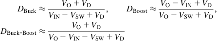
We realize it is becoming necessary to carefully understand the complete energy transfer process occurring in each of the three basic topologies, as shown in Figures 5.2–5.4. The process differs in each case. We now quickly glance through these figures, and see they include a hitherto unseen/unfamiliar form of the duty cycle equation, one that involves efficiency, η — initially an estimated or target efficiency, later we can use the actual measured one. Let us call these new equations “real-world” duty cycle equations. They are as follows:
![]()
We observe that these look remarkably similar to the very commonly used, first-estimate or “ideal” equations below:
![]()
The apparent similarity between the above two sets of equations is actually very deceptive. It belies their enormous differences. They could not be more different from each other. They literally represent the opposite ends of the spectrum ranging from ideal to real-world. Notice that we have consciously avoided using equality signs in the “ideal” (latter) set of equations above. The reason is, we want to be very clear that those are based on an assumption of zero losses. They are valid only for a converter with an efficiency of 100% (η=1), and of course we know nothing like that really exists in nature. On the other hand, the “real-world” set of equations (the former set above) are actually the most exact or accurate we can possibly encounter. Befittingly, we have used equality signs for them above (with some small reservations discussed later).
Just to refresh our memory from Chapter 1. The loss term can be written in terms of either input or output wattage as follows:
![]()
![]()
In either case, as η decreases, the loss increases.
Now, let us see what happens to the duty cycle in two specific cases.
(a) As we lower the input voltage, the duty cycle must always increase, because that creates a longer time for instantaneous input current to flow in from the source. In terms of average input current per cycle, the product VIN×IIN is thus maintained. Note that in the case of the Boost and the Buck-Boost however, since energy is delivered to the output only during the OFF-time, any increase in duty cycle leaves less time for energy to flow into the output. Therefore, to keep output power fixed, the instantaneous current must simultaneously increase as D increases (and that is why the center of ramp is IO/(1–D) for these two topologies, not just IO as for a Buck). However, so far we are assuming no change in efficiency (or output power).
(b) In the second situation, assume the input voltage is fixed but the efficiency decreases. The duty cycle must increase once again. Because that creates a longer time for additional current to be drawn in. In terms of average input current per cycle, the product VIN×IIN now increases, accounting for the increase in loss commensurate with the lowered efficiency.
The ideal equations are the most inaccurate, and lead to the smallest duty cycle possible for a given input/output condition. The real-world equations are the most accurate, and lead to the highest duty cycle (lowest efficiency) estimate. Between these two sets of equations, lie many other forms of duty cycle equations found in literature, all with varying degrees of accuracy. For example, we remember from Chapter 1 that by using the fundamental principle of voltseconds balance in steady state, we too came up with the following rather similar-looking duty cycle equations ourselves:
Notice that this time we are qualifying them by not using equality signs. Because we realize that though these equations explicitly include the drop across the diode and switch, and therefore factor in the conduction losses inside those two components, they continue to ignore several other smaller loss terms, like the (I2R) conduction loss in the DC resistance (DCR) of the inductor, or the various switching losses, or the AC resistance losses in the inductor, or the capacitor ESR losses, and so on — all of which if factored in somehow, will cause duty cycle to increase further. In the Appendix and in the solved examples in Chapter 19, we will see that the above equations have been extended to include the voltage drop across the DCR of the inductor. But the equality sign is still avoided, since we recognize that even those equations still leave out a whole bunch of other loss terms. Yet, admittedly, duty cycle equations with forward drops included as above, are certainly much better (more accurate) than the ideal equations presented earlier, and therefore a good starting point for most iterative calculations.
The final question remains: can we ever expect to provide an equation for duty cycle that is almost, if not perfectly, exact? For example, how do we really go about trying to model something like switching losses into a corresponding voltage drop (inside a duty cycle equation)? We really can’t go that route much further. But the good news is we can get very accurate equations, if we agree to club all the losses together and thereby rewrite out duty cycle in terms of overall efficiency η, and that leads us to the real-world duty cycle equations presented earlier. Admittedly, those equations do not reveal where the losses are occurring inside the converter, but they do make a very accurate statement linking efficiency to duty cycle. We therefore need them for the subsequent number crunching in this chapter.
But first, we do ask: why are they so accurate? And, which losses don’t they account for still? To answer these, we derive one of the above new equations as an example. Suppose we pick the Buck-Boost. The diode current of a Buck-Boost consists of a series of pulses of current with center of ramp IL and duty cycle 1–D. The average of that must equal the load current IO. Therefore,
![]()
or
![]()
On the input side, we have a series of switch current pulses with the same center of ramp IL and duty cycle D. The average of that must equal the input current. Therefore,
![]()
or
![]()
Equating the above two equations for IL, we get
![]()
![]()
But we also know that efficiency is by definition
![]()
So,
![]()
Equating the above two equations for IO/IIN, we get
![]()
which simplifies to
![]()
It is interesting that though power supply engineers are almost conditioned to assert “duty cycle in continuous conduction mode is independent of load current,” we actually relied on current to derive a so-called “current-independent” duty cycle equation above. So, is it really as current-independent as we had imagined? Quite clearly, no. But we also observe that the above derivation was somewhat surprisingly, not based on voltseconds balance in steady state, but on energy balance. Since energy is V×I, the derivation naturally included current.
Such subtleties aside, having derived the real-world duty cycle equations using energy principles, we can certainly go back and apply the results to our underlying voltseconds balance principle (which we recognize must always be true for any topology whichever way we look at it), and thereby create an ideal model of our real-world converter. That will make real-world converters much simpler to analyze, and very accurately so for most purposes. See Figure 5.1 where we have mapped our real-world converter circuit into an “equivalent” lossless (ideal) converter, by exploiting the remarkable similarity between the ideal and real-world duty cycle equations. The trick is to account for the real-world loss in two possible ways: either think of the input as having decreased from VIN to η×VIN in the corresponding ideal converter (implying that all losses occurred prior to the inductor), or imagine that the output has increased from VO to VO/η (implying that all losses occur after the inductor). The duty cycle is the same in both cases. And that follows from the fact that using simple arithmetic manipulation, we can write our real-world equation set above as follows:
![]()
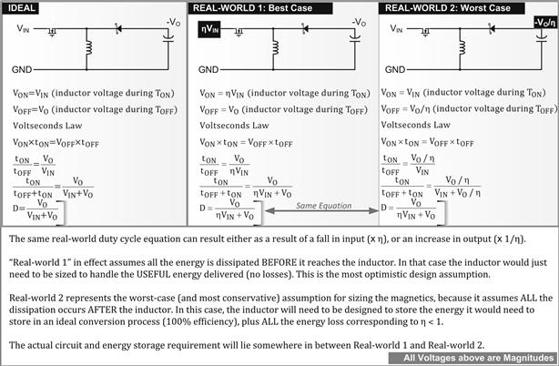
Figure 5.1: Creating equivalent ideal models for real-world converters and the effect on sizing of magnetics (example shown here is a Buck-Boost converter).
The two forms of real-world duty cycle equation seem equivalent, and in fact are — but only up to a point. Eventually, they lead to different ON-time/OFF-time voltseconds and therefore to magnetics of different sizes. The former interpretation (i.e., an effective decrease in VIN) leads to an optimistic (and possibly undersized) core, whereas the latter (an effective increase in VO) leads to a relatively larger core. In general, the latter model is a safer bet in design, especially if we don’t know where exactly the losses corresponding to the less than unity estimated/measured efficiency are occurring inside the converter. What really happens in a practical converter lies somewhere in between the two real-world models of Figure 5.1.
We have one last question: what losses are we (still) ignoring by writing out our duty cycle equations in terms of η? In other words: how exact are our “real-world” duty cycle equations above? If we understand the sample derivation above, we will realize that in effect we have ignored any current flowing in an equivalent resistance path parallel to the input and the output capacitors. We assumed that all the average current coming in from the input source went straight into the switch, and likewise, all the average current coming from the diode went straight into the load. In doing so, we implicitly ignored ESR-related and leakage losses in the input/output capacitors. Note that we can however estimate those losses upfront, and add/subtract them from what we call “PO” and “PIN” above, then the computations with the corrected values of input and output will be as accurate as can be. For example, if at the input we measure 10 V and 1 A, and estimate that we are losing 1 W in the input cap, we need to use PIN as 10–1=9 W. That is a VIN of 10 V and an IIN of 9 W/10 V=0.9 A. Similarly, if in the load we measure 5 V and 1.5 A, and we estimate we lose 0.5 W in the ESR of the output cap, we take PO as 7.5+0.5=8 W. That is a VO of 5 V and IO of 8 W/5 V=1.6 A. So, the converter efficiency is not 7.5 W/10 W=0.75, but actually 8 W/9 W=0.89. Though it must be pointed out we are still ignoring leakage current paths and related losses inside the switch and the diode. We are also ignoring any quiescent current losses in the PWM controller IC. We can correct for all of those losses upfront too if we want, but these losses are usually considered insignificant. With these qualifications in mind, the real-world duty cycle equations provided earlier (expressed in terms of η) are as accurate as can be; the ideal equations are as inaccurate as can be. The real-world duty cycle equations factor in switching losses, conduction losses (including DCR-related losses in the inductor) and even any AC resistance losses. They are therefore the equations we have relied upon in describing the concepts related to energy transfer in Figures 5.2–5.4.
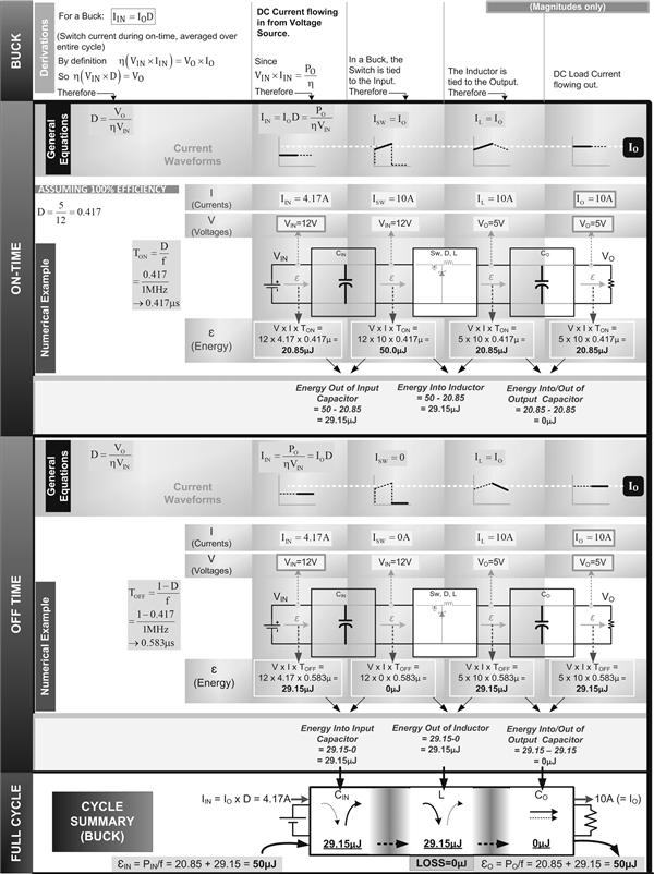
Figure 5.2: The Buck topology energy transfer chart and a 50 W converter example.
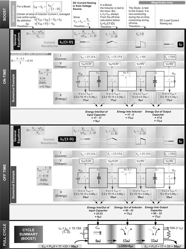
Figure 5.3: The Boost topology energy transfer chart and a 50 W converter example.
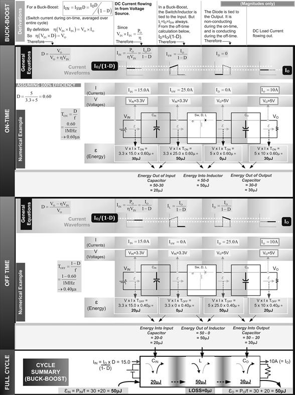
Figure 5.4: The Buck-Boost topology energy transfer chart and a 50 W converter example.
The Energy Transfer Charts
We now look at Figures 5.2–5.4. Here, we present each topology in turn, showing each step of their internal energy transfer process. To focus on energy and storage function, observe how we have split each topology into three reactive (energy storage) blocks — the input capacitor, the inductor (with switch and diode attached to switch its connections around), and the output capacitor.
In each topology chart, we first look at what happens during the ON-time. We figure out V and I at each point of the circuit. Note that the equations for current used here are all very accurate, since they are based on the accurate (real-world) equations for D. We multiply V, I and the corresponding time interval (V×I×time) to get the corresponding energy. Then from the energy difference on either side of any given reactive block, we can calculate how much energy is either getting in (i.e., stored), or coming out (i.e., extracted) from any particular block. We then repeat the same process for the OFF-time. Finally, we compile the “energy balance sheet”: here we compare the energy in/out numbers of the OFF-time with the energy in/out numbers for the ON-time. We realize that in every case, if we store a certain amount of energy “X Joules” in any given block during the ON-time, then during the OFF-time, exactly that amount of energy, X Joules, must be extracted. And likewise, if we extract a certain amount of energy X Joules during the ON-time, exactly that very amount of energy must get stored during the OFF-time, and so on. Because, this is a steady state by definition — from one end of the converter to the other. We can confirm from the figures that, indeed, there is no incremental buildup, or decrease in energy, after one complete cycle in any of the three reactive elements, the inductor or the input and output capacitors. Yes, if we had not got this result, we should have been very worried. It would have indicated to us that either our topology was somehow flawed, or more likely, the equations we had used to calculate the energy terms (and the corresponding currents and duty cycle) were not very accurate. We do note though, that in the sample numerical examples presented in Figures 5.2–5.4, we have still assumed 100% efficiency. That has been done only for simplicity at this early conceptual stage; later, we will repeat the same process for a real-world case (η<1), and see how the picture changes. Note also that the numerical examples within these figures all use 50 W converters of each topology, just for comparison sake.
We can learn several things from Figures 5.2–5.4. We list some of them here.
(a) A Buck-Boost inductor has to handle all the energy coming toward it — 50 μJ as per Figure 5.4, corresponding to 50 W at a switching frequency of 1 MHz.
Note: To be more precise for the general case of η≤1: the power converter has to handle PIN/f if we use the conservative model in Figure 5.1, but only PO/f if we use the optimistic model.
In contrast, the inductors of the other 50 W converters shown in Figures 5.2 and 5.3 have to handle only a fraction of the energy flowing between input and output. But exactly what fraction is that?
(b) To answer the above question, we can derive closed-form equations relating to inductor energy storage, based on these three energy transfer charts. We have done that in Figure 5.5, from which we get the following energy packet sizes for each topology:
![]()
![]()
![]()
This shows us what fraction of the energy we were talking about above. Note that these derivations were based on the conservative real-world model, that is, where we factor in efficiency, by thinking of the output as having increased to VO/η rather than the input decreasing to VIN×η.
We thus realize that the Buck and Boost inductor storage requirements are based not only on input/output power, but also on input and output voltages (D). The Buck-Boost energy requirement is based on power alone — the fraction of power that it has to handle is 100% (i.e., all of it).
(c) We know that in all topologies, low input voltage corresponds to high duty cycle and high input to low duty cycle. So, we can conclude that for a Buck, Δε (the energy packet going in/out of the inductor every cycle) is at its maximum when 1–D is highest, i.e. where D is lowest, that is, when the input voltage is at its highest level. This is consistent with what we learned in Chapter 2 regarding “worst-case input” for the Buck. For example, if we have a Buck delivering 3.3 V output, for an input range of 5–15 V, we need to design its inductor (pick the core volume) at the worst-case input of 15 V.
(d) Similarly, we recognize that for a Boost, Δε (the energy in/out of the inductor every cycle) is at its maximum when D is highest, that is, when input is at its lowest level. This too is consistent with what we learned in Chapter 2 regarding “worst-case input” for the Boost. For example, if we have a Boost delivering 24 V output, for an input range of 5–12 V, we would design its inductor at the worst-case input of 5 V.
(e) Coming to the Buck-Boost, we had asserted in Chapter 2 that we need to design its inductor at the lowest voltage of the input range. In the next section, we will see why that is true, though not very obvious so far. We are confused because we have just calculated that the energy that gets cycled through the inductor of a Buck-Boost is fixed — Δε=PIN/f irrespective of the input voltage. And that being undeniably true, we can rightly conclude that a 50 W “universal input” flyback, for example (typical input range being 85–265VAC), does not need to have a bigger transformer than a 50 W flyback designed only for Europe (typical input range being 195–265VAC).
Note: We must keep in mind that the above statement applies only to a flyback/Buck-Boost. A Boost PFC stage designed only for Europe will have a much smaller inductor than a Universal Input Boost PFC.
At the same time it is equally accurate to maintain that we really should design the inductor of a flyback/Buck-Boost at the lowest input voltage of its input range. In the next section, we will learn why both statements above, seemingly contradictory, are in fact simultaneously true.

Figure 5.5: The closed-form equations governing inductor energy storage requirements in the three topologies.
Peak Energy Storage Requirements
So far, our focus has been on calculating the amount of energy going in and out of the inductor per cycle in the three topologies. In doing so, in effect, we ignored the crest factor (peak to average ratio) of the current waveforms. And that means we ignored the effect of the current ripple ratio r. Looking at Figures 5.2–5.4 once again, we realize that we had based all our calculations on the center of the current ramp IL, and it was on that basis we had calculated the energy swing (packet) Δε. However, in reality, on a real-time basis, the current ramps up and down every cycle. Therefore, there is a certain peak energy εPEAK associated with the peak current. We must ensure not only that the inductor can store a certain amount of energy every cycle, but that it can handle the instantaneous energy at any given part of the cycle, without saturating.
We can easily calculate the relationship between Δε and εPEAK as shown in Figure 5.6. The key important relationship is this
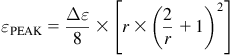
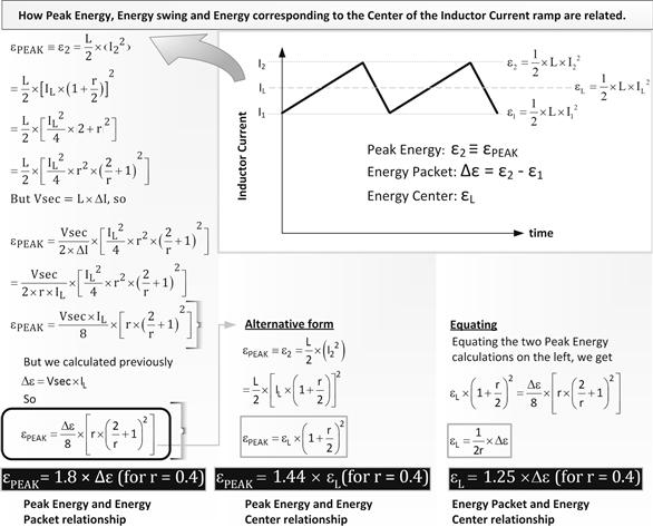
Figure 5.6: Relating the energy swing to peak energy (and other useful energy relationships).
This equation applies to all topologies. The term Δε in it however depends on the specific topology. So, for a typical value of r=0.4 (ripple of ±20%), we get a peak value exactly 80% greater than the energy swing (a default factor of 1.8). In other words, in Figure 5.4, for example, the inductor energy swing for a Buck-Boost was 50 μJ, and we now realize that to store this, with an inductance selected to give us an r of 0.4, we actually need an inductor sized such that it can handle not 50 μJ, but the peak of 50×1.8=90 μJ (instantaneously). Basically, the inductor is constantly moving between the extremes of 40 μJ and 90 μJ, with a delta of 50 μJ. Similarly, in Figure 5.3, we need to pick a Boost inductor sized to store 17×1.8=30.6 μJ instantaneously.
Note: In power supplies, while calculating current stresses (as we will do in Chapter 7), something called the “flat-top approximation” is often used. In this approximation, we basically ignore the AC (swinging) part of any current waveform and approximate the trapezoidal current waveform with a rectangular one (extending to the center of ramp, i.e., the average inductor current). This is also called the “large inductance approximation,” and corresponds to setting r=0. This approximation typically gives surprisingly accurate results for the RMS value of the switch current (within ±10% for r less than 0.5 and any duty cycle from 10% to 90%), but not for capacitor currents. In our present case, we ask: what does the flat-top approximation do to the selection of inductors? Is it fairly accurate? Quite the contrary as we see below.
We now ask the seemingly obvious: why not reduce the current ripple ratio r further (i.e., increase L)? We intuitively feel that would lower the peak value of current and possibly the peak energy, and therefore the size of the inductor. We intuitively feel that would bring the peak value close to the value at the center of ramp. So presumably it would lead to a smaller core size (with lesser required peak energy handling capability).
But that is completely wrong. The correct answer, and one of the most counterintuitive ones in magnetics design, is that in reality, the smallest core size is obtained by raising r (lowering the inductance, not raising it). Yes that increases the peak currents, worsens the crest factor. But somehow it helps reduce inductor size (and energy too)! Mathematically it is simple to explain. The “culprit” is the odd term involving current ripple ratio r in the εPEAK equation above. We isolate that term below.
![]()
where
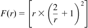
If r is very small, 2/r is >>1. So,
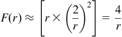
We see that the F(r) function imparts an approximate inverse proportionality (y=1/x) shape to all the peak energy curves, as we can confirm when we plot them out using Mathcad in Figure 5.7. All the curves have the same shape, and in fact are the very same normalized curve we had plotted in Figure 2.6 earlier. This basic shape shown remains unchanged for all topologies and all duty cycles (i.e., all input/output voltages), and even all switching frequencies. It is thus fundamental, and is perhaps the most important curve we can study for improving our overall understanding of switching power supplies. It also highlights the tremendous simplicity that results if we start to view magnetics in terms of current ripple ratio r rather than L. Because, as we can see, all the curves have a knee at r≈0.4. They do not show that property if we look only at L.
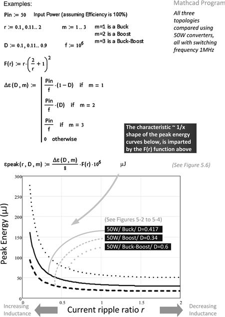
Figure 5.7: Peak energy curves, core size, and optimal inductance (current ripple ratio).
Realizing that the vertical axis in Figure 5.7 is effectively just the size of the core, we conclude that size of core decreases as L decreases. That also incidentally explains why we often say “reduce the inductance” when we really mean “reduce the inductor,” and get away with it each time.
The question remains: how can we not mathematically, but intuitively, explain this seeming paradox — that is, why the energy handling requirement decreases if we reduce L, instead of increasing. The answer to this is that when we increase L and thereby reduce the peak value of current, we have to increase L by a comparatively much bigger factor to achieve a certain, relatively small, reduction in peak current. So, energy, which depends on both L and I through the equation ε=(1/2)×LI2, actually increases as we increase L. That is why the correct direction toward achieving core size reduction is by decreasing L (i.e., raising r), not increasing L (lowering r). The paradox is resolved. The flat-top approximation should never be used for magnetics design or for capacitor design.
We can now ask: if that is so, why not decrease L even more, to achieve the minimum possible core size? Yes indeed, we can do that. But there are penalties as was made obvious in Figure 2.6. However, despite that penalty, it is not uncommon in low-power applications to find low-cost DC–DC or AC–DC converters operating in critical conduction mode always (i.e., r=2, exactly between CCM and DCM). We will find their inductors are really much smaller than CCM converters of the same output power. But along with high r, we will also likely see on the board some rather low-RDS MOSFETs (perhaps in large packages), and low-ESR capacitors (or many capacitors in parallel) — an obvious effort to combat the adverse effects of the rather high peak and RMS currents as indicated in Figure 2.6. That is the “penalty” we may decide to pay for using smaller inductors.
Since the peak energy curves always have a knee at around r≈0.4, the most optimal value in almost all applications is r≈0.4 — that becomes an almost universal design target of sorts, irrespective of the topology, application conditions, and switching frequency. This is equivalent to±20% ripple. Note that we could never have managed to declare a certain, fixed “optimum inductance value” for every single switching converter on earth. But certainly, talking in terms of r, we have come pretty close to doing just that. Finally, once we have fixed r, we can calculate L based on that assumption. As expected, the equations connecting r to L (see reference table in Appendix), do depend on topology, application conditions and switching frequency. That is where all the dependencies enter the picture.
One question remains. Previously we had stated that a flyback transformer for, say, a 50 W application designed for Europe alone, would have the same size as one designed for the entire world, including the US (disregarding any differences in efficiency here). This was because we had discovered that the amount of energy the transformer has to cycle back and forth per cycle equals PO/f, and that has nothing to do with the input voltage. So, why do we still insist we need to design the Buck-Boost at its lowest input voltage? The answer is right above us actually. It is the crest factor that is responsible. As we lower the input, the peak current and energy increases. So, to be sure we avoid saturation, we need to design the transformer at the lowest input voltage (max D) of our expected input range. That is always true for a Buck-Boost/flyback. However, when we compare a European flyback transformer designed for r=0.4 at 195VAC, with a North American flyback transformer designed for r=0.4 at 85VAC, there would be no difference because the numerical value of the term F(r) is the same in both cases. The crest factors are identical and so εPEAK is the same in both cases, and so is the required transformer size (see also Figure 14.4).
Calculating Inductance Based on Desired Current Ripple
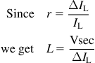
Having understood how easy it is to start with a general design target of r=0.4 (in most cases), for all topologies, applications, and frequencies, we now want to connect L and r. In particular, we want to derive the relevant equations presented in the Appendix, and also re-examine the “L×I” rule which was presented earlier in Figure 2.12. Note that here, for easy reference and representation, we prefer calling Voltseconds as “Vsec” here, rather than as “Et” as in other chapters, but the two are the same. In Figure 5.8, we have derived the L versus r equations for each topology. We have also then shown that the “L×I rule” is universal. It applies to all topologies and can be written as
![]()
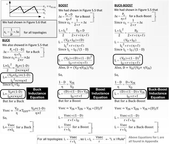
Figure 5.8: Deriving L versus r relationships and the universal “L×I rule.”
We now show that this is just the inductor rule V=L dI/dt in a more exotic form.
In other words,
![]()
Solving for V (applied voltage across inductor during ON or OFF time)
![]()
We thus get back our well-known inductor equation. They are the same equation!
In Figure 5.9, we have also calculated the DC transfer function VO/VIN for all topologies. And from that, we re-derive the equations for inductance, this time starting with the L×I rule. We have ultimately re-cast the inductor equations in terms of μH and MHz for greater ease of use. See Chapter 19 for some relevant solved examples.
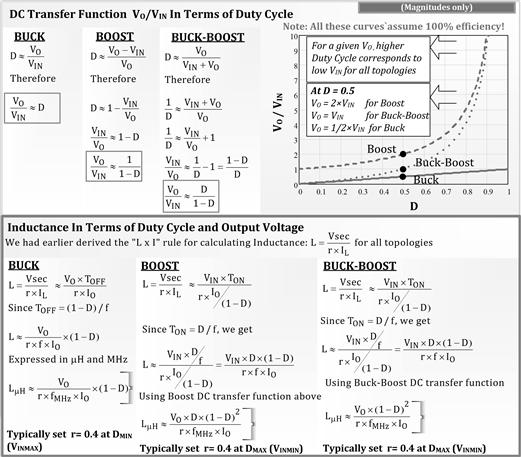
Figure 5.9: DC transfer function and inductance design equations starting from the “L×I rule.”
Part 2: Energy to Core Sizes
Magnetic Circuits and the Effective Length of Gapped Cores
With energy transfer and storage concepts understood, we can start discovering how they point to the optimum core size in any given application. But to do so more effectively, we need to add to, and refine, some of the magnetic concepts presented in Chapters 2 and 3.
Let us start by looking at Figure 5.10. This is a “magnetic circuit” — the electrical equivalent of a magnetic component. We can see how reluctance in magnetics plays a part analogous to resistance in electrical circuits. Flux, defined as ϕ=B×A (for uniform fields), plays the role of current. The term N×I (Ampere-turns), called magnetomotive force, is analogous to voltage source in electrical circuits.
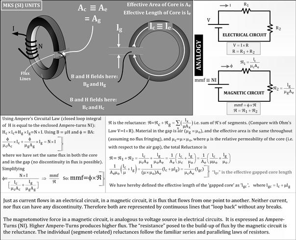
Figure 5.10: Magnetic circuits and effective length of gapped cores.
If we have an ungapped core, its effective length is basically the perimeter of an imaginary circle drawn through the center of the core. That is called “le” or effective length. The effective area, “Ae,” is almost exactly equal to the geometrical cross-sectional area of the core. The reluctance is le/μcAe, where μc is the permeability of the core material (using MKS units). However, when the core is gapped, we see that the reluctance increases to lgc/μcAe, where lgc=le+μlg, and lg is the length of the gap. In effect, lgc is behaving as the new effective length of the gapped core. In other words, as soon as we introduce an air gap, the effective length that appears in the magnetic circuit is not just le but le+μlg, where μ is the relative permeability of the core material. Relative permeability is the permeability relative to air, that is, μ=μc/μo. It seems that for all practical purposes, the air gap lg has gotten multiplied by the relative permeability of the surrounding material μ, and then added to the effective length le of the core (without gap) and that has become the new effective length of the gapped core. For example, if we were using ferrite (typical relative permeability of 2,000), and the air gap was a mere 1 mm, this tiny gap actually plays the part of an effective length of core material equal to 2,000×1=2,000 mm, or 200 cm. That is the reason reluctance changed as follows:
![]()
The good news is that the “200 cm” (magnetic length) extra magnetic length only occupies 1 mm (physically). Also, eventually, the adder μlg becomes much larger than le, and so le is often ignored in comparison.
But what use is this extra length? Well, for one, the effective gapped volume goes up from Ae×le to Ae×lgc. Intuitively that means we have a much larger core volume (magnetically) than we thought we had (geometrically). The air gap has in effect become a “core volume multiplier” of sorts. And further, provided we can create strong-enough fields, we expect to be able to store much more energy too. We have a much “bigger box”.
However, the simplest and most elegant way to quantify all this and discuss it mathematically-plus-intuitively is by focusing not on the adder term (μlg), but on the ratio (le+μlg)/le (the new effective length, after gapping, divided by the old effective length, before gapping). If we do that, the equations of gapped cores become extremely simple to handle. That factor is called the “z-factor” (or “gap factor”).
![]()
We see that the net reluctance increases from le/μcAe for an ungapped core to zle/μcAe for a gapped core. So, “z” is the reluctance multiplier term.
Stored Energy in Gapped Cores and the z-Factor
Now we start to look closely at the magnetic fields, because that is where magnetic energy is ultimately stored. The effect of the air gap can be seen clearly from Figures 5.11 and 5.12. As expected, since the air gap has caused the reluctance to increase, the B-field drops from μcNI/le in an ungapped core, to μcNI/zle in a gapped core (think in terms of the electrical circuit analogy in Figure 5.10). But wait: where exactly is this reduced B-field we are referring to — are we talking about the B-field in the core or in the gap? B is related to flux through B=ϕ/A, and since flux is continuous across boundaries, so is B. The B-field inside the core and in the air gap is the same. We need to remember that B (its normal component) is continuous across material boundaries. So, the B-field is μcNI/zle, both in the core and in the gap, as indicated in the figures.
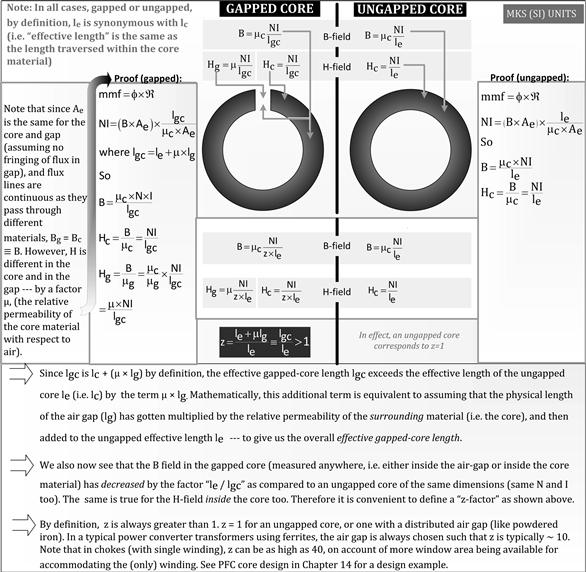
Figure 5.11: Comparing the B and H fields in gapped and ungapped cores.
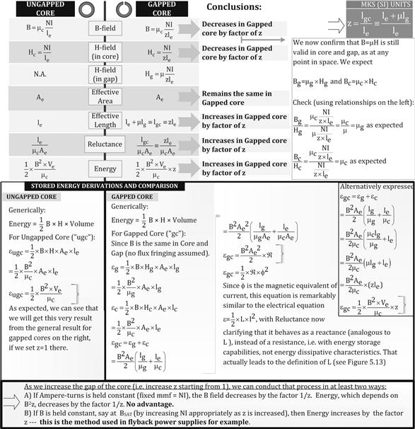
Figure 5.12: How gapped cores store more energy.
However, the H-field has different values in the core and in the gap. We remember that by definition, Hc=Bc/μc and Hg=Bg/μg. The H-field at any point in space is: the B-field at that point, divided by the permeability at that point. Since Bg=B, and the permeability of air (μg≡μo), is different from the permeability of the core (μc≡μμo), the H-field in the core and in the gap are different. We see that, because of the increased reluctance (due to the air gap), the H-field does in fact drop from its value of NI/le in an ungapped core, to NI/zle in a gapped core. But note that this reduction occurs only inside the core.
We ask: does the reduction in the H-field (within the core material) significantly reduce the overall energy storage capability? Yes, it does reduce the energy stored in the core material, but the energy in the air gap more than makes up for it. Fields aside, just in terms of volume, in a typical gapped core, the volume of the core material is Ae×le. That is typically a small part of the total effective volume of the overall gapped structure, Ae×lgc. The bottom-line is that what happens to the B and H fields inside the core material is hardly important in a gapped core. The effects of the air gap predominate. Though, we must keep in mind that the gap wouldn’t exist, were it not for the presence of the core around it.
In gapped ferrite transformers, a typical target value for z is 10. So, we realize that the H-field in the core typically drops by a factor of 10 compared to the value it would have had in an ungapped core. However, the H-field in the gap increases dramatically. For a ferrite transformer for example, with a μ (relative permeability) of around 2,000, the H-field in the gap is about 2,000/10=200 times the H-field of an ungapped core. The density of the stored energy (i.e., energy stored per unit volume) at any given point in space is by definition (1/2)×B×H, where B and H are the magnetic fields at that point. This increase in H inside the air gap, combined by the fact that the effective volume of the air gap is now μlgAe not just lgAe, helps in substantially increasing the energy storage capabilities of gapped cores. This is described more clearly in Figure 5.12.
Note: The effective length of the magnetic structure without any air gap is le. (The reluctance is le/μμO.) With air gap added, the total effective length becomes le+μlg. (The reluctance is (le+μlg)/μμO or zle/μμO.) In effect, the air gap has added a magnetic length equal to μlg, instead of just lg. Therefore, the increase in the total effective volume due to the presence of the air gap is Ae×μlg.
In Figure 5.12, we have summarized and tabulated the key changes that occur when we gap a core. Of particular importance is the fact that the energy in the entire structure of a gapped core (core+gap) is z times the energy of an ungapped core, for the same B-field. In other words, we need to increase the Ampere-turns (the mmf) to compensate for the increased reluctance due to gapping and thereby maintain B at the same value as in the ungapped core. We also realize that philosophically, we always want to use whatever resources we have, to the maximum extent we can. That limit, in this case, occurs when we operate the core close to its saturation flux density (BSAT). For ferrites BSAT is typically 0.3 T, or 300 mT, that is, 3,000 G in CGS units. Therefore, we may want to compare the energy storage capability of, say, an ungapped EE42 core operating at 300 mT, with a gapped EE42 core operating at 300 mT. We will then find that the ratio of their energy storage capabilities is equal to z. That highlights the importance (and simplicity) of looking at things from the viewpoint of the z-factor.
How do we maintain the same B-field as we introduce an air gap? Well, since B is proportional to NI/z, if z increases as we increase the gap, we need to increase the product NI by the same factor. However, we now realize that, typically, in switching converters, the currents are all pre-determined — they depend on load current and duty cycle. In other words, we have no control over current. So, in such a case, we will need to increase the number of turns (by the same factor). And that is what ultimately bounds the maximum practical value of z — because eventually we need to be able to accommodate all these additional turns on the core. For most commercial E-type cores, the window area available is commensurate with a z of up to 40 if we are designing a simple choke (i.e., an inductor with a single winding). But for flyback transformers for example, a lower value, z=10, is a more practical value for the air gap, and for picking an optimal E-core in most applications.
Finally, in Figure 5.13, we connect to inductance and show that
![]()

Figure 5.13: Deriving the equations for inductance.
Always keep in mind that we are using MKS units all through this discussion unless otherwise stated. So, Ae is in m2, le is in m, and so on.
Note: We can now understand why in a switching power supply transformer, a z of 10 is a good target, whereas in a choke, a z of 40 is acceptable. As we start changing the number of turns with an intent to keep B fixed as we increase the gap, we need to apply another constraint — remember that we have a target inductance too, which we need to fix. Since we have just learned that L is proportional to N2/z, for a constant L, z must be proportional to N2. Since the maximum possible number of (Primary) turns in a transformer is half the number of turns we can put on a corresponding choke, the corresponding z is 1/4th. Therefore, if a good target for a choke is z=40, then for a transformer it is z=10. We will use the z=40 condition when designing a PFC choke later in Chapter 14. We will use z=10 as an example later in this chapter.
Note: In this entire core volume selection process, we are only talking in terms of energy storage capability. Which is why we are considering a flyback transformer, not a Forward converter transformer for example. In the latter case, the core really does not store any significant amount of energy, because the Primary and Secondary winding conduct simultaneously, and so useful energy is transferred directly through the transformer during the ON-time itself. The only stored energy component in the transformer core is the small excitation (magnetization) energy, which is subsequently recovered through a thin energy recovery winding during the OFF-time. In a Forward converter, the output choke is the energy storage component. But it is usually a toroid with a distributed air gap (e.g., powdered iron). That is a case of z=1, and we should just use the stated permeability and maximum number of turns, as provided by its vendor.
Energy of a Gapped Core in Terms of the Volume of the Core
In Figures 5.14 and 5.15, we derive the final, general, closed-form energy-density equations for gapped cores, using any general magnetic material, keeping in mind the specific demands of the topology on hand. In the two figures, we have alternate (but equivalent) forms and derivations of the following key equations:
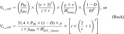
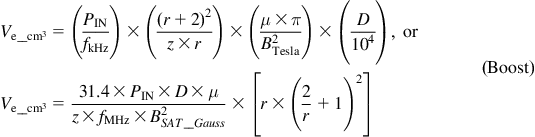
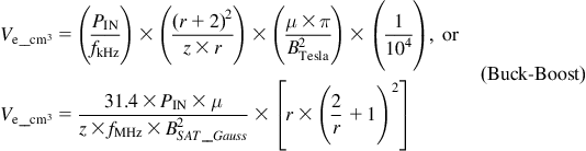

Figure 5.14: Useful equations for core selection for each topology.
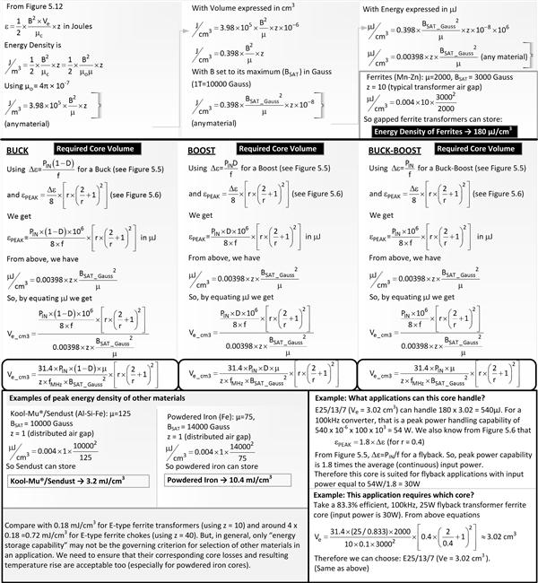
Figure 5.15: Useful equations for core selection and numerical examples.
As we expect from our understanding of energy transfer principles vis-à-vis the three topologies, the Buck and Boost equations above depend on D, and therefore on the specific input and output voltages of the application. However, the Buck-Boost demands the highest core volume, and that is independent of D as we expected.
We also see that if z is set to around 10 as suggested for ferrite transformers, then the core volume can be reduced 10 times since in all cases above, Ve is inversely proportional to z. And we realize that was the purpose of the air gap to start with. We should also keep in mind that for chokes, as opposed to transformers, a z of around 40 is usually achievable within the available window area of E-type cores.
The alternative derivation of core volume in Figure 5.15 is based on the following approach: (a) first calculate the energy packet size for a given application, (b) connect that energy packet size to the peak energy, and then (c) look for a core that can handle that peak energy. With that approach, the question, independent of topology, is: how much energy can a given core handle? We can express this energy density as μJ/cm3, or J/m3, and so on. Some useful equations for it are provided in the figure. Note that some numerical examples showing how to select cores are provided within Figure 5.15 too, in particular for a flyback. Note also that if we are using powdered metal cores, the core and copper losses are more likely to be the limiting factor and will thus determine core size, not the energy density capability of the material. So, we may need to use the core volume selection equations with caution. However, for ferrite, gapped (z>1) or ungapped (z=1), they are a good reference for picking the right cores.
Part 3: Toroids to E-Cores
In previous sections we derived energy equations based on toroids, and then implicitly extended them to E-type cores when talking of the required core volume. That is quite acceptable for determining volume, but things can get confusing when we try to actually implement a certain calculated air gap in particular. For example, suppose we calculate the air gap as 0.1 mm. We know that this calculation in effect assumes a toroid. So, how do we implement “0.1 mm” in a triple-limbed E-type core? To answer that we have to understand E-type cores better. For one, we keep in mind that all the terms: effective length, effective area, and effective volume, were originally defined with reference to a toroid, as per the magnetic circuit in Figure 5.10. So, we need to figure out what these quantities are with reference to the specific geometry and dimensions of cores like EE cores, ETD cores and EFD cores (generically referred to as E-type cores). In other words, we need to map such cores into an equivalent toroid. The way to mentally visualize this is shown in Figure 5.16.
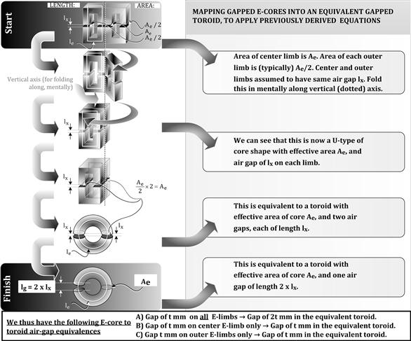
Figure 5.16: Mapping an E-core into an equivalent toroid.
We can visualize that in an E-core, by continuity of flux lines and symmetry, the flux ϕ going through the center limb divides up equally into the two outer limbs. Since B=ϕ/A, if ϕ/2 is in each outer limb, to keep the B-field the same throughout the core, the area of the outer limb needs to be half the area of the center limb. And that is how E-cores are essentially designed — with the area of each of the two outer limbs equal to half the area of the center limb — because no one typically expects, needs, or wants, the outer limbs saturating before the center limb, or the other way around (we want same B throughput). If they saturate differently, that would only represent wasted core material in most applications.
Further, the cross-sectional area of the center limb is almost exactly equal to the effective area, Ae, of the core’s equivalent toroid (as stated in the datasheet). The area of the outer limbs of the E-core must therefore be almost exactly half the effective area. This is shown in Figure 5.16.
We also realize that to set a calculated air gap of say 0.1 mm (with reference to an equivalent toroid), we can simply set an air gap of 0.1 mm in the center limb. We could achieve the same by grinding 0.05 mm off each center limb half, or 0.1 mm off only one half. There would be no gaps on the outer limbs; the outer halves would lie flush against each other. Alternatively, we can just take regular E-core halves (with no center or outer limb grinding), and put 0.05 mm polyester spacers on the two outer limbs. That would create a gap of 0.05 mm in all three limbs. This is illustrated in Figure 5.17, using an air gap of 0.26 mm as an example.
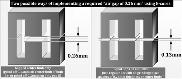
Figure 5.17: Two ways of setting an air gap of 0.26 mm.
One of the subtle advantages of using an air gap is that air starts dominating the reluctance, and ultimately the entire characteristics of the gapped structure. We had indicated this previously too.
![]()
This is the same as saying
![]()
It is well-known that ferrite manufacture is a very complicated process, and has rather wide tolerances inherently. For example, toward the end of the process there is a stage called sintering, in which significant, and not completely predictable, volume shrinkage occurs. So the manufacturer has to guess the amount of shrinkage that will occur, and start with a higher volume. So, the final mechanical tolerances are not very good. Nor the other characteristics. However, by introducing an air gap, we can swamp out these variations to a great extent and make it all more dependent on the characteristics of the air gap. That helps make the behavior of the overall gapped structure much more predictable and repeatable. That is why even in Forward converters, a small air gap (~0.1 mm to 0.2 mm) is often deliberately introduced in the transformer, even though we realize that energy storage is not the purpose of the transformer of a Forward converter, unlike that of a flyback. Of course we are left with higher energy to recover and circulate through the energy recovery winding, but the increased reliability is usually considered worth it.
Finally, in Figure 5.18, we show how to connect the geometry of an E-core to its effective (published) length, area, and volume. That finally completes our deep dive into E-cores.
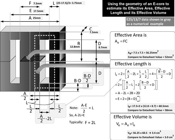
Figure 5.18: Calculating effective length, volume, and area from core geometry.
Part 4: More on AC–DC Flyback Transformer Design
Now we will apply what we have learned to an AC–DC transformer and design it down to the wire, literally. The first thing to keep in mind is that the process is iterative. For example, in the lowermost example in Figure 5.15, we coincidentally “found” a core with exactly the same volume as our requirement. But if, for example, the efficiency was somewhat lower, we would have required a larger volume. We would then “just miss out” on using the E25/13/7. That would be sad because the next available core size may be rather too large, and would represent overdesign. At this point we could compromise a little on our target current ripple ratio and select say r=0.55 instead of 0.4. The required core size would then reduce and the E25/13/7 may be in the ballpark once again. Yes, there would be some impact on the input and output capacitors, in particular in terms of their higher RMS current and heating, but there would be much less impact on the switch dissipation and almost no effect on the diode ratings or its dissipation. We would need to set higher peak current limits and so on. Another possible direction is to increase the air gap just a little (without changing the inductance or r). That would demand a few more turns. But if these turns can be physically accommodated in the available window area, and if we are also willing to accept the slightly higher copper losses, that could be a good way to go too. Eventually, we can evaluate all the side-effects, and better optimize our converter design.
In Figure 5.19, we start by providing perhaps the easiest equation possible for picking a ferrite flyback transformer
![]()

Figure 5.19: AC–DC flyback design example (part 1).
Its simplicity belies the fact that it is actually an exact equation, but based on certain defaults applied to the general equation derived previously. We have picked z=10 (this corresponds to a typical air gap in ferrite transformers), r=0.4 (this is the optimum target current ripple ratio and indirectly determines the inductance L), BSAT=3,000 G and μ=2,000 (i.e., ferrite assumed).
Going back to Chapter 3, we had presented the following, slightly more general, equation in the subsection titled “Selecting the Core”
![]()
Since 0.7×[(2+0.4)2/0.4]=10.0, we can see this was exactly the same equation we have presented directly above (and derived), with the difference that we have now set r to a default value of 0.4 too.
In Figure 5.19, we see that by very simple steps based on previous derivations, we now arrive at the same (~3 cm3) volume determined in the previous example in Figure 5.15, and we again select the same core, that is, E25/13/7.
Note that the numerical examples in Figure 5.19 apply to a 30 W input. That can refer to an ideal 30 W output converter (with 100% efficiency). It also applies to a real-world converter with, say, 25 W output power and 83.3% efficiency, because 25/0.833=30 W. In Example 2 of the same figure we apply the concepts to an AC–DC flyback. We have chosen an 83.3% efficient 25 W Universal Input flyback with an output of 5 V at 5 A. Here we invoke the concept of reflected output voltage, VOR, as discussed in Chapter 3, in particular in Figure 3.2.
Note that in Figure 5.19 we discuss a “Best-Case Estimate” and a “Worst-Case Estimate.” We now see more clearly what we meant in Figure 5.1. Obviously, “Best-Case” corresponds to “Real-World 1” and “Worst-Case” to “Real-World 2.” We see how the answer to the question “where do the losses occur inside the converter — before or after the inductor?” affects the size of the core (peak energy), the voltseconds and the calculated inductance. Conservatively speaking, we can design the core/transformer as per the assumption that all the losses occur on the secondary side of the transformer. That is the worst-case estimate. But if we know better, we can do a more accurate estimate of peak energy requirements.
Note: In Figure 5.19, we have used a rectified voltage of 127VDC for simplicity. That will certainly be valid for a flyback with a very large input capacitor. But we must remember the input capacitor peak-charges when the input bridge conducts and discharges during the rest of the AC half-cycle. Therefore the voltage at the input of the flyback undulates at twice the AC line frequency (100 Hz or 120 Hz) between two voltage levels that are typically quite far apart. So in fact, an “average” value between the two levels should be rightly taken as the effective DC input voltage to the flyback. But that is a very involved calculation which depends on the value of the input capacitance and so on. We will take that up in Chapter 14. For now we stick to 127VDC as the input.
As indicated in Figure 3.2, in the Primary-side equivalent model, the output voltage is VOR. Since in Figure 5.19, we have chosen a VOR of 100 V, a 25 W converter is, on its Primary side, equivalent to a Buck-Boost with an input of 127 V and an output of 100 V at 0.25 A. Note that the efficiency is not 100%. And that gives us an opportunity to “close the loop” in our unique journey, one that started with the energy transfer chart in Figure 5.4. In that chart, we had, for simplicity sake, taken a numerical example with 100% efficiency. But we had insisted we had taken exact equations, and had said they were valid even if the efficiency was not 100%. Now we can prove it. In Figure 5.20, we repeat the previous energy transfer calculations, but this time for the non-ideal case of Example 2 of Figure 5.19.
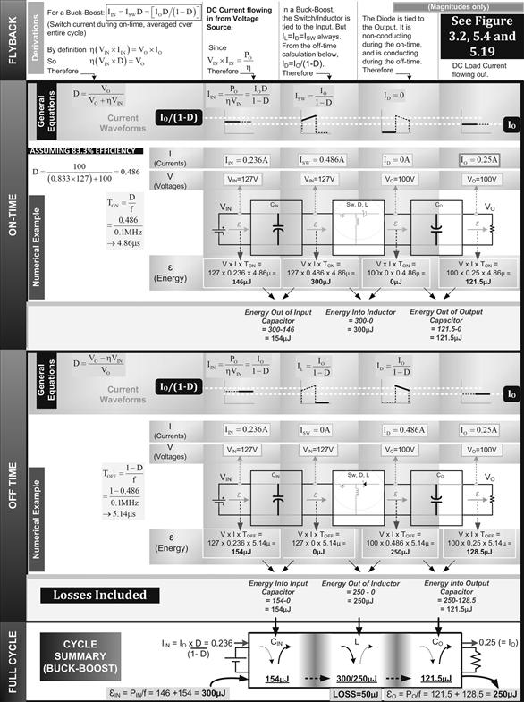
Figure 5.20: Energy transfer chart for a flyback, losses included.
Here are the results. We see that 250 μJ comes out per cycle. At 100 kHz (0.1 MHz), that is equivalent to a power output PO of 250 μJ×105=25 W. On the input side, we have 300 μJ coming in per cycle, corresponding to PIN=30 W. We can also now clearly see that exactly 50 μJ (corresponding to 5 W) is lost somewhere in the middle block. The energy balance sheet is already complete, vindicating all our previous equations and treatment. The final numbers add up in Figure 5.19 just as they did in Figure 5.4.
Note: The center block consists of the inductor, switch, and diode. The 5 W dissipation occurs somewhere inside this block—say, as conduction losses, or switching losses, or DCR losses, or AC resistance losses, and so on—almost anything that can take place inside this block that is directly related to the actual power conversion process (no leakage losses considered here). The energy chart is not intended to make any statement on exactly where the losses occur within this center block, and whether they can be considered before or after the inductor. The purpose of the energy transfer charts was only to clarify the concepts relating to energy storage and topology dependency.
In brief, provided we use the right form of duty cycle (i.e., using η), then all the equations we have presented and used for the current at different parts of the circuit are also valid, irrespective of efficiency, frequency, wattage, and so on. The implicit assumption however, right from the beginning of this chapter, is that we are operating in continuous conduction mode (CCM).
To select wire gauge correctly, we present a primer in Figure 5.21. This has several useful relationships to figure out: skin depth, diameter, AWG and current-carrying capability. Finally, we continue the AC–DC flyback example we started in Figure 5.19, in Figures 5.22 and 5.23. By the end of that, we know the entire procedure for designing a flyback transformer.
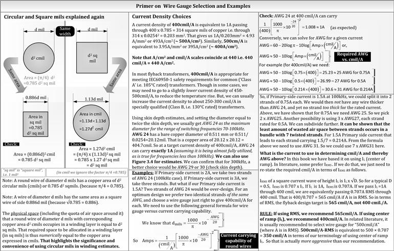
Figure 5.21: Primer on wire gauge selection for flyback and other topologies.
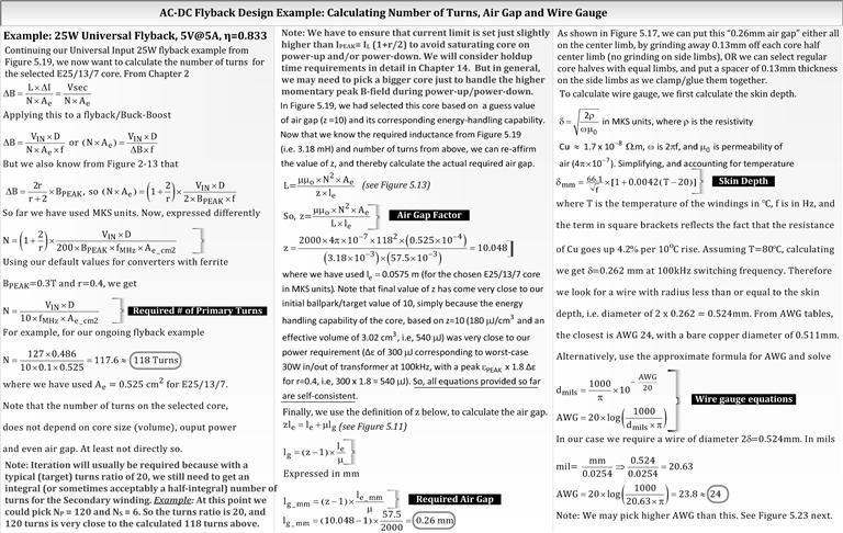
Figure 5.22: AC–DC flyback design example (part 2).
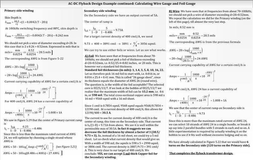
Figure 5.23: AC–DC flyback design example (part 3).
Part 5: More on AC–DC Forward Converter Transformer Design
In Chapter 3, we already have a detailed numerical example for Forward converter transformer design. The only thing missing there is now provided for the advanced reader: the derivations behind the design curves in Figures 3.10 and 3.11 (see Figures 5.24 and 5.25).

Figure 5.24: Dowell’s equations simplified and applied to switching power.
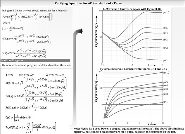
Figure 5.25: Dowell’s equations plotted out in a form useful for Forward converter design.