
Chapter 19
Solved Examples
This goes into several solved examples, culminating in a very detailed design of a Buck converter, including selection of components, estimation of losses and efficiency, thermal management, and feedback loop design.
Example 1
We have a non-synchronous Buck converter operating in continuous conduction mode (CCM). Its input is 12 V and output is 5 V. It uses a BJT switch with a forward drop VCE (sat)≡VSW=0.2 V. The catch diode is a Schottky device with forward drop VD=0.4 V. The load current is 1.5 A. What is the duty cycle? What is the dissipation in the BJT and in the diode? What is the estimated efficiency?
We set: VO=5 V, VIN=12 V, VD=0.4 V, VSW=0.2 V, IO=1.5 A.
![]()
Dissipation in the BJT and diode, and the total losses are
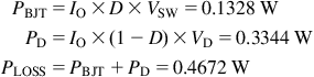
Note that we averaged the switch dissipation over a complete cycle by multiplying it by D, and similarly, averaged the diode dissipation by multiplying it by 1−D.
The output power, input power and efficiency are
![]()
![]()
Example 2
We have a non-synchronous Buck converter operating in continuous conduction mode (CCM). Its input is 12 V and its output is 5 V. It uses a FET switch with RDS=0.1 Ω. The catch diode is a Schottky device with forward drop VD=0.4 V. The load current is 1.5 A. What is the duty cycle?
We set: VO=5 V, VIN=12 V, VD=0.4 V, IO=1.5 A, RDS=0.1 Ω.
For a BJT, to a first approximation, we usually assume that its forward voltage drop is almost constant with respect to the current through it, which is the main reason why the BJT (along with its FET-driven cousin, the IGBT) is still often used in high-power applications. For a FET, the forward drop varies significantly, being considered virtually proportional to the current through it. In the simple duty cycle equation however, we need to plug in a certain fixed number “VSW.” So for a FET, we need to average the forward switch drop over the ON-time (note: here we do not average over the entire switching cycle). This is equivalent to taking the voltage drop corresponding to the average current through the switch during the on-time, which is simply the center-of-ramp (of the inductor current). Further, in a Buck topology, the center-of-ramp is equal to the load current IO. Hence, denoting ISW as the average current in the switch during the on-time (corresponding to the average drop VSW), we get
![]()
Example 3
What is the efficiency of the Buck converter in Example 2, if we disregard both the switch and diode drops?
Now we set: VO=5 V, VIN=12 V, VD=0 V, VSW=0 V, IO=1.5 A.
This leads to the “ideal” duty cycle equation for a Buck. We will also confirm that, in effect, it assumes 100% efficiency.
![]()
The input current of a Buck is the switch current averaged over the entire on-time. So, the input current corresponding to this duty cycle is
![]()
The corresponding input power is thus
![]()
The output power is
![]()
Therefore, the efficiency is 7.5 W/7.5 W=1 (i.e., 100%) as expected, validating our statement that if the switch and diode drops are set to zero, we get an “ideal” situation, with no losses.
Note: Of course, the only losses that were allowed in the first place, by the duty cycle equation currently in use in previous examples, are the losses related to the forward drops in the switch and diode, that is, the conduction losses in the semiconductors, no more. This indicates that since, quite obviously, not all switcher losses have been accounted for, the duty cycle equation in use so far is itself limited, and clearly just an approximation.
Example 4
What is the efficiency of the Buck converter in Example 2, if we disregard (only) the switch drop that is, we assume only a diode drop is present. Also, what is the loss in this diode?
We set: VO=5 V, VIN=12 V, VD=0.4 V, VSW=0 V, IO=1.5 A.
![]()
The input current of a Buck is the switch current averaged over the entire on-time. So, the input current corresponding to this duty cycle is
![]()
The corresponding input power is thus
![]()
The output power is clearly
![]()
Therefore, the efficiency is 7.5 W/7.8387 W=0.9568.
Now, the average diode current in a Buck is IO×(1−D). So, we get ID_AVG=1.5×(1−0.4355)=0.8468 A. The loss in the diode is therefore
![]()
We can see that this is exactly equal to the difference in input power and output power: PIN−PO=7.8387−7.5=0.3387 W, as expected. So, the balance sheet of losses is complete and accurate.
Example 5
In a Buck converter, we assume as above, that the switch is “ideal” (very low RDS), and the catch diode has a voltage drop of 0.4 V. If the efficiency of the converter is 95.679%, and the diode loss is 0.3387 W, what is the input power? What is the output power?
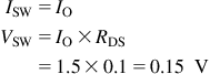
Here we are just working backwards. Further, we are not assuming any specific input and output voltages, or even a certain load current. We are just talking in terms of power. Looking at Figure 19.1, we see all the possible relationships between input and output power, versus loss and efficiency. Keep in mind these are valid equations for any power converter in general, not necessarily just switchers. We focus our attention on the lowermost diagram in the figure (under “In terms of loss”). To use the equations here, we need to know the loss, which in this example is the loss in the diode.
Figure 19.1: Power in, power out, power loss, and efficiency relations.
We set: PLOSS=0.3387 W, η=0.95679.
So,
![]()
![]()
This agrees with Example 4. We have thus validated the relevant equations in Figure 19.1 and also our previous calculations.
Example 6
In Example 4, correlate the diode dissipation to the additional energy drawn from the input and the increase in input current, as compared to the ideal case.
The diode loss was PD=0.3387 W. This must correspond to the additional energy per unit time drawn from the input. We recall from Example 3, that the ideal duty cycle was DIDEAL=0.4167. Now, with diode loss included, the duty cycle is D=0.4355. The general equation for the (average) input current of a Buck is IO×D. Note that in a Buck, the input current is the switch current averaged first over the on-time, that is, ISW≡IO, and then further averaged over the entire cycle (by multiplying it with D). So, for the ideal case, we get
![]()
However, for the non-ideal case (using the value of D calculated in Example 4)
![]()
The additional energy per unit time inputted when the duty cycle stretches out from its ideal value (in turn leading to the observed increase in input current) is
![]()
This is equal to the diode loss in Example 4. This thus validates the following general statement:
IIN_IDEAL is the baseline current level for a given PO and input/output, corresponding to all the incoming energy being fully converted into useful energy (i.e., no losses). As explained in Chapter 1 too, any increase above and beyond this baseline level, coincides exactly with the losses in the converter.
Example 7
Suppose we have a 12 to 5 V synchronous Buck, using a control FET with RDS of 1 Ω, and a synchronous FET with RDS of 0.8 Ω. The output current is 1.5 A. The inductor has a DC resistance (DCR) of 0.1 Ω. What is the duty cycle, the breakup of the losses, and the efficiency? Continue to ignore switching losses, as we have been doing so far.
We set: VO=5 V, VIN=12 V, RDS_1 =1 Ω, RDS_2=0.8 Ω, DCR=0.1 Ω.
Let us call the average current in the two FETs during the on-time (not averaged over the whole cycle) as “ISW_1” and “ISW_2”. So, since in a Buck, that is equal to the center-of-ramp IO, we get
![]()
The corresponding switch drops (i.e., their average values over the on-time) are
![]()
So, from the general duty cycle equation in Figure 19.2, with VD=VSW_2
![]()
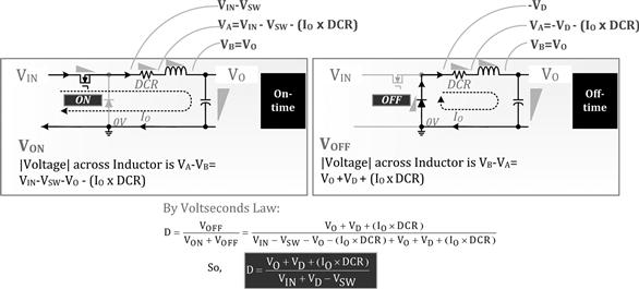
Figure 19.2: Buck duty cycle equations with DCR included.
The remaining calculations are
The computed efficiency is therefore η=PO/PIN=7.5/9.7692=0.7677 (i.e., 76.8%).
The losses are PIN−PO=2.2692 W. Let us confirm where this heat went.
We get the FET and inductor losses as
![]()
![]()
![]()
Summing up all loss terms:
![]()
This agrees with the difference in input and output power PIN−PO, thus validating our equations above.
Example 8
Design a wide-input 5 V output, at 5 A, DC–DC synchronous Buck with a switching frequency of 1 MHz. The target efficiency is greater than 80% at max load over the entire input voltage range of 9–57 V.
Having understood the underlying concepts in power conversion, we now do a complete top-down design of a typical wide-input Buck converter. After going through it, the average reader should also be able to complete a similar top-down design for the Boost and Buck-Boost topologies.
Start by assuming zero switch drops (ideal case). Call that duty cycle “DIDEAL.” The worst-case design point for a Buck inductor (max peak currents) is VINMAX (see Chapter 7). So, that is where we start our Buck design too.
![]()
As per the equations provided in the appendix
![]()
We have used the initial estimate for r at high line as rINITIAL_VINMAX=0.4. But now we need to pick a standard value of L and then recalculate the actual r at high line (and at low). Pick an inductor of standard value 2.2 μH. We thus get
![]()
Note that this is still an initial estimate, since it is based on the ideal duty cycle.
At minimum input voltage we have the following ideal duty cycle and corresponding r
![]()
![]()
Part 1: FET Selection
In the top (control) FET position, we prefer a P-channel FET so that we can avoid a bootstrap rail as discussed in Chapter 1. Of course, the controller IC selected must be commensurate with that desire.
The output power is 5 V×5 A=25 W. If we target an efficiency of over 80% over the entire operating input voltage range (not over the entire load range!), the input power is a max of 25/0.8=31.25 W. In other words, we are allowed a total loss of 6.25 W. To achieve a cost-effective design, we keep in mind that at low line, the top FET conducts for a longer time, whereas at high line, it is the bottom (synchronous) FET that conducts for a longer time. Since both FETs do not see a worst-case dissipation at the same input voltage extreme, we now set their individual dissipation targets to about 4 W (for their respective conduction loss components). The rest is for switching/crossover losses (in the top FET) and other miscellaneous losses like DCR-related losses, capacitor losses, and so on. Note that our FET selection here is based on efficiency targets, and is not directly based on current or temperature stresses. But those should be checked out too as discussed in Chapters 6 and 11. Note also that with this efficiency target, if the output voltage was not 5 V, but say, 1 V (as in many VRM applications nowadays), we would need to really choose FETs of much lower RDS. If the output voltage is low, for the same power, the currents are much higher. Further, since heating goes as I2R, to keep to within a certain power dissipation budget, the resistance “R” (RDS in our case) will need to be reduced significantly (~25 times in this example), and/or we will need to choose a much better package too, especially for the lower FET, since the thermal resistance of the currently selected one is rather high. Further, if we want to do 25 W with just 1 V output, that is at 25 A load current, we will actually need to use interleaved converters as discussed in Chapter 13.
For the current application, our first choices for FETs are:
(a) Top position, control FET, designated #1: P-channel FET, SUD08P06-155L from Vishay. This is rated 60 V and 6 A at 100°C case temperature; see also the discussion in Chapter 6 on FET current ratings. Its maximum (“hot”) RDS is 0.28 Ω.
(b) Bottom position, synchronous FET, designated #2: N-channel FET: IRFZ34S from Vishay or International Rectifier. This is rated 60 V and about 21 A at 100°C case temperature. Its max (room temperature) RDS is 50 mΩ, increasing by a factor×1.6 at high temperatures. So, we take its max (“hot”) RDS as 0.05×1.6=0.08 Ω.
We thus set RDS_1=0.28 Ω and RDS_2=0.08 Ω.
Note: We will see that the selected Drain-to-Source resistances of the two FETs are commensurate with the target dissipation. Observe that the load current is only 1.5 A, yet we have selected a 6 A FET for the top position, and a 21 A FET for the bottom position. However, the big increase in rating (i.e., lower RDS) of the bottom FET in particular is not only on account of the very low duty cycle at high line (its long conduction time) but also on the significantly worse thermal resistance characteristics it possesses as per its datasheet.
Note: It seems that the voltage stress factor is not sufficient since we are using a 60 V FET in a 57 V max application. However, keep in mind that both the selected FETs have guaranteed avalanche ratings, so they can absorb narrow spikes higher than 60 V. But the application must be evaluated thoroughly to ensure that this FET selection is acceptable.
Part 2: Conduction Losses in the FETs
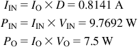
For the top FET, we expect the conduction loss to be worst at low line (because of the higher duty cycle). From Chapter 7 and the appendix, the switch RMS equation is
Its conduction loss at low line is therefore PCOND_1_VINMIN=3.73312×0.28=3.9021 W (using RDS_1=0.28 Ω).
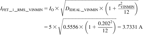
At high line, for the same FET, we get
Its conduction loss at high line is therefore PCOND_1_VINMAX=1.49142×0.28=0.6228 W (using RDS_1=0.28 Ω).
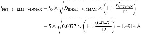
We now calculate the dissipation in the bottom FET, over both line extremes. We proceed as above, but with the appropriate RDS and with 1−D instead of D. For this FET we expect worst-case dissipation at high line because of the smaller converter duty cycle that translates into a larger on-time for this FET. At low line, the switch RMS current is
Its conduction loss is therefore PCOND_2_VINMIN=3.3392×0.08=0.8919 W (using RDS_2=0.08 Ω). At high line, its RMS current is
Its conduction loss is therefore PCOND_2_VINMAX=4.80982×0.08=1.8507 W (using RDS_2=0.08 Ω).
Finally, we get the total FET dissipation due to conduction losses only, at low and high line as (using the numbers highlighted below)
![]()
![]()
Note that even at low line, the RMS current in the bottom FET is comparable to that of the top FET, but because we have picked such a low RDS for the bottom FET, its dissipation is relatively lower at both line extremes. Remember that especially at high line, we still need to account for crossover losses in the top FET, as calculated further below.
Part 3: FET Switching Losses
We are following the steps in Chapter 8 (Figure 8.16 in particular). We are also trying to maintain most of that chapter’s terminology here.
We are assuming that crossover losses occur in the top FET only, as explained in Chapter 8.
As per datasheet of the top FET, we set Qgs=2.3 nC, Vt=2 V, g=8 S (Siemens, i.e., mhos).
![]()
Reading from the curves provided in the FET datasheet, we get a much lower value of Ciss=0.45 nF. Therefore, as explained in Chapter 8, we need to apply the following scaling (correction) factor (to account for the voltage coefficient of capacitance)
![]()
From the datasheet curves, we get Coss=0.06 nF and Crss=0.04 nF. We need to apply the same scaling factor to these numbers too. We have also expressed all these capacitances in pF rather than nF for the equations further below. So the final values used are
![]()
![]()
![]()
Finally, the capacitances we need, to calculate the intervals are

We also set a Gate drive voltage of 9 V. Assume this is very close to the minimum of the input voltage range. Keep in mind that, typically, we need a Gate drive voltage of about 10 V to drive the selected FETs properly (turn them ON fully), but 9 V will also suffice. We also assume the pull-up drive resistor is 2 Ω.
We set: Vdrive=9 V, Rdrive=2 Ω.
From Figures 8.7 to 8.10, we get the required durations/time constant as
![]()
![]()
![]()
![]()
Therefore, the crossover time during turn-on is (at either voltage extreme):
![]()
![]()
So, the crossover losses associated with turn-on, at both input extremes are
![]()
![]()
As expected, the crossover losses are higher at high line because of the higher voltage during crossover (combined with the fact that since this is a Buck, the center-of-ramp is fixed, irrespective of input voltage).
Next we calculate the losses associated with turn-off. We set the pull-down as Rdrive=1 Ω.
From Figures 8.11 to 8.14, we get the required time constant and durations as
![]()
![]()
![]()
![]()
Therefore, the crossover time during turn-off (at either voltage extreme) is
![]()
![]()
So, the crossover losses associated with turn-off are
![]()
![]()
The total crossover loss, therefore, is
![]()
![]()
However, to complete the switching loss term, we also have to add one more term to the crossover loss above. This is related to the regular dumping of the energy of Cds into the FET at every turn-on. We get, using Cds=38.94 pF (as calculated earlier)
![]()
![]()
So finally, the total switching loss terms at either input voltage extreme (occurring only in the top FET) are
![]()
![]()
Note that we have neglected the Gate driver losses calculated in Chapter 8, since they are relatively small, especially when doing dissipation calculations at max load. Driver losses do become significant at light loads, but we have not concerned ourselves with light-load efficiency in this example.
Adding the switching loss to the conduction loss of the top FET, we get the total loss in the top FET
![]()
![]()
The typical assumption is that the bottom FET has negligible switching losses. So,
![]()
![]()
Therefore, we get the combined dissipation in both FETs at both input extremes
![]()
![]()
Both these are well within the 6.25 W planned budget. But we still need to calculate and add a few more, relatively minor, loss terms.
Part 4: Inductor Loss
Our choice of inductance was 2.2 μH. We also know that its rating must be greater than 5 A. A suitable off-the-shelf inductor is therefore the 2.2 μH inductor “UP2C-2R2-R” from Coiltronics, rated 7.5 A. Its DCR is 6.6 mΩ and its maximum volt μ seconds is 9.6 at 300 kHz, corresponding to core losses that are 10% of the total losses for a 40°C rise in temperature.
We need to understand that the inductor has a ISAT rating of 8.67 A (which is sufficient in our application), and that the stated 7.5 A rating corresponds to the amount of DC current (no ripple and therefore no core loss) that can be passed through the inductor such that it produces a temperature rise of 40°C. In Chapter 2, we discussed ways of validating an off-the-shelf inductor in a particular application, and also estimating its core loss term. This particular vendor, however, provides an easy look-up chart for the purpose, as presented in Figure 19.3. The procedure to use it will become clear soon.
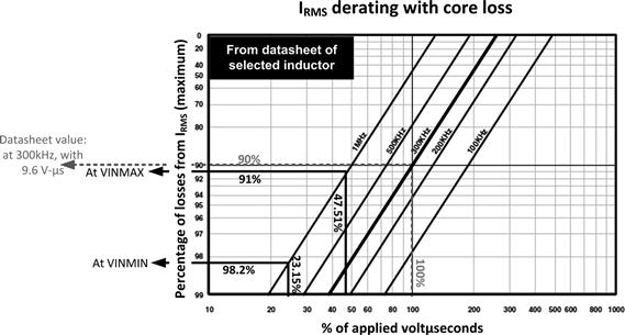
Figure 19.3: Estimating core losses in selected Coiltronics inductor.
First quantify the total permissible dissipation in the inductor. That is
![]()
To evaluate the core loss and IRMS derating in our application, we need to find out the applied voltμseconds (which we are hereby calling “Et” as we did in Chapter 2).
![]()
![]()
From the datasheet of the inductor, the rated voltμseconds is given by
![]()
So, the ratio of the applied voltμseconds to the rated value (at both lines extremes) is
![]()
![]()
Now looking at Figure 19.3, we see that with 47.15% of the rated voltμseconds and at 1 MHz switching frequency, the percentage of loss from the RMS heating is to be kept to about 91% of the total loss when both are combined to produce a 40°C rise. So basically, this means the total maximum (allowed) copper loss is now only 0.91×0.371 W=0.338 W. This corresponds to a certain reduction in the rated RMS to a value below 7.5 A, one that we can work out easily as presented further below. But right here, we don’t need that value. Because with the given information we can find out the core loss in our application. The logic is as follows: the reason for the required RMS derating is that the core loss makes up for the difference. So, it is easy to realize that the estimated core loss in our application (at high line) is 0.371 W−0.338 W=0.033 W. That makes it 9% of the total rated allowed dissipation (0.371 W) as expected. Similarly, at VINMIN, the applied voltμseconds is 23.15% of the rated voltμseconds. From Figure 19.3, we see that it intersects the y-axis at 98.2%. So, with the same logic, the core loss at low input voltage is 1.8% the total rated wattage, that is, 0.018×0.371=0.00668 W. We consolidate the results on core loss at both line extremes
![]()
Next, we calculate the actual copper loss in our application. But before we do that we should confirm that we are operating within the derated RMS rating of the inductor (with the above-mentioned core losses). If it turns out that the continuous max inductor current in our application is less than the derated rating, we can logically conclude that the inductor’s temperature rise will be less than 40°C; otherwise, it will be greater than 40°C (but that may also be acceptable depending on our worst-case ambient temperature). The derated RMS ratings at both line extremes (in our application) are obtained by the following steps.
(a) At VINMAX, the maximum allowed copper loss is 91% of the total allowed loss (0.371 W). Now, since the DCR is 6.6 mΩ, we get the budgeted copper loss as
![]()
Solving we get the maximum RMS rating
![]()
Since the applied RMS in our application is around 5 A (see below), it is well within the max derated rating and the temperature rise will therefore be less than 40°C.
![]()
The applied RMS is around 5 A as we see below, so it is well within the max derated rating.
The amount of RMS current in the inductor, as per the equations in Chapter 7 and the Appendix is

Note that as expected in a typical CCM inductor design, the RMS current is very close to the DC value (center-of-ramp), so it is not really necessary to use the RMS equation above. We could just use the DC value. The copper loss is
![]()
![]()
The total inductor loss is finally
![]()
![]()
Part 5: Input Capacitor Selection and Loss
We start by selecting the capacitor based on a target input voltage ripple of ±0.5% (typical of DC–DC integrated switchers and controller ICs). So, at an input of 57 V, that allows for a peak-to-peak input ripple of 1%×57=0.57 V. We are assuming that the maximum input ripple occurs at maximum input voltage (that statement is true for all topologies). From Chapter 13 we have seen that the actual ripple is a mixture of an ESR-based ripple component (ignoring ESL here) and a capacitance-based ripple component. Let us assume we want to pick a ceramic input capacitor with a typical (low) ESR of 50 mΩ (including lead and trace resistances). From Figure 13.4, we can solve for CIN:
We pick a standard cap of value of 2.2 μF, rated 63 V or higher. The RMS current in the input cap is (see Chapter 7 and Appendix)


Observe that this is consistent with Curve #4 in Figure 7.7, since the duty cycle closest to D=0.5 is at VINMIN in our application. The dissipation, therefore, is
![]()
![]()
Part 6: Output Capacitor Selection and Loss
We set ourselves the task of satisfying three constraints simultaneously, as shown below. The corresponding rationale and design equations are provided in Figure 19.4.
(1) Maximum peak-to-peak output ripple to be within 1% (i.e., ±0.5%) of output rail, that is, VO_RIPPLE_MAX=0.05 V.
(2) Maximum acceptable droop during a sudden increase in load: ΔVDROOP=0.25 V.
(3) Maximum acceptable overshoot during a sudden decrease in load: ΔVOVERSHOOT=0.25 V.
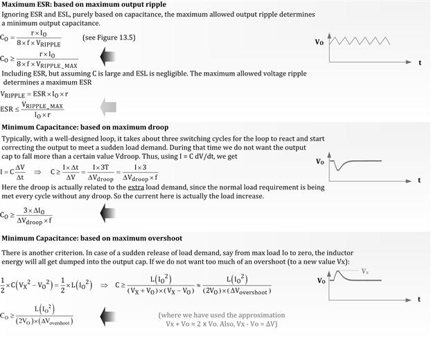
Figure 19.4: Criteria for output capacitor of a Buck converter.
We have minimum output capacitances based on (1), (2), and (3) above, as follows:
![]()
![]()
![]()
Let us therefore pick a standard output capacitance of 33 μF (rated 6.3 V or higher).
![]()
We should also double check that the ESR of the selected cap is small enough. As per Figure 7.7, we check the ESR-based portion of the ripple at high line. Refer to Figure 13.5 for the output ripple equations. The ESR should be less than
![]()
Most ceramic capacitors will have no trouble complying with this. Suppose we pick a capacitor with ESR=20 mΩ. To calculate dissipation, we need to find out the RMS current in the output cap.
![]()
![]()
![]()
![]()
Part 7: Total Losses and Efficiency Estimate
We can now sum over the losses in the FETs, inductor, and input/output capacitors.
![]()
![]()
Estimated efficiency is
![]()
![]()
We see that we have achieved our target of greater than 80% efficiency over the entire input range.
Note that so far we have done the calculations based on the ideal duty cycle equation. Actually, we are now in a position to calculate duty cycle more accurately — based on efficiency as explained in Chapter 5. We can then use the new values of duty cycle to run through the above equations once again if we want. Repeated iterations will yield progressively more accurate predictions of efficiency. The improved equations for duty cycle are
![]()
![]()
Compare the values so obtained to the ideal values of 0.088 and 0.556, respectively. We realize based on the preceding examples, that this increase in duty cycle corresponds with the total loss occurring in the converter.
Part 8: Junction Temperature Estimates
Let us assume that the FETs are mounted reasonably far away from each other, so there are no hot-spots (thermal constriction effects). We also assume that the copper area is large enough (say, a two-sided board, with thermal vias passing through to the copper side below the FETs, and so on).
As per the datasheet of the top FET, we can assume a typical junction to ambient thermal resistance of 25°C/W, and for the bottom FET we assume 40°C/W. We also assume that the local ambient (in the vicinity of the FETs) is 15°C higher than the max room ambient of 40°C. So for the FETs, the effective max ambient is 55°C. We also know that the worst-case for the top FET is at low line, and for the bottom FET at high line. We thus estimate the following worst-case junction temperatures for the top and bottom FETs, respectively.
![]()
![]()
Both the FETs are rated for a max junction temperature of 175°C, so the above temperatures are considered quite acceptable, though the top FET is running a little too hot (80% temperature derating is a max junction temperature of 0.8×175=140°C).
Part 9: Control Loop Design
We need to refer to Chapter 12 here, in particular Figures 12.25 and 12.26. We assume that the controller is a current mode IC and that it uses a “gm” error amplifier (OTA). Since the switching frequency is 1 MHz, we target a crossover frequency of fsw/3=333 kHz in keeping with the generic guidelines of current mode control. The max current is 5 A and the time period (of switching) is 1 μs.
(1) Slope Compensation
Let us assume the IC has a slope compensation of 1.5 A/μs. We want to first rule out subharmonic instability at maximum D and also at D=50% (because, remember that three conditions are required for enabling subharmonic instability: current mode control, CCM, and duty cycle exceeding 50%). As per Figure 12.24, the minimum inductances required to avoid this instability at max D and D=50%, respectively, are
![]()
![]()
In the latter equation we have used the fact that at D=50%, the input equals twice the output. Note also that we have used the freshly computed value of max duty cycle above, based on the preceding power and efficiency estimates.
Our selected inductance is 2.2 μH, so we will not suffer from subharmonic instability with the amount of slope compensation provided. But if that were not true, we would have needed to increase the inductance and/or the slope compensation.
(2) Load Pole and Plant Transfer Function
We are looking at Figure 12.25 here. The load pole “fp” is approximately 1/(2πRCO), but we are going to do a more exact calculation based on 1/(2πACO). “A” involves either the up-slope or the down-slope of the inductor current (expressed in Amps/μs). We work it all out here.
The down-slope is
![]()
Let us find “m” as defined in Figure 12.25, at both voltage extremes.
![]()
![]()
So “A” as defined in Figure 12.25 is (at both voltage extremes)
where we have used the following value for the load resistor R=VO/IO=5/5=1 Ω. Note that the use of “A” instead of R for finding fp, leads to a more accurate estimate of the location of the load pole. In our application, we see that “A” has a value between 0.8 and 0.9 Ω, that is, slightly less than R=1 Ω. So, in effect, it pushes out the load pole to a frequency slightly higher than that expected on the basis of the simplified (and more commonly used) value of fp≈1/(2πRCO). We thus get
![]()
![]()
Even though the load pole varies somewhat due to line voltage (because “A” varies too), the line rejection is still very good, and that is a key property of current mode control. With voltage mode control we would need to validate the control loop design at both the worst-case input extremes, even though the selection of components would obviously have to be based on one input voltage.
In Figure 12.23, we have defined the mapping resistor “Rmap.” This is the characteristic resistor of current mode control, relating the sensed current to the corresponding sensed voltage. Let us assume the total control voltage range (swing) is 1 V, and that it occurs in response to a change in sensed FET current ranging from 0 A to 5 A (no load to full load). In effect, Rmap is therefore 1 V/5 A=0.2 Ω. Now, we will use this information to calculate “B” in Figure 12.25. For a Buck, “B” equals Rmap. So we write
![]()
We can then calculate GO, the DC gain of the plant at both line extremes
![]()
![]()
In terms of decibels, using 20×log (GO), we get 12.31 dB and 12.97 dB, respectively.
We have all the information to plot the plant transfer function if required.
(3) Compensation Using an OTA
Now we will complete the feedback section, using a gm-amp. First, we find the attenuation ratio “y” in Figure 12.26. This is the step-down ratio provided by the gm-amp. Note that this step is different from a standard error amplifier as explained in Figure 12.12.
![]()
We have assumed the reference voltage is 1 V. So, for example, in the voltage divider we could be using 4k as the upper resistor and 1k as the lower one (or 10k and 2.5k, and so on).
We also have an important math relationship in Figure 19.5. Using that, at both voltage extremes, we get
![]()
![]()
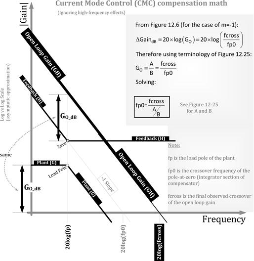
Figure 19.5: A math relationship for current mode control compensation.
Using the relationships in Figure 12.26 we get two recommendations for each voltage extreme, based on a selected gm=0.2 (but note that typically, OTAs have much smaller gm values!)
![]()
![]()
We see good line rejection at wok as expected. We just pick a close standard value to both.
In Figure 12.26, we see than the location of the zero “fz1” is 1/(2πR1C1). As per Figure 19.5, we set it at the location of the load pole. So we are setting fp=1/(2πR1C1). Since we know C1 from above, we can solve for R1 as follows
![]()
![]()
Once again, we just pick a close standard value.
Set R1=333Ω.
The pole fp1 in Figure 12.26 is set to cancel the ESR zero of the output cap (ESR=20 mΩ).
The ESR zero frequency is fESR=1/(2π×ESR×CO)=241.14 kHz. We thus get
![]()
We pick a standard value.
Set C2=2 nF.
We can plot the final results out, based on Figure 12.22 and the selected compensation components. We thus arrive at Figure 12.6, validating our selection and procedure (Figure 19.6).
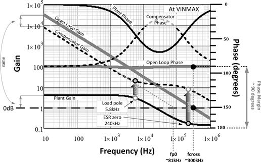
Figure 19.6: Plotting out the final results of the loop compensation.