
Chapter 4
The Topology FAQ
This chapter presents quick FAQs (frequently asked questions) to clarify and solidify all the concepts presented so far. It not only covers the key topologies but also includes new topics like low-side current sensing and maximum duty cycle considerations. It also provides quick lookup tables for calculating the average current flowing at different points in the three basic topologies. It is recommended to read this chapter before moving on to the more advanced chapters that follow.
This section serves to highlight and summarize the gamut of key topology-related design issues that should be kept in mind when actually designing converters (or when appearing for a job interview!).
Questions and Answers
Question 1: For a given input voltage, what output voltages can we get in principle, using only basic inductor-based topologies (Buck, Boost, and Buck-Boost)?
Answer: The Buck is a step-down topology (VO<VIN), the Boost only steps-up (VO>VIN), and the Buck-Boost can be used to either step-up or step-down (VO<VIN, VO>VIN). Note that here we are referring only to the magnitudes of the input and output voltages involved. So, we should keep in mind that the Buck-Boost inverts the polarity of the input voltage.
Question 2: What is the difference between a topology and a configuration?
Answer: We know that, for example, a “down-conversion” of 15 V input to a 5 V output is possible using a Buck topology. But what we are referring to here is actually a “positive-to-positive” Buck configuration, or simply, a “positive Buck.” If we want to convert –15 V to –5 V, we need a “negative-to-negative” Buck configuration, or simply, a “negative Buck.” We see that a topology is fundamental (e.g., the Buck) — but it can be implemented in more than one way, and these constitute its configurations.
Note that in the down-conversion of –15 V to –5 V, we use a Buck (step-down) topology, even though mathematically speaking, –5 V is actually a higher voltage than –15 V! Therefore, only magnitudes are taken into account in deciding what the nature of a power conversion topology is.
Similarly, a conversion of say 15 V to 30 V would require a “positive Boost,” whereas –15 V to –30 V would need a “negative Boost.” These are the two configurations of a Boost topology.
For a Buck-Boost, we need to always mentally keep track of the fact that it inverts the polarity (see next question).
Question 3: What is an “inverting” configuration?
Answer: The Buck-Boost is a little different. Although it has the great advantage of being able to up-convert or down-convert on demand, it also always ends up inverting the sign of the output with respect to the input. That is why it is often simply referred to as an “inverting topology.” So, for example, a “positive-to-negative” Buck-Boost would be required if we want to convert 15 V to −5 V or say to −30 V. Similarly, a “negative-to-positive” Buck-Boost would be able to handle −15 V to 5 V or to 30 V. Note that a Buck-Boost cannot do 15 V to 5 V for example, nor can it do −15 V to −5 V. The convenience of up- or down-conversion (on demand) is thus achieved only at the expense of a polarity inversion — the conventional (inductor-based) Buck-Boost topology is useful only if we either desire, or are willing to accept, this inversion.
Question 4: Why is it that only the Buck-Boost gives an inverted output? Or conversely, why can’t the Buck-Boost ever not invert?
Answer: In all topologies, there is a voltage reversal across the inductor when the switch turns OFF. So, the voltage at one end of the inductor “flips” with respect to its other end. Further, when the switch turns OFF, the voltage present at the swinging end of the inductor (i.e., the switching node) always gets “passed on” to the output, because the diode is then conducting. But in the case of the Buck-Boost, the “quiet end” of its inductor is connected to the ground reference (no other topology has this). Therefore, the voltage reversal that takes place at its other end (swinging end) is also a voltage reversal with respect to ground. And since this is the voltage that ultimately gets transmitted to the output (which is also referenced to ground), the reversal is virtually “seen” at the output. See Figure 1.15.
Of course the output rail continues to stay inverted even when the switch turns ON, because the diode then stops conducting, and there is an output capacitor present, that holds the output voltage steady at the level it acquired during the switch off-time.
Question 5: Why do we always get only up-conversion from a Boost converter?
Answer: Inductor voltage reversal during a switch transition occurs in all DC–DC switching topologies — it just does not necessarily lead to an output reversal. But in fact, inductor voltage reversal is responsible for the fact that in a Buck, the input voltage is always stepped-down, whereas in a Boost, it is stepped-up. It all depends on where the “quiet” end of the inductor connects to. In the Boost, the “quiet” end connects to the input rail (in the Buck, to the output rail). Therefore, since the swinging end of the Boost inductor is connected to ground during the switch on-time, it then flips with respect to the input rail during the switch off-time, gets connected to the output through the conducting diode, and thereby we get a boosted output voltage. See Figure 1.15.
Question 6: What is really “ground” for a DC–DC converter?
Answer: In a DC–DC converter there are two input rails and two output rails. But one of these rails is common to both the input and output. This rail is the (power) “ground.” The input and output voltages are measured with respect to this (reference) rail, and this gives them their respective magnitude and polarity. See Figures 1.12 and 1.14.
Question 7: What is “ground” for the control IC?
Answer: The reference rail, around which most of the internal circuitry of the IC is built, is its local (IC) ground. This rail comes out of the package as the ground pin(s) of the IC. Usually, this is connected on the PCB directly to the power ground (the common reference rail described above). However, there are exceptions, particularly when an IC meant primarily for a certain topology (or configuration) is rather unconventionally configured to behave as another topology altogether (or just a different configuration). Then the IC ground may in fact differ from the power ground. See Figure 9.17.
Question 8: What is “system” ground?
Answer: This is the reference rail for the entire system. So in fact, all on-board DC–DC converters present in the system usually need to have their respective (power) grounds tied firmly to this system ground. The system ground in turn usually connects to the metal enclosure, and from there on to the “earth (safety) ground” (i.e., into the mains wiring).
Question 9: Why are negative-to-negative DC–DC configurations rarely used?
Answer: The voltages applied to and/or received from on-board DC–DC converters are referenced by the rest of the system to the common shared system ground. By modern convention, all voltages are usually expected to be positive with respect to the system ground. Therefore, all on-board DC–DC converters also need to comply with the same convention. And that makes them necessarily positive-to-positive converters.
Question 10: Why are inverting DC–DC converters rarely used?
Answer: We usually cannot afford to let any given on-board converter attempt to “redefine” the ground in the middle of a system. However, inverting regulators can on occasion be used, especially if the converter happens to be a “front-end” converter. In this case, since the system effectively starts at the output terminals of this converter, we may be able to “define” the ground at this point. In that case, the relative polarity between the input and output of the converter may become a “don’t care” situation.
Question 11: Can a Buck regulator be used to convert a 15 V input to 14.5 V output?
Answer: Maybe, maybe not! Technically, this is a step-down conversion, since VO<VIN. Therefore, in principle, a Buck regulator should have worked. However, in practice there are some limitations regarding how close we can set the output of a converter in relation to the input.
Even if the switch of a Buck regulator is turned fully ON (say in an all-out effort to produce the required output), there will still be some remaining forward drop across the switch, VSW, and this would effectively subtract from the applied input VIN. Note that in this fully ON state, the switcher is basically functioning just like a “low dropout” regulator, or “LDO,” and so the concerns expressed in Chapter 1 regarding the minimum achievable headroom of an LDO apply to the switcher too in this state. As an example — if the switch drop VSW is 1 V then we certainly can’t get anything higher than 14 V output from an input of 15 V.
The second consideration is that even if, for simplicity, we assume zero forward voltage drops across both the switch and the diode, we still may not be able to deliver the required output voltage — because of maximum duty cycle limitations. So for example, in our case, what we need is a (theoretical) duty cycle of VO/VIN=14.5 V/15 V=0.97, that is, 97%. However, many Buck ICs in the market are not designed to guarantee such a high duty cycle. They usually come with an internally set maximum duty cycle limit (“DMAX”), typically around 90 to 95%. And if that is so, D=97% would be clearly out of their capability. Buck switchers with a P-channel MOSFET can usually do 100% duty cycle.
A good power supply designer also always pays heed to the tolerance or spread of the published characteristics of a device. This spread is usually expressed as a range with a specified “min” (minimum), a “max” (maximum), and a “typ” (typical, or nominal). For example, suppose a particular IC has a published maximum duty cycle range of 94–98%, we cannot guarantee that all production devices would be able to deliver a regulated 14.5 V — simply because not all of them are guaranteed to be able to provide a duty cycle of 97%. Some parts may manage 97%, but a few others won’t go much beyond a duty cycle maximum of 94%. So, what we need to do is to select an IC with the published “min” of its tolerance range greater than the desired duty cycle. For example, a Buck IC with a published DMAX range of 97.5–99% may work in our current application.
Why did we say “may” above? If we include the forward drops of the switch and diode in our calculation, we actually get a higher duty cycle than the 97% we got using the “ideal” equation D=VO/VIN. The latter equation implicitly assumes VSW=VD=0 (besides ignoring other key parasitics like the inductor’s DCR). So, the actual measured duty cycle in any application may well be a couple of percentage points higher than the ideal value.
In general, we should remember that whenever we get too close to the operating limits of a control IC, we can’t afford to ignore key parasitics. We must also account for temperature variations, because temperature may affect efficiency, and thereby the required duty cycle.
Question 12: What role does temperature play in determining the duty cycle?
Answer: As mentioned in Chapter 1, it is generally hard to predict the overall effect of temperature on a power-supply’s efficiency, and thereby on its duty cycle variation with respect to temperature. Some loss terms increase with temperature and some decrease. However, to be conservative, we should at a minimum account for the increase in the forward drop of the metal oxide semiconductor field effect transistor (MOSFET) switch. For low-voltage MOSFETs (rated ~30 V), the increase in RDS (on-resistance) in going from room temperature to “hot” is typically 30–50%. So, we typically multiply the published room temperature on-resistance by 1.4. For high-voltage MOSFETs, as used in off-line power supplies, the increase is about 80–100%. So, we typically multiply the room temperature on-resistance by 1.8.
Question 13: How can we convert an unregulated input of 15 V to a regulated output of 15 V?
Answer: The term “unregulated” implies that the stated value just happens to be the “typical” (usually center) of a certain range, which may or may not yet have been defined. So, an “unregulated input of 15 V” could well mean say 10–20 V, or 5–25 V, or 12–18 V, and so on. Anything that includes 15 V is possible.
Of course, ultimately, we do need to know what this input range really is. But it should already be apparent that for a “15 V to 15 V conversion”, if the input falls at the lower end of its range, we would need to up-convert, and if the input is at its upper end, we would need to down-convert. Therefore, we must choose a topology capable of performing both step-up and step-down conversions on demand.
How about the Buck-Boost? Unfortunately, the standard inductor-based Buck-Boost also gives us an inverted output, which we really don’t want here. What we need is a non-inverting step-up/step-down topology. Looking, a suitable candidate for this is the “SEPIC” (single-ended primary inductance converter) topology (see Figures 4.1, 9.14 and 9.15). It is best visualized as composite topology — a Boost stage followed by a Buck cell. Though this “Boost-Buck” combination needs only one switch, it requires an additional inductor, and also entails significantly more design complexity. We may therefore wish to consider a derivative (or variant) of the conventional Buck-Boost topology, but with the inductor replaced by a transformer. In effect, what we are doing is — we are first separating (isolating) the input from the output, and then reconnecting the windings of the transformer in an appropriate manner so as to correct for the inversion. Thus, we get a non-inverting or “non-isolated transformer-based Buck-Boost” — sometimes simply called a “flyback” topology.
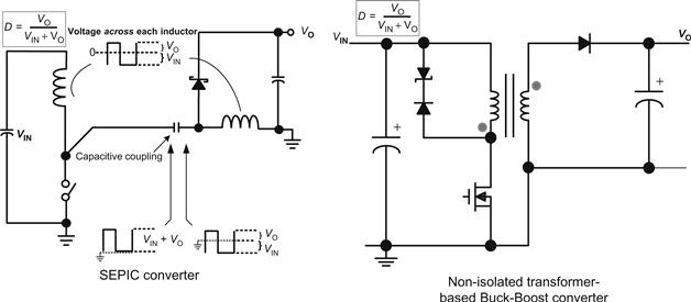
Figure 4.1: Positive-to-positive step-up/step-down converters.
Question 14: It is much easier to find “off-the-shelf” inductors. So why is a transformer-based Buck-Boost even worth considering?
Answer: It is true that most designers prefer the convenience of off-the-shelf components, rather than custom-designed components (like transformers). However, high-power off-the-shelf inductors often come with two identical windings wound in parallel (on the same core), (though that may not be immediately apparent just by looking at the datasheet). Further, the ends of these two windings are sometimes completely separated from each other (no galvanic connection between the windings). The reason for this may be that from a production standpoint, it doesn’t make sense to try to solder too many copper strands on to a single pin/termination. So, the intention here is that the two windings will be eventually connected to each other on the PCB itself. But sometimes, the intention of leaving separate windings on an inductor is to allow flexibility for the two windings to be connected to each other either in series, or in parallel, as desired. So for example, if we place the windings in series, that would reduce the current rating of the inductor (originally, each winding was expected to carry only half the rated current), but we would get a much higher inductance. If in parallel, the inductance would come down, but the current rating would increase. However, in low-voltage applications, where safety isolation is not a concern, we can also exploit this inductor structure and use it as a 1:1 transformer for correcting the polarity inversion of the Buck-Boost.
Question 15: In an inductor with split windings (1:1), how exactly does its current rating and its inductance change as we go from a parallel configuration to a series configuration?
Answer: Suppose each winding has 10 turns and a DC resistance (DCR) of 1 Ω. Now, if it is used in parallel configuration, we still have 10 turns, but the effective DCR is 1 Ω in parallel with 1 Ω, i.e., 0.5 Ω. When a series configuration is used, we get 2 Ω and 20 turns. We also know that inductance depends on the square of the number of turns. So, that goes up four times.
What about the current rating? This is largely determined by the amount of heat dissipation the inductor can tolerate. But its thermal resistance (in °C/W) is not determined by the winding configuration, rather by the exposed area of the inductor, and other physical characteristics. Therefore, whether in series or in parallel configuration, we have to maintain the same total I2R loss. For example, suppose we call the current rating in parallel as “IP”, and in series “IS,” then as per the DCR in our above numerical example, we get
![]()
So,
![]()
Therefore, in going from a parallel to a series configuration, the inductance will quadruple and the current rating will halve.
What happens to the B-field? Don’t we have to consider the possibility of saturation here? Well, B is proportional to LI/N (see Figure 2.13). So, if inductance quadruples, I halves, and N doubles, the B-field is unchanged!
Question 16: Is there any difference between the terms “Buck-Boost” and “flyback”?
Answer: The answer to that may well depend on whom you ask! These terms are often used interchangeably in the industry. However, generally, most people prefer to call the conventional inductor-based version a (true) “Buck-Boost,” whereas its transformer-based version, isolated or non-isolated, is called a “flyback.”
Question 17: When and why do we need isolation? And how do we go about achieving it?
Answer: We must recognize that a (transformer-based) flyback topology may or may not provide us with isolation. Isolation is certainly a natural advantage accruing from the use of a transformer. But to preserve isolation, we must ensure that all the circuitry connected to the switch side of the transformer (“Primary side”) is kept completely independent from all the circuitry sitting on the output side (“Secondary side”) (see Figure 1.1 in Chapter 1).
So for example, if in our attempt to correct the polarity inversion of a Buck-Boost we make a connection between the Primary and Secondary windings of the transformer, we lose isolation. But if our intention is to reset polarity, that would be acceptable.
To maintain isolation, besides making no galvanic connection between the power stages on either side of the transformer, we must not make any signal-level inter-connections either. However, we must carry the feedback signal (or any fault information) from the output side to the IC, via one or more “optocouplers.” The optocoupler manages to preserve Primary-to-Secondary voltage isolation, but allows signal-level information to pass through. It works by first converting the Secondary-side signal into radiation (light) by means of an “LED” (light-emitting diode), beaming it over to the Primary side onto a photo-transistor, and thereby converting the signal back into electrical impulses (all this happening within the package of the device itself).
In high-voltage applications (anything over 60 V DC, e.g., off-line power supplies), it is in fact required by law, to provide electrical isolation between a hazardous input voltage level and any user-accessible (“safe”) metal surfaces (e.g., output terminals of the power supply). Therefore, there is a “Primary ground” at the input side of the transformer, and a separate “Secondary ground” on the output side. The latter is tied to the ground of the system, and usually also to the earthed metal enclosure.
Question 18: In an off-line power supply, are the Primary and Secondary sides really completely isolated?
Answer: It is interesting to note that safety regulations specify a certain physical spacing that must be maintained between the Primary and Secondary sides — in terms of the RMS of the voltage differential that can be safely applied between them. The question arises — how do we define a voltage difference between the two sides of a transformer that are supposedly separate anyway? What is the reference level to compare their respective voltages? After all, voltage is essentially a relative term.
In fact the two sides do share a connection! As mentioned, the Secondary-side ground is usually the system ground, and it connects to the metal enclosure and/or to the ground wire of the mains supply (“earth” or “safety ground”). But further down the AC mains distribution network, the safety ground wire is connected somewhere to the “neutral” wire of the AC supply. And we know that this neutral wire comes back into the Primary side. So in effect, we have established a connection between the Primary and Secondary sides. It does not cause the user any problem, because he or she is also connected to earth. In effect, the earth potential forms the reference level to establish the voltage difference across the safety transformer, and to thereby fix the Primary-to-Secondary spacing, and also the breakdown rating of any Primary-to-Secondary insulation.
Note that in some portable equipment, only a two-wire AC cord is used to connect it to the mains supply. But the spacing requirement is still virtually unchanged, since a user can touch accessible parts on the Secondary side and complete the connection through the earth ground.
Question 19: From the standpoint of an actual power supply design procedure, what is the most fundamental difference between the three topologies that must be kept in mind?
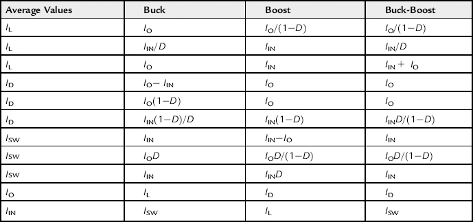
Answer: In a Buck, the average inductor current (“IL”) is equal to the load current (“IO”), that is, IL=IO. But in a Boost and a Buck-Boost, this average current is equal to IO/(l–D). Therefore, in the latter two topologies, the inductor current is a function of D (duty cycle) — and therefore indirectly a function of the input voltage too (for a given output).
Question 20: In the three basic topologies, how does the duty cycle change with respect to input voltage?
Answer: For all topologies, a high D corresponds to a low-input voltage, and a low D to a high input.
Question 21: What do we mean by the “peak current” of a DC–DC converter?
Answer: In any DC–DC converter, the terms “peak inductor current,” “peak switch current,” and “peak diode current” are all the same — referred to simply as the peak current “IPK” (of the converter). The switch, diode and inductor have the same peak current value.
Question 22: What are the key parameters of an off-the-shelf inductor that we need to consider?
Answer: The inductance of an inductor (along with the switching frequency and duty cycle) determines the peak current, whereas the average inductor current is determined by the topology itself (and the specific application conditions — the duty cycle and load current). For a given application, if we decrease the inductance, the inductor current waveform becomes more “peaky,” increasing the peak currents in the switch and diode too (also in the capacitors). Therefore, a typical converter design should start by first estimating the optimum inductance so as to avoid saturating the inductor. That is the most basic concern in designing/picking an inductor.
However, inductance by itself doesn’t fully describe an inductor. In theory, by choosing a very thin wire gauge, for example, we may be able to achieve almost any inductance on a given core, just by winding the appropriate number of turns. But the current that the inductor will be able to handle without saturating is still in question, because it is not just the current, but the product of the current and the number of turns (“Ampere-turns”) that determine the magnetic field present in the inductor core — which in turn determines whether the inductor is saturating or not. Therefore, we need to look out for an inductor with the right inductance and also the required energy handling capability, usually expressed in μJ (microJoules). This must be greater than or equal to the energy it needs to store in the application, ![]() . Note that the “L” carries with it information about the number of turns too, since L∝N2, where N is the number of turns. See Chapter 5.
. Note that the “L” carries with it information about the number of turns too, since L∝N2, where N is the number of turns. See Chapter 5.
Question 23: What really determines the current rating of an inductor?
Answer: There are two limiting factors here. One is the heat developed (I2R losses), which we should ensure is not excessive (typically causing a temperature rise of 50°C or less). The second is the magnetic field it can withstand without saturating. So, most ferrites allow a maximum B-field of about 3,000 G before saturation starts.
Question 24: Does the maximum allowable B-field depend on the air gap used?
Answer: When designing (gapped) transformers, we need to remember that first, the B-field present within the core material (e.g., ferrite) is the same as the B-field in the air gap. It does not change. Second, though by changing the air gap we may end up decreasing the existing B-field, the maximum allowable B-field depends only on the core material used — it remains fixed, for example, at about 3,000 G for ferrites. Note that the H-field is defined as H=Β/μ, where μ is the permeability of the material. Now, since the permeability of ferrite is much higher than that of air, and the B-field is the same in both, therefore the H-field is much lower in the ferrite than in the air gap.
Question 25: Why is it commonly stated that in a flyback transformer, the “air gap carries most of the stored magnetic energy”?
Answer: We can intuitively accept the fact that the energy stored is proportional to the volume of the magnetic material. And because of that, we also tend to think the ferrite must be carrying most of the energy, since it occupies the maximum volume — the amount of air enclosed between the ends of the ferrite being very small. However, the stored energy is also proportional to B×H, and since the H-field in the gap is so much larger, it ends up storing typically two-thirds of the total energy, despite its much smaller volume.
Question 26: If air carries most of the stored energy, why do we even need the ferrite?
Answer: An air-cored coil would seem perfect as an inductor, especially since it would never saturate. However, the number of turns required to produce a given inductance would be impractically large, and so we would get unacceptable copper losses. Further, since there is nothing to “channel” (constrain) the flux lines, the air-cored inductor would spew electromagnetic interference (EMI) everywhere.
The ferrite is useful, because it is the very means by which we can create such high magnetic fields in the first place — without an excessive number of turns. It also provides us the “channel” for flux lines that we had been looking for. In effect, it “enables” the air gap.
Question 27: What is the basic design rule for calculating inductance for all the topologies?
Answer: To reduce stresses at various points inside a power supply, and also to generally reduce the overall size of its components, a “current ripple ratio” (“r”) of about 0.4 is considered to be a good compromise for any topology, at any switching frequency.
“r” is the ratio ΔI/IL, where ΔI is the swing in the current, and IL is the average inductor current (center of the swing ΔI). An r of 0.4 is the same as r=40%, or r=±20%. This means that the peak inductor current is 20% above its average value (its trough being 20% below).
To determine the corresponding inductance we use the definition r=ΔI/IL, along with the inductor equation, to get
![]()
solving
![]()
This gives us the inductance in Henrys, when f is in Hz. Note that VON is the voltage across the inductor when the switch is ON. It is therefore equal to VIN–VO for a Buck, and VIN for a Boost and a Buck-Boost. Also, IL is the average inductor current, equal to IO for a Buck, and IO/(1–D) for a Boost and a Buck-Boost.
Question 28: What is a “Forward converter”?
Answer: Just as the isolated flyback is a derivative of the Buck-Boost topology, the Forward converter is the isolated version (or derivative) of the Buck topology. It too uses a transformer (and optocoupler) for providing the required isolation in high-voltage applications. Whereas the flyback is typically suited for output powers of about 75 W or less, the Forward converter can go much higher.
The simplest version of the Forward converter uses only one transistor (switch), and is thus often called “single-ended.” But there are variants of the single-ended Forward converter with either two or four switches. So, although the simple Forward converter is suited only up to about 300 W of power, we can use the “double-switch Forward converter” to get up to about 500 W. Thereafter, the half-bridge, push–pull, and full-bridge topologies can be exploited for even higher powers (see Figure 4.2 and Table 7.1). But note that all of the above topologies are essentially “Buck-derived” topologies.
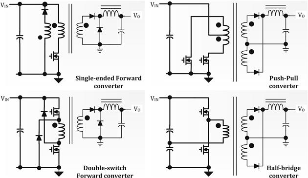
Figure 4.2: Various Buck-derived topologies.
Question 29: How can we tell whether a given topology is “Buck-derived” or not?
Answer: The simplest way to do that is to remember that only the Buck has a true LC filter at its output. There is nothing separating the inductor and the output capacitor.
Question 30: Which end of a given input voltage range VINMIN to VINMAX should we pick for starting a design of a Buck, a Boost, or a Buck-Boost converter?
Answer: Since the average inductor current for both the Boost and Buck-Boost increases as D increases (IL=IO/(1–D)) — the design of Boost and Buck-Boost inductors must be validated at the lower end of the given input range, that is, at VINMIN — since that is where we get the highest (average and peak) inductor current. We always need to ensure that any inductor can handle the maximum peak current of the application without saturating. For a Buck, the average inductor current is independent of the input or output voltage. However, observing that its peak current increases at higher input voltages, it is preferable to design a Buck inductor at VINMAX.
Question 31: Why are the equations for the average inductor current of a Boost and a Buck-Boost exactly the same, and why is that equation so different from that of a Buck?
Answer: In a Buck, energy continues to flow into the load (via the inductor) during the entire switching cycle (during the switch on-time and off-time). Therefore, the average inductor current must be equal to the load current, that is, IL=IO.
Note that capacitors contribute nothing to average current flow, because, in steady state, just as the voltseconds across an inductor averages out to zero at the end of each cycle, the charge in a capacitor does likewise (charge is the integral of current over time, and has the units Amperes-seconds). If that did not happen, the capacitor would keep charging up (or discharging) on an average, until it reaches a steady state.
However, in a Boost or Buck-Boost, energy flows into the output only during the off-time. And it comes via the diode. So, the average diode current must be equal to the load current. By simple arithmetic, since the average diode current calculated over the full cycle is equal to IL×(1–D), equating this to the load current IO gives us IL=IO/(1–D) for both the Boost and the Buck-Boost.
Question 32: What is the average output current (i.e., the load current) equal to for the three topologies?
Answer: This is simply the converse of the previous question. For the Buck, the average output current equals the average inductor current. For the Boost and Buck-Boost, it is equal to the average diode current.
Question 33: What is the average input current equal to for the three topologies?
Answer: In a Buck, the input current flows only through the switch. It stops when the switch turns OFF. Therefore, the average input current must be equal to the average switch current. To calculate the average of the switch current, we know it is ON for a fraction D (duty cycle) of the switching cycle, during which time it has an average value (center of ramp) equal to the average inductor current, which in turn is equal to the load current for a Buck. Therefore, the average of the switch current must be D×IO, and this must be equal to the input current IIN. We can also do a check in terms of the input and output power.
![]()
We therefore get input power equal to the output power — as expected, since the simple duty cycle equation used above ignored the switch and diode drops, and thus implicitly assumed no wastage of energy, that is, an efficiency of 100%.
Similarly, the input current of a Boost converter flows through the inductor at all times. So, the average input current is equal to the average inductor current — which we know is IO/(1–D) for the Boost. Let us again do a check in terms of power
![]()
Coming to the Buck-Boost, the situation is not so clear at first sight. The input current flows into the inductor when the switch is ON, but when the switch turns OFF, though the inductor current continues to flow, its path does not include the input. So, the only conclusion we can make here is that the average input current is equal to the average switch current. Since the center of the switch current ramp is IO/(1–D), its average is D×IO/(1–D). And this is the average input current. Let us check this out:
![]()
We get PIN=PO as expected.
Question 34: How is the average inductor current related to the input and/or output currents for the three topologies?
Answer: For the Buck, we know that average inductor current is equal to the output current, that is, IL=IO. For the Boost we know it is equal to the input current, that is, IL=IIN. But for the Buck-Boost it is equal to the sum of the (average) input current and the output current. Let us check this assertion out:
![]()
It is thus proved. See Table 4.1 for a summary of similar relationships.
Table 4.1. Summary of Relationships of Currents for the Three Topologies.
Question 35: Why are most Buck ICs not designed to have a duty cycle of 100%?
Answer: One of the reasons for limiting DMAX to less than 100% is specific to synchronous Buck regulators (Figure 4.3) — when it utilizes a technique called “low-side current sensing.”
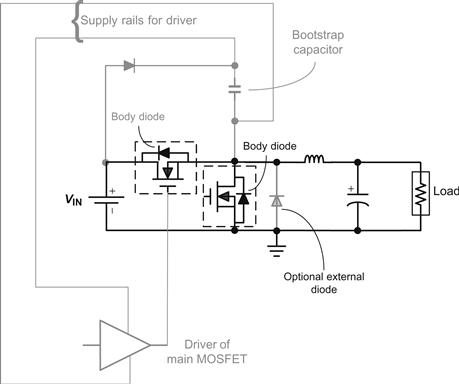
Figure 4.3: Synchronous Buck regulator with bootstrap circuit.
In “low-side current sensing,” to save the expense of a separate low-resistance sense resistor, the RDS of the “low-side MOSFET” (the one across the “optional” diode in Figure 4.3) is often used for sensing the current. The voltage drop across this MOSFET is measured, and so if we know its RDS, the current through it is also known by Ohm’s law. It becomes obvious that in fact for any low-side current sense technique, we need to turn the high-side MOSFET OFF, and thereby force the inductor current into the freewheeling path, so we can measure the current therein. That means we need to set the maximum duty cycle to less than 100%.
Another reason for choosing DMAX<100% comes from the use of N-channel MOSFETs in any (positive-to-positive) Buck regulators. Unlike an NPN transistor, an N-channel MOSFET’s Gate terminal has to be taken several volts above its Source terminal to turn it ON fully. So, to keep the switch ON, when the MOSFET conducts, we need to drive its Gate a few volts higher than the input rail. But such a rail is not available! The only way out is to create such a rail — by means of a circuit that can pump the input rail higher as required. This circuit is called the “bootstrap circuit,” as shown in Figure 4.3.
But to work, the bootstrap circuit demands we turn the switch OFF momentarily, because that is when the switching node goes low and the “bootstrap capacitor” gets charged up to VIN. Later, when the switch turns ON, the switching node (lower terminal of the bootstrap capacitor) rises up to VIN, and in the process, literally “drags” the upper terminal of the bootstrap capacitor to a voltage higher than VIN (by an amount equal to VIN as per the simplified bootstrap scheme of Figure 4.3) — that happens because no capacitor loses its charge spontaneously! Therefore, the reason for setting the maximum duty cycle to less than 100% is simply to allow a bootstrap circuit (if present) to work!
We will find that a bootstrap circuit is almost always present if an N-channel MOSFET switch is used in a positive-to-positive (or just “positive”) Buck converter, or in a positive-to-negative Buck-Boost, or in a negative-to-negative (or just “negative”) Boost. Further, by circuit symmetry we can show that it will also be required (though this time to create a drive rail below ground) when using a P-channel MOSFET in a negative Buck, or in a negative-to-positive Buck-Boost, or in a positive Boost. See Figure 9.16.
Here, we should also keep in mind that the N-channel MOSFET is probably the most popular choice for switches, since it is more cost-effective as compared to P-channel MOSFETs with comparable Drain-to-Source on-resistance “RDS.” That is because N-channel devices require smaller die sizes (and packages). Since we also know that the ubiquitous positive Buck topology requires a bootstrap circuit when using an N-channel MOSFET switch, it becomes apparent why a good majority of Buck ICs out there have maximum duty cycles of less than 100%.
Question 36: Why are Boost and Buck-Boost ICs almost invariably designed not to have 100% duty cycle?
Answer: We should first be clear that the Boost and Buck-Boost topologies are so similar in nature, that any IC meant for a Boost topology can also be used for a Buck-Boost application, and vice versa. Therefore, such control ICs are generally marketed as being for both Boost and Buck-Boost applications.
One of the common aspects of these two topologies is that in both of these, energy is built up in the inductor during the switch on-time, during which none passes to the output. Energy is delivered to the load only when the switch turns OFF. In other words, we have to turn the switch OFF to get any energy at all delivered to the output. Contrast this with a Buck, in which the inductor, being in series with the load, delivers energy to the load even as it is being built up in the inductor itself (during the switch on-time). So, in a Buck, even if we have 100% duty cycle (i.e., switch is ON for a long time), we will get the output voltage to rise (smoothly). Subsequently, the feedback loop will command the duty cycle to steady out when the required output voltage is reached.
However, in the Boost and Buck-Boost topologies, if we keep the switch ON permanently, we can never get the output to rise, because in these topologies, energy is delivered to the output only when the switch turns OFF. We can thus easily get into a “Catch 22” situation, where the controller “thinks” it is not doing enough to get the output to rise — and therefore continues to command maximum duty cycle. But with a maximum 100% duty cycle, that means zero off-time — so how can the output ever rise?! We can get trapped in this illogical mode for a long time, and the switch can be destroyed. Of course, we hope that the current limit circuit is designed well enough to eventually intervene, and turn the switch OFF before the switch destructs! But generally, it is considered inadvisable to run these two topologies at 100% duty cycle. The only known D=100% Buck-Boost IC is the LM3478 from National. Around since 2000, it still “sells” without a declaration of the problem.
Question 37: What are the “Primary” and “Secondary” sides of an off-line power supply?
Answer: Usually, the control IC drives the switch directly. Therefore, the IC must be located at the input side of the isolation transformer — that is called the “Primary side”. The transformer windings that go to the output are therefore said to all lie on the “Secondary side.” Between these Primary and Secondary sides lies “no-man’s land” — the “isolation boundary.” Safety norms regulate how strong or effective this boundary must be.
Question 38: In many off-line power supplies, we can see not one, but two optocouplers, usually sitting next to each other. Why?
Answer: The first optocoupler transmits error information from the output (Secondary side) to the control IC (Primary side). This closes the feedback loop, and tells the IC how much correction is required to regulate the output. This optocoupler is therefore often nicknamed the “regulation opto” or the “error opto.” However, safety regulations for off-line power supplies also demand that no “single-point failure” anywhere in the power supply produces a hazardous voltage on the output terminals. So if, for example, a critical component (or even a solder connection) within the normal feedback path fails, there would be no control left on the output, which could then rise to dangerous levels. To prevent this from happening, an independent “overvoltage protection” (OVP) circuit is almost invariably required. This is usually tied to the output rail in parallel to the components of the regulation circuitry. This fault detector circuit also needs to send its sensed “fault signal” to the IC through a separate path altogether, so that its functioning is not compromised in the event of failure of the feedback loop. So logically, we require an independent optocoupler — the “fault opto.” Note that by the same logic, this optocoupler must eventually connect to the IC (and cause it to shut down) using a pin other than the one being used for feedback. Early designs unknowingly thwarted this logic, and inadvertently got approved too by safety agencies too! Not any more though.
The reason why the two optocouplers are “sitting next to each other” is usually only for convenience in the PCB layout — because the isolation boundary needs to pass through these devices, and also through the transformer (see Figure 1.1 in Chapter 1).
Question 39: To get safety approvals in multioutput off-line converters, do we need separate current limiting on each output?
Answer: Safety agencies regulate not only the voltage at user-accessible outputs, but also the maximum energy that can be drawn from them under a fault condition. Primary-side current sensing can certainly limit the total energy delivered by the supply, but cannot limit the energy (or power) from each output individually. So for example, a 300 W converter (with appropriate primary-side current limiting) may have been originally designed for 5 V at the rate of 36 A and 12 V at the rate of 10 A. But what prevents us from trying to draw 25 A from the 12 V output alone (none from the 5 V)? To avoid running into problems like this during approvals, it is wise to design separate Secondary-side current-limiting circuits for each output. We are allowed to make an exception if we are using an integrated post-regulator (like the LM7805) on a given output, because such regulators have built-in current limiting. Note that any overcurrent fault signal can be “OR-ed” with the OVP signal, and communicated to the IC via the fault optocoupler.
Question 40: How do safety agencies typically test for single-point failures in off-line power supplies?
Answer: Any component can be shorted or opened by the safety agency during their testing. Even the possibility of a solder connection coming undone anywhere, or a bad “via” between layers of a PCB would be taken into account. Any such single-point failure is expected to usually cause the power supply to simply shut down gracefully, or even fail catastrophically. That is fine, but in the process, no hazardous voltage is permitted to appear on the outputs, even for a moment. And no fire hazard too!
Question 41: What is a synchronous Buck topology?
Answer: In synchronous topologies, the freewheeling diode of the conventional Buck topology is either replaced, or supplemented (in parallel) with an additional MOSFET switch (see Figure 4.3). This new MOSFET is called the “low-side MOSFET” or the “synchronous MOSFET,” and the upper MOSFET is now identified as being the “high-side MOSFET” or the “control MOSFET.”
In steady state, the low-side MOSFET is driven such that it is “inverted” or “complementary” with respect to the high-side MOSFET. This means that whenever one of these switches is ON, the other is OFF, and vice versa — that is why this is called “synchronous” as opposed to “synchronized” which would imply both are running in phase (which is clearly unacceptable because that would constitute a dead short across the input). However, through all this, the effective switch of the switching topology still remains the high-side MOSFET. It is the one that effectively “leads” — dictating when to build up energy in the inductor, and when to force the inductor current to start freewheeling. The low-side MOSFET basically just follows.
The essential difference from a conventional Buck regulator is that the low-side MOSFET in a synchronous regulator is designed to present a typical forward drop of only around 0.1 V or less to the freewheeling current, as compared to a Schottky catch diode which has a typical drop of around 0.5 V. This therefore reduces the conduction loss (in the freewheeling path) and enhances efficiency.
In principle, the low-side MOSFET does not have any significant crossover loss because there is virtually no overlap between its V and I waveforms — it switches (changes state) only when the voltage across it is almost zero. Therefore, typically, the high-side MOSFET is selected primarily on the basis of its high switching speed (low crossover loss), whereas the low-side MOSFET is chosen primarily on the basis of its low Drain-to-Source on-resistance, “RDS” (low conduction loss).
One of the most notable features of the synchronous Buck topology is that on decreasing the load, it typically does not enter discontinuous conduction mode as a diode-based (conventional) regulator would. That is because, unlike a bipolar junction transistor (BJT), the current can reverse its direction in a MOSFET (i.e., it can flow from Drain to Source or from Source to Drain). So, the inductor current at any given moment can become negative (flowing away from the load) — and therefore “continuous conduction mode” (CCM) is maintained — even if the load current drops to zero (nothing connected across the output terminals of the converter) (see Chapter 1). See also Chapter 9 and Figure 9.1.
Question 42: In synchronous Buck regulators, why do we sometimes use a Schottky diode in parallel to the low-side MOSFET, and sometimes we don’t?
Answer: We indicated above that the low-side switch is deliberately driven in such a manner that it changes its state only when the voltage across it is very small. That simply implies that during turn-off (of the high-side MOSFET), the low-side MOSFET turns ON a few nanoseconds later. And during turn-ON, the low-side MOSFET turns OFF just a little before the high-side MOSFET starts to conduct. By doing this, we are trying to achieve “zero-voltage (lossless) switching” (ZVS) in the low-side MOSFET. We are also trying to prevent “cross-conduction” — in which both MOSFETs may conduct simultaneously for a short interval during the transition (which can cause a loss of efficiency at best, and possible switch destruction too). However, during this brief interval when both MOSFETs are simultaneously OFF (the “dead-time”), the inductor current still needs a path to follow. However, every MOSFET contains an intrinsic “body diode” within its structure that allows reverse current to pass through it even if we haven’t turned it ON (see Figure 4.3). So, this provides the necessary path for the inductor current. However, the body diode has a basic problem — it is a “bad diode.” It does not switch fast, nor does it have a low forward drop. So often, for the sake of a couple of percentage points in improved efficiency, we may prefer not to depend on it, and use a “proper” diode (usually Schottky), strapped across the low-side MOSFET in particular. See Chapter 9.
Question 43: Why do most synchronous Buck regulators use a low-side MOSFET with an integrated Schottky diode?
Answer: In theory, we could just select a Schottky diode and solder it directly across the low-side MOSFET. But despite being physically present on the board, this diode may be serving no purpose at all! For example, to get the diode to take over the freewheeling current quickly from the low-side MOSFET when the latter turns OFF requires a good low-inductance connection between the two. Otherwise, the current may still prefer the body diode — for the critical few nanoseconds it takes before the high-side MOSFET turns ON. So, this requires we pay great attention to the PCB layout. But unfortunately, even our best efforts in that direction may not be enough — because of the significant inductive impedance that even small PCB trace lengths and internal bond wires of the devices can present when we are talking about nanoseconds. The way out of this is to use a low-side MOSFET with an integrated Schottky diode; that is, within the same package as the MOSFET. This greatly reduces the parasitic inductances between the low-side MOSFET and the diode, and allows the current to quickly steer away from the low-side MOSFET and into the parallel diode during the dead-time preceding the high-side turn-on.
Question 44: What limits our ability to switch a MOSFET fast?
Answer: When talking about a switching device (transistor), as opposed to a converter, the time it spends in transit between states is referred to as its “switching speed.” The ability to switch fast has several implications, including the obvious minimization of the V–I crossover losses. Modern MOSFETs, though considered very “fast” in comparison to BJTs, nevertheless do not respond instantly when their drivers change state. That is because, first, the driver itself has a certain non-zero “pull-up” or “pull-down” resistance through which the drive current must flow and thereby charge/discharge the internal parasitic capacitances of the MOSFET, so as to cause it to change state. In the process, there is a certain delay involved. Second, even if our external resistances were zero, there still remain parasitic inductances associated with the PCB traces leading up from the Gate drivers to the Gates, that will also limit our ability to force a large Gate current to turn the device ON or OFF quickly. And further, hypothetically, even if we do achieve zero external impedance in the Gate section, there remain internal impedances within the package of the MOSFET itself — before we can access its parasitic capacitances (to charge or discharge them as desired). Part of this internal impedance is inductive, consisting of the bond wires leading from the pin to the die, and part of it is resistive. The latter could be of the order of several ohms in fact. All these factors come into play in determining the switching speed of the device, thereby imposing hard limits as to what transition speeds are achievable.
Question 45: What is “cross-conduction” in a synchronous stage?
Answer: Since a MOSFET has a slight delay before it responds to its driver stage, though the square-wave driving signals to the high- and low-side MOSFETs might have no intended “overlap,” in reality the MOSFETs might actually be conducting simultaneously for a short duration. That is called “cross-conduction” or “shoot-through.” Even if minimized, it is enough to impair overall efficiency by several percentage points since it creates a short across the input terminals (limited only by various intervening parasitics).
This situation is aggravated if the two MOSFETs have significant “mismatch” in their switching speeds. In fact, usually, the low-side MOSFET is far more “sluggish” than the high-side MOSFET. That is because the low-side MOSFET is chosen primarily for its low forward resistance, “RDS·” But to achieve a low RDS, a larger die-size is required, and this usually leads to higher internal parasitic capacitances, which end up limiting the switching speed.
Question 46: How can we try to avoid cross-conduction in a synchronous stage?
Answer: To avoid cross-conduction, a deliberate delay needs to be introduced between one MOSFET turning ON and the other turning OFF. This is called the converter’s or controller’s “dead-time.” Note that during this time, freewheeling current is maintained via the diode present across the low-side MOSFET (or the Schottky diode in parallel).
Question 47: What is “adaptive dead-time”?
Answer: Techniques for implementing dead-time have evolved quite rapidly as outlined below.
• First Generation (Fixed Delay) — The first synchronous IC controllers had a fixed delay between the two Gate drivers. This had the advantage of simplicity, but the set delay time had to be made long enough to cover the many possible applications of the part, and also to accommodate a wide range of possible MOSFET choices by customers. The set delay had often to be further offset (made bigger) because of the rather wide manufacturing variations in its own value. However, whenever current is made to flow through the diode rather than the low-side MOSFET, we incur higher conduction losses. These are clearly proportional to the amount of dead-time, so we don’t want to set too large a fixed dead-time for all applications.
• Second Generation (Adaptive Delay) — Usually this is implemented as follows. The Gate voltage of the low-side MOSFET is monitored, to decide when to turn the high-side MOSFET ON. When this voltage goes below a certain threshold, it is assumed that the low-side MOSFET is OFF (a few nanoseconds of additional fixed delay may be included at this point), and then the high-side Gate is driven high. To decide when to turn the low-side MOSFET ON, we usually monitor the switching node in “real-time” and adapt to it. The reason for that is that after the high-side MOSFET turns OFF, the switching node starts falling (in an effort to allow the low-side to take over the inductor current). Unfortunately, the rate at which it falls is not very predictable, as it depends on various undefined parasitics, and also the application conditions. Further, we also want to implement something close to zero-voltage switching, to minimize crossover losses in the low-side MOSFET. Therefore, we need to wait a varying amount of time, until we have ascertained that the switching node has fallen below the threshold (before turning the low-side MOSFET ON). So, the adaptive technique allows “on-the-fly” delay adjustment for different MOSFETs and applications.
• Third Generation (Predictive Gate Drive™ Technique) — The whole purpose of adaptive switching is to intelligently switch with a delay just large enough to avoid significant cross-conduction and small enough so that the body-diode conduction time is minimized — and to be able to do that consistently, with a wide variety of MOSFETs. The “predictive” technique, introduced by Texas Instruments, is often seen by their competitors as “overkill.” But for the sake of completeness it is mentioned here. Predictive Gate Drive™ technology samples and holds information from the previous switching cycle to “predict” the minimum delay time for the next cycle. It works on the premise that the delay time required for the next switching cycle will be close to the requirements of the previous cycle. By using a digital control feedback system to detect body-diode conduction, this technology produces the precise timing signals necessary to operate very near the threshold of cross-conduction.
Question 48: What is low-side current sensing?
Answer: Historically, current sensing was most often done during the on-time of the switch. But nowadays, especially for synchronous Buck regulators in very efficient and/or very low-output voltage applications, the current is being sensed during the off-time.
For example, a rather extreme down-conversion ratio is being required nowadays — say 28–1 V at a minimum switching frequency of 300 kHz. We can calculate that this requires a duty cycle of 1/28=3.6%. At 300 kHz, the time period is 3.3 µs, and so the required (high-side) switch on-time is about 3.6×3.3/100=0.12 μS (i.e., 120 ns). At 600 kHz, this on-time falls to 60 ns, and at 1.2 MHz it is 30 ns. Ultimately, that just may not give enough time to turn ON the high-side MOSFET fully, “de-glitch” the noise associated with its turn-on transition (“leading edge blanking”), and get the current limit circuit to sense the current fast enough.
Further, at very light loads we may want to be able to skip pulses altogether, so as to maximize efficiency (since switching losses go down whenever we skip pulses). We don’t want to be forced into turning the high-side MOSFET ON every cycle — just to sense the current!
For such reasons, low-side current sensing is becoming increasingly popular. Sometimes, a current sense resistor may be placed in the freewheeling path for the purpose, or the forward drop across the low-side MOSFET is often used for the purpose. For “DCR sensing,” see Figure 9.6.
Question 49: Why do some non-synchronous regulators go into an almost chaotic switching mode at very light loads?
Answer: As we decrease the load, conventional regulators operating in continuous conduction mode (CCM— see Figure 1.9) enter discontinuous conduction mode (DCM). The onset of this is indicated by the fact that the duty cycle suddenly becomes a function of load — unlike a regulator operating in CCM, in which the duty cycle depends only on the input and output voltages (to a first order). As the load current is decreased further, the DCM duty cycle keeps decreasing, and eventually, many regulators will automatically enter a random pulse-skipping mode. That happens simply because at some point, the regulator just cannot decrease its on-time further, as is being demanded. So, the energy it thereby puts out into the inductor every on-pulse starts exceeding the average energy (per pulse) requirement of the load. So, its control section literally “gets confused,” but nevertheless tries valiantly to regulate by stating something like — “oops … that pulse was too wide (sorry, just couldn’t help it), but let me cut back on delivering any pulses altogether for some time — hope to compensate for my actions.”
But this chaotic control can pose a practical problem, especially when dealing with current-mode control (CMC). In CMC, usually the switch current is constantly monitored, and that information is used to produce the internal ramp for the pulse-width modulator (PWM) stage to work. So, if the switch does not even turn ON for several cycles, there is no ramp either for the PWM to work off.
This chaotic mode is also a variable frequency mode of virtually unpredictable frequency spectrum and therefore unpredictable EMI and noise characteristics too. That is why fixed-frequency operation is usually preferred in commercial applications. And fixed frequency basically means no pulse-skipping!
The popular way to avoid this chaotic mode is to “pre-load” the converter, that is, place some resistors across its output terminals (on the PCB itself), so that the converter “thinks” there is some minimum load always present. In other words, we demand a little more energy than the minimum energy that the converter can deliver (before going chaotic).
Question 50: Why do we sometimes want to skip pulses at light loads?
Answer: In some applications, especially battery-powered applications, the “light-load efficiency” of a converter is of great concern. Conduction losses can always be decreased by using switches with low forward drops. Unfortunately, switching losses occur every time we actually switch. So, the only way to reduce them is by not switching, if that is possible. A pulse-skipping architecture, if properly implemented, will clearly improve the light-load efficiency.
Question 51: How can we implement controlled pulse-skipping in a synchronous Buck topology, to further improve the efficiency at light loads?
Answer: In DCM, the duty cycle is a function of the load current. So, on decreasing the load sufficiently, the duty cycle starts to “pinch off” (from its CCM value). And this eventually leads to pulse-skipping when the control runs into its minimum on-time limit. But as mentioned, this skip mode can be fairly chaotic, and also occurs only at extremely light loads. So, one of the ways this is being handled nowadays is to not “allow” the DCM duty cycle to pinch off below 85% of the CCM pulse width. Therefore, now more energy is pushed out into a single on-pulse than under normal DCM — and without waiting to run into the minimum on-time limits of the controller. However, now because of the much-bigger-than-required on-pulse, the control will skip even more cycles (for every on-pulse). Thereafter, at some point, the control will detect that the output voltage has fallen too much, and will command another big on-pulse. So, this forces pulse-skipping in DCM, and thereby enhances the light-load efficiency by reducing the switching losses.
Question 52: How can we quickly damage a Boost regulator?
Answer: The problem with a Boost regulator is that as soon as we apply input power, a huge inrush current flows to charge up the output capacitor. Since the switch is not in series with it, we have no control over it either. So ideally, we should delay turning ON our switch until the output capacitor has reached the level of the input voltage (inrush stops). And for this, a soft-start function is highly desirable in a Boost. However, if while the inrush is still in progress, we turn the switch ON, it will start diverting this inrush into the switch. The problem with that is in most controllers, the current limit may not even be working for the first 100 ns to 200 ns after turn-on — that being deliberately done to avoid falsely triggering ON the noise generated during the switch transition (“leading edge blanking”). Now the huge inrush current gets fully diverted into the switch, with virtually no control, possibly causing failure. One way out of that is to use a diode directly connected between the input supply rail and the output capacitor (cathode of this diode being at the positive terminal of the output capacitor). So, the inrush current bypasses the inductor and Boost diode altogether. However, we have to be careful about the surge current rating of this extra diode. It need not be a fast diode, since it “goes out of the picture” as soon as we start switching (gets reverse-biased permanently).
Note also, that a proper ON/OFF function cannot be implemented on a Boost topology (as is). For that, an additional series transistor is required, to completely and effectively disconnect the output from the input. Otherwise, even if we keep the switch OFF permanently, the output rail will rise to the input level.
This FAQ was presented in an early chapter so as to not intimidate an entry-level person. For the experienced user, much more on synchronous and other topologies, plus several modern techniques is available in Chapter 9. Also refer to the solved examples in Chapter 19 to seal concepts and perform design calculations.