
Chapter 17
Fixing EMI Across the Board and Input Filter Instability
This chapter is a broad sweep of the most practical ways of EMI mitigation on the board. The ground plane, the flux band, cancellation windings, beads, and so on are all covered. Filters for dc–dc converters (modules) are also discussed, and the phenomenon of input instability, based on Middlebrook’s extra-element theorem, is mathematically and graphically analyzed in a very simplified manner.
Part 1: Practical Techniques for EMI Mitigation
Here we first look at some of the practical design aspects involved in controlling EMI. These supplement the basic PCB layout guidelines presented in Chapter 10. We first emphasize one aspect of that chapter: that the most potent and cost-effective method of reducing EMI is the ground plane.
The Ground Plane
The ground plane is a very effective method of bringing down the overall level of the EMI emissions. On a multilayer board, if the very next layer to the side containing the power components (and their associated traces) is this ground plane, the EMI can drop by about 10–20 dB. This is more cost-effective than opting initially for a “cheap” one- or two-sided board, and then having to use bulky filters later. However, the integrity of a ground plane should be maintained, as far as possible.
We should remember that return currents tend to travel by the shortest straight line path at low frequencies. But at high frequencies (or the higher harmonics of the switching waveform), the return currents tend to image themselves directly under their respective forward traces (on the opposite layer). Therefore, currents, given a chance, automatically try to reduce the area they enclose — as this lowers the self-inductance, and thereby offers the current, the lowest impedance route possible (at low frequencies, trace impedances are resistive, but at high frequencies they are inductive). So, for example, if we make ill-considered cuts in the ground plane (possibly with the intention of “conveniently” routing some other trace), the return currents of the power converter stage will get diverted along the sides of any intervening cuts, and will thereby effectively create slot antennas on the PCB.
The Role of the Transformer in EMI
Very often a young engineer resolves a stubborn EMI problem by just “playing” with the transformer. We can learn a lot from similar excursions. With magnetics in general, nothing is perhaps completely known or obvious.
The transformer comes into the picture in the following ways:
• With its windings carrying high-frequency current, it becomes an effective H-field antenna. These fields can impinge upon nearby traces and cables, and enlist their help in getting transported out of the enclosure, via conduction or radiation.
• Since parts of the windings have a swinging voltage across them, they can also become effective E-field antennas.
• The parasitic capacitance between the Primary and Secondary windings transfers noise across the isolation boundary. Since the Secondary-side ground is usually connected to the chassis, this noise returns via the Earth plane, in the form of CM noise. The situation is very similar to the tradeoffs required in heatsink mounting issues. In this case, we wish to couple the Primary and Secondary very close to each other in order to reduce leakage inductance (especially in flyback transformers), but this also increases their mutual capacitance, and thus the CM noise.
Here are some standard techniques that help prevent the above:
• In a safety-approved transformer, there are three layers of safety-approved polyester (“Mylar®”) tape between the Primary and Secondary windings, for example, the popular #1298 from 3M. In addition to these layers, a copper “Faraday shield” may be inserted to “collect” the noise currents arriving at the isolation boundary, and divert them (usually to the Primary ground) (see Figure 17.1). Note that this shield should be a very thin strip of copper foil so as to avoid eddy current losses and also keep the leakage inductance down. So, it is typically 2–4 mils thick, consisting of one turn wound around the center limb. A wire is soldered close to its approximate geometric center and goes to the Primary ground. Note that the ends of the copper shield should not be galvanically connected together, as that would constitute a shorted turn from the viewpoint of the transformer. Some designs also use another Faraday shield, on the Secondary side (after the three layers of insulation). This is connected to the Secondary ground. However, most commercial ITE (information technology equipment) power supplies don’t need either of these shields, provided adequate thought has gone into the winding and construction, as we will soon see.
• There is usually also a circumferential copper shield (or “flux band”) around the entire transformer (see Figure 17.1). The ends of this shield can be, and are usually, shorted (soldered) together. It serves primarily as a radiation shield. It is often left floating in low-cost designs. However, it may (and should) be connected to the Secondary ground. Safety issues will need to be considered, in regards to IEC 60950-1 requirements in terms of insulation between Primary and Secondary and separations (the required Primary to Secondary “creepage,” i.e., distance along the insulating surfaces, and “clearance,” i.e., shortest distance through air) as applicable. When the transformer uses an air gap on its outer limbs, the fringing flux emanating from the gap causes eddy current losses in the band. So, this band is also usually only 2–4 mils thick. Like the Faraday shield, this too can often be omitted by good winding techniques.
• To reiterate, from the point of view of EMI, a flyback transformer should be preferably center-gapped, that is, no gap on its outer limbs. The fringing fields from exposed air gaps become strong sources of radiated EMI besides causing significant eddy current losses in the surrounding copper band.
• There is usually an auxiliary winding present on the Primary side, which provides a low-voltage rail for the controller and related circuitry. One end of this is connected to Primary ground. Therefore, it can actually double over as a crude Faraday shield if we (a) wind it evenly and spread it out over the available bobbin width and (b) help it collect and divert noise by AC-coupling its opposite end (i.e., the diode end) to Primary ground, through a small 22- to 100-pF ceramic capacitor as shown in the topmost schematic of Figure 17.2.
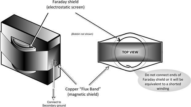
Figure 17.1: Screens used for transformers.
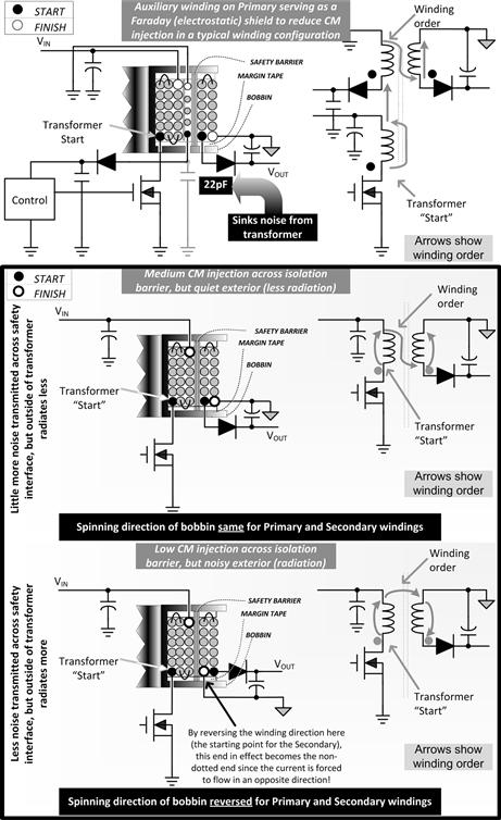
Figure 17.2: Low-noise transformer winding techniques.
Figure 17.2 also reveals low-noise construction techniques as applied to a typical flyback transformer. We should compare the right-hand schematics with their equivalent “winding” versions on the left. In the discussion below, we note that though transformers with split windings are not being explicitly discussed here, the same principles can be easily extended and applied to them too. Here are some observations based on Figure 17.2:
• Since the Drain of the FET is swinging, it is a good idea to keep the corresponding end of the Primary winding buried as deep as possible, that is, it should be the first layer to be wound on the bobbin. The outer layers tend to shield the fields emanating from the layers below. For sure, the Drain end of this winding should not be adjacent to the “safety barrier” (the three layers of polyester tape) because the injected noise current is proportional to the net dV/dt across the two “plates” of the parasitic capacitor (formed by the windings on either side of the interface). Since we really cannot reduce the capacitance much (without adversely impacting the leakage inductance), we should at least try to reduce the net dV/dt across this interface capacitor.
• Comparing any diagram on the left with its corresponding schematic on the right, we see that the “start” and “finish” ends of any winding have also been indicated. In particular, all the start ends have been shown with dots in the schematic. Note that in a typical production sequence, the coil winding machine always spins the bobbin in the same direction, for every layer and winding placed successively. Therefore, since all the start ends (i.e., dotted ends) are magnetically equivalent, if one dotted end goes high, the other dots also go high at the same moment (as compared to their opposite ends). We can also see that from the point of view of the actual physical proximities involved, every dotted end of a winding automatically falls close to the nondotted end of the next winding (with the usual fixed winding direction). This means that for the flyback transformer of Figure 17.2, the diode end of the Secondary winding will then necessarily fall adjacent to the safety barrier. Yes, because of that we will have a certain amount of dV/dt still present across the barrier. But note that this dV/dt is much smaller than if the Drain end of the Primary winding was brought adjacent to the safety barrier (because of the bigger voltage swing on the Primary side, due to the large turns ratio). However, the transformer as shown in the top two schematics of Figure 17.2 now has the advantage that the “quiet end” (ground) of the Secondary winding is now the outermost layer. That is by itself a good shield. So, we can safely drop the ubiquitous circumferential shield (flux band). Consider the alternative — suppose we had wound the transformer the “wrong” way, that is, by reversing all the start and finish ends shown in Figure 17.2. That would have brought the Drain end of the Primary winding right next to the safety barrier, with the Secondary ground end (which is usually connected to the chassis) directly across the isolation boundary. With this winding arrangement, we would have a healthy dose of CM noise injected directly into the chassis/Earth — not the best way to achieve compliance for sure.
• When we go through the same reasoning for a Forward converter transformer, we will find that with the described winding sequence, we will automatically have the quiet ends of both Primary and Secondary windings “overlooking each other” across the safety barrier (isolation boundary). That is because the relative polarities between the Primary and Secondary windings in a Forward converter are opposite to those of a flyback transformer. So now, very little noise will be injected through the parasitic capacitance. That is good. But the outermost layer is not “quiet” anymore, and we could have a radiation problem. So, in this case, the circumferential shield may become necessary.
• Another way out of the Forward converter “outer surface radiation problem” is to ask our production team to reverse the direction of the Secondary winding (only). So, for example, if up to the finish of the Primary winding, the machine was spinning clockwise, for the Secondary we should specify an anticlockwise direction (with expected resistance coming, not from the transformer, but our production staff!). If we do that, the reasoning given previously for the flyback will now apply unchanged to the Forward converter transformer too. So, we would now have a “quiet” exterior (without any flux band necessary), though some more common-mode noise will be transferred across the isolation boundary due to the dV/dt. Note that in general, aiming for a “quiet” exterior (low radiation) seems to be a better option than trying solely to prevent noise injection through the interface capacitance, because the latter can be overcome by various tricks — like having the auxiliary winding double over as a Faraday shield, and so on. But a radiation problem can be hard to manage. We do note, however, that a Forward converter transformer has no (or very small) air gap, so it is generally considered “quieter” in terms of radiation to start with (as compared to a flyback).
• In the lowermost schematic of Figure 17.2, we have an alternative winding technique for those flyback cases where we are troubled by conducted EMI noise, in particular CM noise. The way to minimize that is to then reduce the dV/dt across the safety barrier, by bringing the quiet end of the Secondary winding next to the safety interface.
Tip: We don’t need to draw any current at all from the “Faraday winding” (uppermost schematic of Figure 17.2) to make it work. So, it need not even be required by our circuitry (for an auxiliary power rail). In that case, we could just wrap a few turns of thin wire (spread out evenly), with one end of it connected to Primary ground and the other end via a small 22-pF capacitor to Primary ground. This technique certainly saves production costs associated with the making and placing of a formal Faraday shield — not to mention the improvement in efficiency due to the reduced leakage inductance (as compared to what a formal Faraday shield may lead to). In that sense, this informal Faraday shield is a very useful idea, worth trying out.
• When the transistor is mounted on the chassis for thermal reasons, there is a technique that is used to actually try to cancel the current injected through the heatsink capacitance. This is done by placing another winding, equivalent to the main winding, and opposite in phase — when one winding turns OFF, this noise recovery winding turns ON. Note that the noise recovery winding can be of much thinner wire (see Figure 17.3). The idea is that if the noise current (Icmx) is being pushed out from the Primary winding, the cancellation winding gets the same current pulled in. Therefore, in effect, the injected current does a quick “U-turn” back to its noise source. Note that this additional cancellation winding should be very closely coupled to the main winding. Often it is wound bifilar with the Primary winding (i.e., both wound simultaneously, rather than one on top of the other). However, we should be aware that in that case, we will have a high-voltage differential between the two windings at points along their length. So if, for example, there are pinholes in the enamel insulation, there is a danger of flashover and resulting failure of the power supply. The solution is to use wires with “double insulation.” In Figure 17.3, the cancellation winding method is shown along with another technique we had presented in Figure 16.4. Both are independent, and either one, or both, can be used for good results.
Note: The above technique does nothing to cancel the noise injected through the interface capacitance (i.e., between the Primary and Secondary windings). But despite that limitation, a 5–10-dB μV reduction in conducted EMI is still possible (at various points in the EMI spectrum). So, this could certainly be worth trying out, if there is a last-minute problem and a major redesign of the board needs to be avoided. It may be therefore prudent to plan for this winding in advance, including a PCB placeholder for the additional Y-capacitor.
Note: The above idea can clearly be applied to any off-line topology (and also all high-power DC–DC converters) — whenever the switch needs to be mounted on the chassis/enclosure (and its Drain is swinging). A similar technique may be useful on the Secondary side too, if the catch diode is to be mounted on the chassis. However, this Secondary-side heatsink noise injection is of concern only when the tab of the diode (which is almost invariably the cathode of the diode) happens to be the switching node for that particular topology/configuration. So, we can work out that the normal Boost and flyback topologies don’t have this problem, since the cathode end of their diodes is “quiet.” However, the (positive-to-positive) Buck and the Forward converter do have swinging cathodes (tabs), so we should be careful when chassis-mounting their diodes.
• Rod inductors are often used in LC post-filtering stages on the output. Because of their open magnetic structure, they have been called “EMI cannons.” But they are nevertheless still popular because of their low cost, and also the low “real estate” they need. Some tricks have therefore been developed to control their ill-effects. They should be placed vertically (as they normally are). Then, if two such rods are being used on a given output, we should wind the two rods identically, but reverse the current flow in one of them, as compared to the other (by suitable modification of the PCB) (see Figure 17.4). Looking from the top, one rod should be carrying current clockwise and the other anticlockwise. This helps redirect the flux from one, back into the other (“U-turn”). In that way, much less “EMI-spilling” occurs.
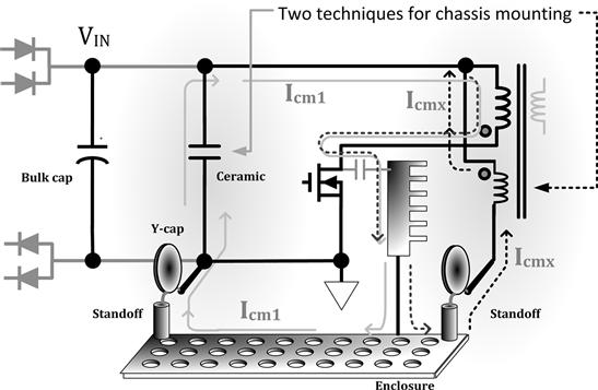
Figure 17.3: Cancellation winding to reduce CM noise and direct return method.
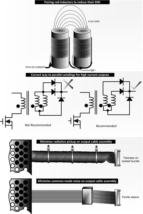
Figure 17.4: Ways to reduce EMI.
EMI from Diodes
Here we list some of the things to keep in mind and try out, as regards diodes:
• Diodes are a potent source of low- to high-frequency noise. Slow diodes (like those in a typical input bridge) can also contribute significant wideband noise.
• Input bridges which use ultrafast diodes are available, and their vendors claim significant reduction in EMI. But in practice they don’t seem to provide much advantage. They also typically have much lower input surge current ratings. In fact, in a front-end position, any component always needs to be able to handle a lot of stress (if not abuse), such as the inrush stresses occurring during power-up at high line.
• To minimize EMI, ultrafast diodes should be selected on the basis of softer reverse recovery characteristics. For medium- to high-power converters, RC snubbers are also often placed across these diodes (at the expense of some efficiency). In low-voltage applications, Schottky diodes are often used. Though these diodes have no reverse recovery time in principle, their body capacitance can be relatively high, and can end up resonating with PCB trace inductances. So an RC snubber is also often helpful for Schottkys. Note that if any diode has been fully recovered (i.e., zero current) before the voltage across it starts to swing, there is no reverse recovery current. In that case, diodes really don’t have to be “super-super-fast.” In fact, many engineers have reported much lower EMI by choosing slower diodes for snubbers/clamps. A popular choice for snubber applications is the soft-recovery fast diode BYV26C (or BYM26C for medium power) from NXP (formerly Philips).
• It is advisable to have the FET switch roughly two to three times slower than the reverse recovery time of the catch diode — to avoid shoot-through currents — which will produce strong H-fields (in addition to causing dissipation). Therefore, it is not uncommon to intentionally degrade the FET switching speed by adding a resistor (typically 10–100 Ω in off-line applications) in series with the Gate — maybe with a diode across the Gate resistor so as to leave the turn-off speed unaffected (for efficiency reasons).
• Small capacitors may often be placed across the FET (Drain-to-Source). But this can create a lot of dissipation inside the FET, since every cycle the capacitor energy is dumped into the switch.
• Ultrafast diodes also exhibit high forward-voltage spikes at turn-on. So momentarily, the diode forward voltage may be 5–10 V (rather than the expected 1 V or so). Usually, the snappier the reverse recovery, the worse is the forward spike too. Therefore, at FET turn-off, the diodes become strong E-field sources (voltage spikes), whereas at FET turn-on, the diodes will generate strong H-fields (current spikes). A small RC snubber across the diode will help control the forward-voltage spike.
• In integrated switchers, access to the Gate of the FET may not be available. In that case, the turn-on transition can be slowed by inserting a resistor of about 10–50 Ω in series with the bootstrap capacitor. The bootstrap capacitor is in effect the voltage source for the internal floating driver stage. At turn-on, it is asked to provide the high-current spike required to charge up the Gate capacitance of the FET. So, a resistor placed in series with this bootstrap capacitor limits the Gate charging current somewhat, and thereby slows the turn-on.
• To control EMI, ferrite beads (preferably of lossy nickel-zinc material) are sometimes placed in series with catch diodes (often slipped on to their leads), such as at the output diode of a typical off-line flyback. However, these beads must be very small, as they can have a significant effect on the efficiency of the power supply.
Note: In multi-output off-line flyback converters, we may find larger beads (possibly with more than one turn, and made of the more common manganese–zinc ferrite) in series with the output diodes belonging to some of the auxiliary outputs (i.e., those not being directly regulated). But the purpose of these beads is not EMI suppression, but to block some of the voltseconds and thereby improve the “centering” of the outputs.
• A comment about split/sandwich windings. In general, the Primary winding may be broken up into two windings, which are then positioned on either side of the Secondary winding — so as to reduce leakage inductance in flybacks, and proximity effect losses in Forward converters. This is acceptable for EMI provided the two-split winding sections are in series. In general, putting windings in parallel is not a good idea (especially from the EMI point of view). In high-current power supplies, the Secondary winding is also sometimes broken up into two windings (or foils). The intention is usually to increase the current handling capability (see Figure 17.5). But these split Secondaries are also usually placed physically apart, on either side of the Primary winding. However, in paralleled windings, the two supposedly “equal” sections are actually always magnetically slightly different — because of their different physical positions inside the transformer. Plus, their DCR is also just a little different (different lengths), creating the possibility of an internal current loop. The designer may be completely unaware of the current loop, except for severe tell-tale ringing present on the voltage waveform and a “mysteriously” bad EMI scan. There could also be a lot of unexpected heating. So, if paralleling is really needed, it is better to use the scheme shown in Figure 17.4 on the right-hand side. Here the forward drops of the two diodes help “ballast” the windings, and this also helps “iron out” any inequality between the two halves.
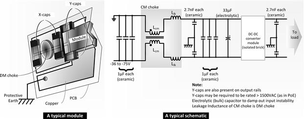
Figure 17.5: Typical EMI filter for DC–DC modules (Bricks).
Are We Going to Fail the Radiation Test?
Most of the smaller companies cannot afford a precompliance setup for radiated emission tests. However, a few of them have a fairly good idea beforehand, whether they are going to be successful in that test or not — just by looking hard at the conducted EMI scan. What they do is to carefully look at the spectrum in the third region of CISPR-22. This is the flat region from 5 MHz to 30 MHz. They can even scan higher to higher frequencies, if possible. They realize that even though they may have achieved compliance with the conducted limits in this third region, it is not good enough! So, they look at the overall shape of the plot in this region. If they find that it is gradually rising toward the 30-MHz end, they are quite confident that they have a radiation problem. However, if the plot starts drooping, or remains generally flat as 30 MHz approaches, they are likely to immediately submit the prototype to a lab for the formal radiated limit compliance certification. In other words, one can actually “see” the energy level in the 5–30-MHz region. If there is an unexpected amount of conducted noise energy in this region, radiation can’t be too far off either!
A quick diagnostic test for understanding a particular high-frequency-conducted EMI problem is to twist the output cables of the power supply tightly together (along with their respective return wires). This induces field cancellation (also called flux containment), thus reducing radiation effects related to the output cables (if present) (see Figure 17.4). If the conducted EMI scan really improves by twisting, we may have a radiation problem — either from the enclosure or the output cables themselves, or from both.
The above-described twisting procedure was actually implemented in full production on a particular high-volume commercial design. A few tie-wraps were used to hold the bunch of wires tightly together along the twisted position. This happened to be a last-ditch effort to avoid costly last-minute redesign just before full production. This “twist-and-tie-wrap” technique is admittedly not very practicable or desirable in production. But it is cheap. Note that a ferrite sleeve, slipped over the entire output cable bunch, was also found to be working well. But it was disqualified simply because it was far more expensive than three or four tie-wraps! However, it is interesting to note here that though a ferrite sleeve may look like a radiation shield and even produce almost similar results as twisting the cables, it actually works by reducing the common-mode noise currents themselves, not merely by “shielding” the EMI due to these tiny currents. Twisting, on the other hand, tries to cancel the fields of adjacent wires (with their returns). Looking back, in this particular case, the root cause was that there was obviously a significant amount of common-mode noise already present on the output, which was causing the output cables to radiate. The radiation was thereafter being picked up by the input cables, leading to a failed conducted EMI test.
Part 2: Modules and Input Instability
There are certain things we may do unintentionally at the input of the converter that can have a major impact on the performance of the EMI filter, and also the converter itself. If we don’t know the rules of the game, we can end up saturating our filter chokes and even inducing basic converter instability.
Practical Line Filters in DC–DC Converter Modules
See Figure 17.5c for an example of how EMI suppression techniques are applied to DC–DC converters. We have shown an industry standard isolated “brick” along with its external EMI filtering. The input to this particular module is a coarsely regulated “−48VDC” or “−60VDC” bus, forming part of a distributed power architecture for a data/telecom network. Its output is isolated and regulated (e.g., 3.3 V/50 A, 12 V/10 A, or 48 V/2 A, and so on). The −48VDC input is usually derived from an off-line telecom power supply (called a “rectifier”).
See how the traces are laid out in the module’s external EMI filter. Note, in particular, the placement of the Y-caps. We should also keep in mind that one of the most effective methods of suppressing EMI, especially in board-mounted DC–DC converters, is a good ground plane. On a multilayer board, best results are usually obtained by having this plane be the internal layer just below the top (power) component side. Up to 20-dB reduction in noise is possible.
Note: As per typical safety regulations, voltages below 60 VDC are generally considered non-hazardous and therefore not subject to the isolation/earthing requirements described earlier. The Y-caps on the output rail can be just 100-V standard caps or less. However, in distributed power networks, such as Power over Ethernet, we require 1,500-VAC isolation from the power cable network to the enclosure to protect the user from spikes picked up on the long cables. So, the Y-caps shown in the figure may be required to be (standard) 2-kV-rated components. However, since there is no AC, we are not governed by AC leakage safety restrictions. Therefore, very large Y-caps can be used if desired.
Note: For protection against ESD (electrostatic discharge) upsets, 0.01-μF caps between the terminal block contacts and Earth are often also included. These are essentially Y-caps. But note that there have been cases, particularly when these caps were ordinary 50-V multilayer ceramic (“MLCs”), which got destroyed during the course of an ESD test — simply because they got charged up to excessive voltages! Therefore, these capacitors, and any other Y-caps present, must be evaluated under abnormal but likely disturbances too. Eventually, we may need to increase the capacitance and/or the voltage rating and/or size of the caps just to protect them from/against overcharging.
Since around 1971 the phenomenon of “input oscillations” or “input instability” has received quite a lot of attention. It has been shown that instability can occur if the output impedance of the filter is not within a certain “safe” window, as related to the input impedance of the converter (we are talking about the impedances presented to the power flow now — not to the CM or DM noise). So, with the modern trend of low-impedance “all-ceramic” solutions in DC–DC converters, the possibility of this particular type of instability is becoming more and more real.
One of the easiest ways to see the impact of the negative input impedance of a typical converter is to set it up with only ceramic input capacitors (about 10 μF or less) — and then do a “hard power-up.” In this type of power-up test, the dV/dt of the applied input is kept intentionally very high. On the bench, this can be done by simply slamming the banana plug from the input of the converter into the output terminals of a (low-impedance/high-current) lab DC power supply. Then, if we monitor the input (supply) pin of the converter with a digital oscilloscope (triggered correctly, and in one-shot acquisition mode), we will see an initial overshoot — that can be as high as 1.5–2.5 times the supposed DC voltage level (as set on the lab supply). Note that if the input capacitance is large enough (beyond a certain value), the dV/dt (and overshoot) gets automatically reduced, due to the higher charging current required for this input capacitor. On the other hand, if the ceramic capacitor is replaced by an aluminum electrolytic (even with a lower capacitance), the overshoot is dramatically reduced. Tantalum capacitors also produce overshoots under hard power-up, but these are less pronounced than with ceramic.
Note: We should remember that in any case, it’s never a very good idea to use tantalums at the input of any converter — due to tantalum’s inherent surge current limitations. However, if for some reason, tantalums must be used at the input (in any topology), or at the outputs (for a Boost or Buck-Boost), we must ensure that they are “100% surge-tested” by their vendors. And even for such surge-tested tantalum capacitors, it is recommended that the maximum voltage applied across them in our application be less than half their voltage rating, that is, a voltage derating of 50%. This was also discussed in Chapter 6.
We see that it is possible to damage a DC–DC converter, which uses only small-value ceramic capacitors at its input — more so when we already happen to be operating rather close to its maximum input voltage rating.
The reader should note that in Figure 17.5, we have placed an electrolytic capacitor in parallel to the ceramic input capacitors — for the purpose of damping out “input instability.” This needs further explaining. To understand the underlying causes associated with this phenomenon, we need to start with the well-known Buck converter equations and see what happens if we (hypothetically) “jiggle” the duty cycle, just a little bit, around its steady-state value. Note that in a practical situation, this could happen very easily under normal line or load transients. Therefore, expressing the input voltage and the input current as a function of duty cycle, we get (for a Buck)
![]()
![]()
So,
![]()
Dividing the above equations, we get (for a Buck converter)
![]()
V/I, above, is resistance. It is the incremental resistance at the input. Let us call it “RIN.” So, for a Buck converter, the incremental resistance in ohms is
![]()
Here RL is the load resistance (ohms), and is assumed constant. Note that both the input voltage and the input current always have positive values in a (positive-to-positive) Buck converter. Therefore, the ratio VIN/IIN is also certainly a positive quantity. It’s only the relative change that is in opposite directions — hence the minus sign in the equation above. Mathematics aside, all this means is that since the input of a converter is a constant power input (PO≈PIN), if input voltage falls, the current increases, just the opposite of a pure resistance.
Example:
What is the input resistance of a 3.3-V/50-V brick, with an input range of 36–75 V?
Output power is 3.3×50=165 W. RL is 3.3/50=0.066 Ω. Duty cycle is 3.3/36=0.092 at 36-V input. So, RIN is −0.066/(0.092)2=−7.8 Ω. In terms of decibels, we get −20×log(7.8)≅−18 dB Ω (do not try to take log of a negative number!). A similar calculation at 75-V input gives −31 dB Ω. We will see that this means that input instability is more likely to occur at low input voltages.
What is it about the interaction of the impedances at the filter–converter interface that causes this instability? Let us see what is really happening as we jiggle the input to the filter (VIN) in Figure 17.6.
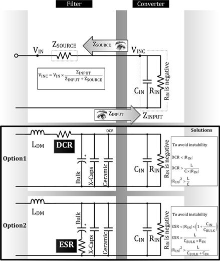
Figure 17.6: Input interaction and two possible solutions to increase damping.
VINC is the voltage that appears at the terminals of the converter. The filter impedance and the converter impedance form a voltage divider.
![]()
Using a regular voltage divider, there would be no problem. We use such a divider to set the voltage on the feedback pin of our controller. In that case, if we raise VIN, we expect VINC to rise too — provided both the resistors of the divider are “normal.” But in our case, one of them, ZINPUT, is not “normal” — it is a negative resistance. So what really happens is if we increase VIN, then VINC falls! The control loop of the converter will “think” that the input has fallen rather than increased, so it will respond incorrectly to the change. And isn’t that the usual recipe for output oscillations?
Note that above we are talking not about DC values, but changes (increments), that is, AC values. So, we can identify that the problem really starts when VINC is negative. Because a negative VINC simply means that VINC is moving in an opposite direction to VIN, confusing the feedback loop. Note that in the equation for VINC above, the numerator is already negative. So, the only way to get a positive sign for VINC is to make the denominator negative too. This means the basic criterion for avoiding input instability is
![]()
Now, in reality, the input impedance of the converter is frequency dependent (RIN was just the low-frequency value of ZINPUT). In the more detailed converter model, a parallel capacitance CIN (see Figure 17.6) appears across the input of the converter, mainly due to the output filter components of the converter being reflected into the input. This causes the downward slope in Figure 17.7. It increases the chance of input instability. In Figure 17.7, we have shown a typical input impedance plot with respect to frequency. Note that only the magnitude of the converter input impedance has been displayed, primarily because the y-axis is in log scale, and we know that log scales cannot be negative.
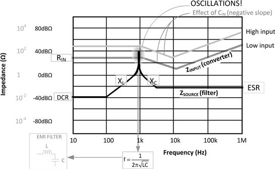
Figure 17.7: Input filter interaction and Middlebrook’s stability criterion explained.
ZSOURCE (the output impedance of the filter) is also changing with frequency. Looking into the output terminals of the filter (from converter), we see basically a simple parallel LC filter stage. Therefore, ZSOURCE has the shape indicated in Figure 17.7.
The stability criterion means that we are demanding that the output impedance of the filter must be always less than the input impedance of the converter for any frequency. But what happens if the LC filter has insufficient damping and therefore has a resonance peak? This is the oval highlighted problem area in Figure 17.7, and we can see that in this region we are violating the basic stability criterion. This resonant peak needs to be suppressed. Therefore, in addition to the basic stability criterion, a follow-up criterion must be added to ensure that at the LC corner frequency, the LC filter peak is properly damped out (Q=1). This applies to the EMI filter design procedures described in Chapter 18 too.
For ensuring damping, we could simply add some more resistance to the choke (DCR) as shown in Figure 17.6. But that is not a very good idea since the entire operating current also passes through this choke, and the overall efficiency would suffer. Instead, it is preferable to add a slight resistance (ESR) to the capacitor as also shown in Figure 17.6. We know that any capacitor in steady-state blocks any DC voltage completely. So, the input capacitor sees only the AC component of the input current flowing into the switching FET. This therefore correspondingly reduces the dissipation required to achieve a given target of damping. However, we also need to maintain good decoupling at the input of the converter (to keep its control sections from getting affected, as also to suppress EMI). Therefore, the usual commercially implemented solution for such bricks is to place an additional high-ESR capacitor in parallel to the existing low-ESR decoupling capacitors. The stability conditions for each option are also presented in Figure 17.6. One of them is
![]()
where CIN is total effective capacitance at the input terminals of the converter (including an actual input cap, any ceramic input capacitors, any X-caps, supply decoupling caps, and so on). CIN is typically a few μF, but without elaborate modeling of the converter, or some type of measurement, its value may be unknown to most designers since it also depends on the output capacitors. But generally speaking, if CBULK is chosen to be much larger than the discrete low-ESR input cap, it effectively “swamps” out the effect of CIN, and so the system is stable. The rule of thumb is that CBULK should be four to five times the total effective low-ESR input capacitance present at the input to the converter, that is, before CBULK was added.