
Chapter 13
Advanced Topics
Paralleling, Interleaving, and Load SharingThis is for the advanced reader. Part 1 focuses on derivations of the input and output ripple of a Buck converter and the corresponding RMS current stresses in the input and output capacitors. In Part 2, it is shown how multiple Buck power-trains can be combined to reduce the input and output ripple. This is called interleaving or multiphase operation. In Part 3, the inductors of interleaved Buck converters are coupled so as to provide significant improvement in efficiency and dynamic response to step loads. Detailed derivations follow with recommendations for the desirable coupling coefficient k. In Part 4, independent converters are combined to produce higher power outputs with the aim of distributing stresses, especially thermal. Passive and active load-sharing techniques are described, and the operation of the workhorse load-sharing IC, the UC3907, is revealed.
Part 1: Voltage Ripple of Converters
Buck Converter Input and Output Voltage Ripple
In Chapter 5 we learned that when we add energy to an inductor, the current through it ramps up according to ε=(1/2)×L×I2. When we withdraw energy from it, the current ramps down. That forms the observed (AC) current ripple. We also defined a certain optimum ratio for that in terms of r=ΔI/IL=0.4 (±20% ripple). In an analogous manner, when we add and remove energy from the input and output capacitors, the capacitor voltage rises and falls as per (1/2)×C×V2. That leads to an observed input or output voltage ripple. Just as for current in the inductor, there are general guidelines for the amount of tolerable/recommended capacitor voltage ripple relative to its DC value, the DC value being VIN or VOUT as the case may be. We will describe how much voltage ripple is acceptable a little later. First we need to do some math.
In the first assumption we start by ignoring equivalent series resistance (ESR) and equivalent series inductance (ESL). In Figure 13.1, we derive the basic output voltage ripple equation (the peak-to-peak value). In Figure 13.2, we similarly derive the basic input voltage ripple equation (peak-to-peak again). Note that so far, the observed ripple is purely based on energy storage, and is therefore “visible” only for small capacitances, as are typical in modern, fast-reacting converters with all-ceramic capacitors. Note also that ignoring ESR in capacitor voltage ripple is akin to ignoring the DCR of an inductor in computing or graphing its current ripple. We thus get
![]()
![]()
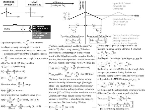
Figure 13.1: Derivation of output voltage ripple of Buck for small capacitances and no ESR/ESL.
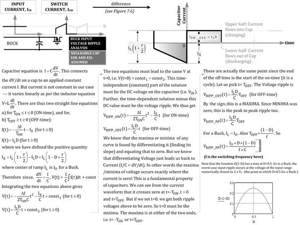
Figure 13.2: Derivation of input voltage ripple of Buck for small capacitances and no ESR/ESL.
Since we expect that the cap voltage ripple is analogous to inductor current ripple, we can confirm that if the capacitance is increased, the voltage ripple decreases — just as when L is increased, r (the current ripple ratio) decreases. Similarly, if frequency is increased, both current and voltage ripple tend to decrease as we had indicated on page 1 of this book. However, we now realize we can do some optimization too. For example, for a given voltage ripple target, we can decrease CO provided we increase the frequency. Getting smaller energy-storage components seems to be a basic advantage of using higher switching frequencies. Though that is not the only reason for higher frequencies, as we will see when we discuss voltage regulator modules (VRMs) in more detail in Part 2 of this chapter. On the output side, as we learned in Chapter 12, lowering the values of L and CO increases the bandwidth of the error–correction loop. That in turn causes the transient response of the converter (its response to sudden changes in line and load) to improve. That is a very important requirement in modern “POL” (point of load) converters or “VRMs” (voltage regulator modules). These are modules, typically high-frequency step-down/Buck converters, mounted on the same board as the converter’s intended load. The load could be a modern microprocessor IC, requiring a very low but tightly regulated voltage rail with very high dI/dt capability.
In Figure 13.3, we plot out both the input/output voltage ripples using Mathcad, with the equations derived in Figures 13.1 and 13.2. In particular, we see how the output voltage ripple is a composite of two curves, one for the ON-time and one for the OFF-time — with both segments meeting “just in time,” at the exact moment where the switch turns OFF and the diode turns ON (which is t=0 as per our convention). The two segments also have the same absolute value at t=–TON (just as the switch turns ON) and at t=TOFF (just as the diode turns OFF). That is why the cycle can repeat endlessly and conform to a “steady state”. In Figure 13.3, we have also plotted out the capacitor currents (input and output) just for comparison, the individual segments and the final curve (shaded). Note that the input current waveform in Figure 13.3 is vertically flipped compared to the corresponding input cap current waveform shown earlier in Figure 7.6. By convention, cap charging current is usually considered positive, and discharging is connected to negative current. But we keep in mind that flipping any given waveform vertically does not change its RMS value, since RMS uses the square of current anyway. So, the sign convention, if any, doesn’t really matter here.
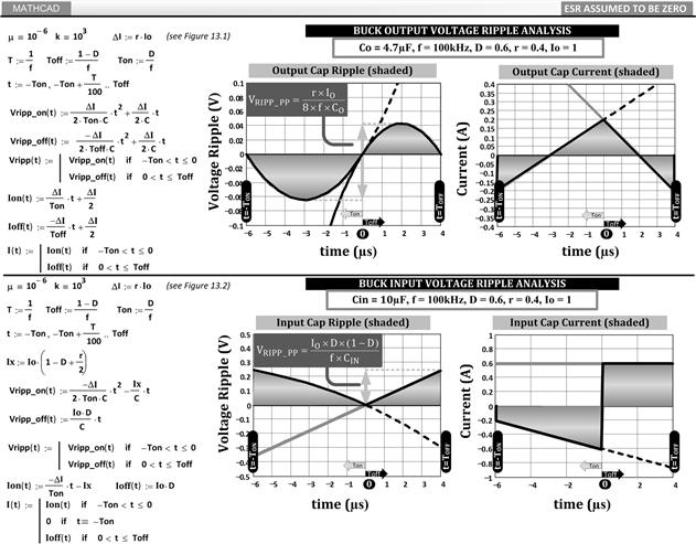
Figure 13.3: Plotting input/output capacitor current and voltage ripple (zero ESR/ESL).
In Figure 13.4, we return to the input ripple, and show how ESR affects it. The total ripple is now a simple sum of two terms, one related to ESR and one to the capacitance charging and discharging. In Figure 13.5, we take the output ripple, and add both the ESR and ESL terms successively to show how the waveform changes at each step. Note that in this latter case (output ripple) the total output voltage ripple is not a simple arithmetic sum of individual terms, because of the phase difference between the components.
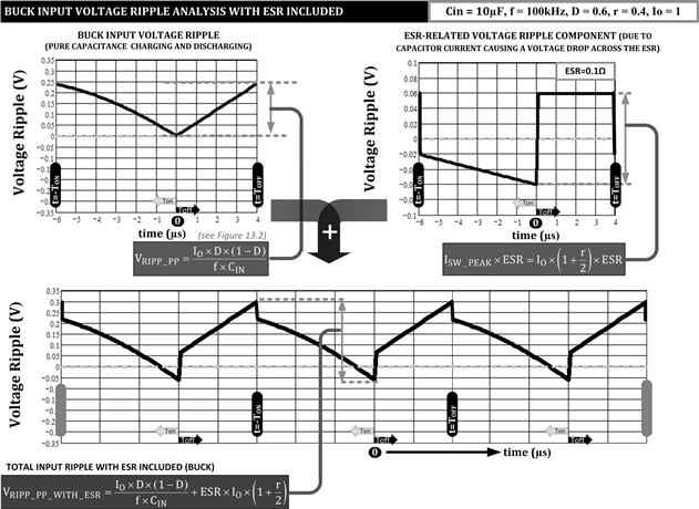
Figure 13.4: Plotting input voltage ripple of Buck with ESR included.
Figure 13.5: Plotting output voltage ripple of Buck with ESR and ESL included.
Both input and output voltage ripples are important. For example, VIN is usually used to provide power to both the converter controller IC, and the power converter stage (switch and inductor). To avoid erratic functioning of the controller IC, we need to not only add a 0.1 μF ceramic cap very close to the supply pin of the IC (decoupling), but also provide an input bulk capacitor sized such that the peak-to-peak input voltage ripple ΔV/VIN is less than 1%. Sometimes, a single, large ceramic capacitor can do “double-duty,” and provide both decoupling and bulk capacitance functions. The acceptable input percentage voltage ripple actually depends on the particular switcher IC/controller: its design, its noise rejection capabilities, the IC package construction, the PCB layout, and so on. We may need to rely on guidance from the IC vendor here. Voltage ripple on the output cap is important too, because it can cause the circuits powered by the output rail to misbehave. For example, a typical power supply specification will call for the ripple on a 5 V output rail to be less than ±50 mV. That is a peak to peak of 100 mV, or a percentage (peak to peak) ripple of 0.1/5=2% — which is sometimes referred to as ±1%, but often colloquially, simply as 1% (just as we do for “1% resistors”).
With all these considerations in play, what is now the dominant criterion for selecting capacitors? In a Buck, the input capacitor’s RMS current is much higher than the output capacitor’s RMS. So, rather generally speaking, we can say that in a Buck, the input cap is determined mainly by RMS stress requirements, whereas on the output, it is simply maximum allowed voltage ripple that determines the capacitance and thereby the capacitor. We can read the sections on capacitor RMS in Chapter 7 to refresh our memory. However, modern ceramic caps have very high RMS ratings, in which case, on the input side of a Buck, the maximum input peak-to-peak voltage (input voltage ripple) becomes the dominant criterion for selecting the capacitor. Lifetime predictions in electrolytic caps are discussed in Chapter 6. In Chapter 9, we discussed hysteretic converters, which are based on a certain output ripple to provide the ramp. In Parts 2 and 3 of this chapter we will learn how to apply these ripple concepts to interleaved converters. The perceptive engineer will be able to go back to Figures 13.1 and 13.2 and derive the necessary ripple equations for the Boost and the Buck-Boost if so desired. Though keep in mind that in many cases, engineers simply assume a large capacitance, and base the estimated voltage ripple on the following simple generic equation
![]()
We can use the peak-to-peak current equations found in the Appendix of this book for each topology.
See “Solved Examples” in Chapter 19, in particular refer to Figure 19.4 for additional criteria for selection of output capacitors in modern Buck converters.
Part 2: Distributing and Reducing Stresses in Power Converters
Overview
Intuitively, we realize that two relatively frail persons can carry a heavy suitcase if they combine forces intelligently, say by holding the suitcase evenly from both sides. So, now we start considering ways to distribute/share stresses by the process of paralleling. First we apply that concept to components. Thereafter, in Part 3, we try to parallel complete sections of converters, called “interleaving” or “multiphase operation”. Finally, in Part 4, we discuss passive and active load sharing in which we parallel entire converters.
Many techniques have evolved over the years to distribute current and voltage stresses across several “identical” components. Discrete components are typically placed in parallel to split/share current stresses, and in series to split voltage stresses. For example, diodes are often paralleled for high current applications. It is best if they are in the same package though. The 2-switch Forward (“asymmetric half-bridge”, see Table 7.1) is an example of two FETs in series, sharing voltage stress equally. The FETs just happen to be on opposite sides of the Primary winding, so the voltage sharing is perhaps not so obvious. But look at it this way: for example, if the input voltage rail is say VIN, and both the switches turn OFF, the voltage across the Primary winding flips from VIN to –VIN. Though it still has seemingly (reverse) VIN across it, what has really happened is that the end of the transformer winding that was initially at ground (when both switches were ON), jumps up to VIN, and the end which was initially at VIN falls to ground. So the total change in voltage is actually VIN – (–VIN)=2×VIN. However, each switch sees a max of only VIN across it. Yet a voltage of 2×VIN is being effectively blocked, by two FETs. Compare that with a single-ended Forward converter with a simple 1:1 energy recovery (tertiary) winding — in that case we have a single switch that blocks the entire 2×VIN. In other words, in a 2-switch Forward, there is subtle voltage stress sharing in effect — but more of a “what could have been” versus a “what is” situation. Similarly, capacitors are sometimes placed in series to share voltage. In a flyback, several caps may be paralleled to handle the rather severe output cap RMS current of this topology. In all cases, a key concern is to get the components to share properly. Sure: “identical” components are really not as identical as we wish. But yes, it really helps if the components were fabricated in the same production lot, preferably in the same package (for FETs or resistors), but even better: fabricated on the same die (or substrate). At every step, they become more and more identical, and their relative matching and stress-sharing capability improves. In more complicated cases, to enforce better sharing, we may need to employ techniques that are either active (as discussed in Part 3), or passive (with the help of ballasting resistors, for example). Take a look at Figure 13.6, which surveys some common component stress-sharing techniques, along with methods to ensure better sharing. Note that very often, there is a smart “correct” way to get them to share well, and a relatively “incorrect” way. Look at the bridge rectifier case for example.
Figure 13.6: Survey of popular techniques to share stresses.
Since in any converter, the actual current stresses are usually proportional to the load current (not so in synchronous converters at light loads though), the question arises: can we just split the load current (of a single power-train) into two identical paralleled converters, to achieve halving of stresses in each? If so, what would be the advantage of that? We take that up shortly (Figure 13.7).
Figure 13.7: Advantages of interleaving (the graph is in terms of unit Ampere load current).
Power Scaling Guidelines in Power Converters
First let us understand how power supplies “scale” with load (in CCM but with no negative current regions as were shown in Figure 9.1). Let us take one of the equations we derived in Chapter 7 to illustrate something quite interesting and useful here. Let us take the RMS of the Buck converter switch current for example. We have shown in Figure 7.3 that

We do remember that, by definition, r=ΔI/IL, where IL is the center of ramp (DC value) of inductor current. In the case of a Buck, IL=IO. So, we can also write the above equations as

The latter equation is seen more commonly in literature. Notice that it looks “messier” than our simpler-looking equations expressed in terms of r. But cosmetics aside, the usual way of writing out the RMS currents also misses out a potentially huge simplification. Because, in contrast, by using r, we can express the switch RMS current in a more intuitive manner — as a product of three relatively orthogonal terms: (a) an AC term, that is, a term involving only r, multiplied by (b) a DC term, that is, one involving only load current IO, and (c) a term related to duty cycle D, as expected. We can thus separate the terms and reveal the underlying concept of power scaling in DC–DC converters, something which is very hard to see from the usual way of writing out the RMS equations as indicated above.
Using our unique method of writing out the RMS current stress equations, we now recognize the fact that current stresses (AVG and RMS) are all proportional to load current (for a given r and fixed D). We thus start to realize what scaling implies. For example, this can mean several things:
• In terms of ability to handle stresses, a 100 W power supply will require an output capacitor roughly twice, in terms of capacitance and size, compared to a 50 W power supply (for the same input and output voltages). Here we are assuming that if we are using only one output capacitor, its ripple current rating is almost proportional to its capacitance. That is not strictly true though. More correctly, we can say that if a 50 W power supply has a single output capacitor of value C with a certain ripple rating IRIPP, then a 100 W power supply will require two such identical capacitors — each of value C and ripple rating IRIPP, paralleled together. That doubles the capacitance and the ripple rating (ensuring the PCB layout is conducive to good sharing too). We could then justifiably assert that output capacitance (and its size) is roughly proportional to IO. Note that we are implicitly assuming switching frequency is the same for the 50 W and 100 W converters. Changing the frequency can impact capacitor selection, as we will see shortly.
• Similarly, rather generally speaking, a 100 W power supply will require an input capacitor twice that of a 50 W power supply. So, input capacitance (and its size) will also be roughly proportional to IO. But more on this shortly too.
• Since heating in a FET is ![]() , and IRMS is proportional to IO, then for the same dissipation, we may initially think we would want a 100 W power supply to use a FET with one-fourth the RDS of a 50 W supply. However, we are actually not interested in the absolute dissipation (unless thermally limited), only its percentage. In other words, if we double the output wattage of a converter, say from 50 W to 100 W, we typically expect/allow twice the dissipation too (i.e., the same efficiency). Therefore, it is good enough if the RDS of the FET of the 100 W power supply is only half (not quarter) the RDS of the FET used in the 50 W power supply. So in effect, FET RDS is inversely proportional to IO.
, and IRMS is proportional to IO, then for the same dissipation, we may initially think we would want a 100 W power supply to use a FET with one-fourth the RDS of a 50 W supply. However, we are actually not interested in the absolute dissipation (unless thermally limited), only its percentage. In other words, if we double the output wattage of a converter, say from 50 W to 100 W, we typically expect/allow twice the dissipation too (i.e., the same efficiency). Therefore, it is good enough if the RDS of the FET of the 100 W power supply is only half (not quarter) the RDS of the FET used in the 50 W power supply. So in effect, FET RDS is inversely proportional to IO.
• We also know that for any power supply, we usually always like to set r≈0.4 for any output power. So, from the equations for L, we see that for a given r, L is inversely proportional to IO. Which means the inductance of a 100 W power supply choke will be half that of a 50 W power supply choke. L is therefore inversely proportional to IO. Note that here too, we are implicitly assuming switching frequency is unchanged. Also that the output LC product does not depend on load.
• Energy of an inductor is (1/2)×L×I2. If L halves (for twice the wattage) and I doubles, then the required energy-handling capability of a 100 W choke must be twice that of a 50 W choke. In effect, the size of an inductor is proportional to IO. Note that since L is dependent on frequency, we are again implicitly assuming that the switching frequency is unchanged here.
Concept behind Paralleling and Interleaving of Buck Converters
Hypothetically, at an abstract level, suppose we somehow implement sharing exactly (however we do it): for example suppose we have somehow managed to implement two paralleled, identical converters, each delivering a load current IO/2. This is Case C in Figure 13.7. Both power-trains (individual converters) are connected to the same input VIN and the same output VO. They are driven at the same frequency (though the effect of synchronization, if any, between these two “phases”, is only on the input/output caps as discussed later). First we show that in terms of inductor volume, paralleling may even make matters worse.
We know (or assume for now) from optimization principles, that for each inductor, r should be set to about 0.4. Since the two paralleled converters carry only IO/2, we need to double the inductance of each, to achieve the same current ripple ratio for each inductor, and that is commensurate with the inductance scaling rule explained above.
Now, let us look at the energy-handling capability of each of the two inductors above. That is proportional to LI2, and that gets halved — because I halves and L doubles. We also have two such inductors. So the total core volume (both inductors combined), is still unchanged from the volume of the single inductor of the original single power-train (the latter is Case A in Figure 13.7).
Note that in literature, it is often stated rather simplistically, that “interleaving helps reduce the total volume of the inductors.” The logic they offer is as follows:
Single converter inductor with current “I”:
![]()
Two phases, each inductor carrying half the current:
![]()
So, it is said the total inductor volume halves due to interleaving. Yes, it does, but only for two inductors each with an inductance equal to that of the single converter. However now, each phase is carrying half the current, and if we do not change L, the ΔIL remains the same, but IL (center of ramp) is half, so the current ripple ratio ΔIL/IL is doubled! If we are willing to accept the higher current ripple ratio in a single-inductor converter, we would get the same “reduction in volume.” That has actually nothing to do with the concept of interleaving. It is a basic misunderstanding of energy storage concepts as detailed in Chapter 5. Therefore, the above “logic” is a fallacy.
What exactly do we gain in using Case C (paralleled converters) instead of Case A (single converter)? In terms of the inductor volume required to store a certain amount of energy, there seems to be no way to “cheat” physics. We learned in Chapter 5 that for a given output power requirement and a given time interval T (=1/f), the energy transferred in a certain time interval t is ε=PO×t. Yes, we can split this energy packet into two (or more) energy packets each handled by a separate inductor. But the total energy transferred in interval “t” must eventually remain unchanged, because ε/t (energy/time) has to equal PO, and we have kept output power fixed in our current analysis. Therefore, the total inductor volume (of two inductors) in Case C is still ε (because 2×ε/2=ε). Note that just for simplicity, we assumed the logic of a flyback above, since as we had learned in Chapter 5, its inductor has to store all the energy that flows out of it (or we need to include D in the above estimates too; but the conclusions remain unchanged for any topology).
Yes, we could double the frequency and spread the energy packets more finely. We thus get Case B, and remain a single converter. Only this time, instead of two ε/2 packets every interval T, we need to store and transfer one packet of size ε/2 every T/2. In effect, rather intuitively speaking, we are using the same inductor to first deliver ε/2 in T/2; then re-using it to deliver the next ε/2 in T/2. “Time division multiplexing” in computer jargon. So eventually, we still get a total of ε Joules in T seconds as required (equivalently, PO Joules in 1 s, to make up the required output power). However, (only) one inductor is present to handle ε/2 at any given moment. So, total inductor volume halves in Case B, as indicated in Figure 13.7.
However, going back and comparing situations belonging to the same switching frequency (i.e., Case A and Case C), we now point out that in practice, as opposed to theory, paralleling two converters may end up requiring higher total energy storage capability (and higher total inductor volume) — simply because there is no such thing as perfect sharing however “smart” our implementation may be. For example, to deliver 50 W output, two paralleled 25 W rated converters just won’t do the job. We will have to plan for a situation where due to inherent differences, and despite our best efforts, one power-train (called a “phase”) may end up delivering more output watts, say 30 W, and the other correspondingly, only 50–30=20 W. But we also don’t know in advance which of the two power-trains will end up carrying more current. So we will need to plan ahead for two 30 W rated converters, just to guarantee a 50 W combined output. In effect, we need a total inductor volume sufficient to store 60 W, as compared to a single converter inductor that needs to store only 50 W. Hence, we actually get an increase in inductor size due to paralleling (for the same current ripple ratio r).
So why don’t we just stick to doubling the frequency of a single converter? Why even bother to consider paralleling converters? Nothing seems to really impress about paralleling so far. Well, we certainly want to distribute current stresses and the resulting dissipation across the PCB to avoid “hot-spots”, especially in high-current point-of-load (POL) applications. But there is another good reason too. Looking closely at Case C in Figure 13.7 we note that the output current waveform is sketched with an AC swing that is described as “very small.” No equation or number was provided here, and for good reason. We remember the output current is the sum of the two inductor currents. Suppose we visualize a situation where one waveform is falling at the rate of X A/μs, and the other simultaneously rising at the rate of X A/μs. If that happens, clearly the sum of the two will remain unchanged — we will get pure DC with no AC swing at all. How exactly can that happen? Consider the fact that in steady state, for a Buck, the only way the falling slope (–VO/L) of the inductor current can be numerically equal to the rising slope ((VIN–VO)/L), is if VIN–VO=VO, or VIN=2×VO, that is, D=50%. In other words, we expect that at D=50% the output current ripple will be zero! Since for fairly large C, the voltage ripple is simply the inductor current ripple multiplied by the ESR of the output cap, we expect low output voltage ripple too. That is great news. See Figure 13.7 for the graphed output current ripple (peak to peak) on the lower right side (Mathcad generated plot). It has a minimum of zero at D=50% as intuitively explained above.
We see that the output current ripple, and therefore the output voltage ripple, can be significantly reduced by “interleaving” — this means running the two converters with a phase shift of 180° (360° is one full clock cycle). But it also turns out that the input RMS current is also almost zero at D=50% (see graph in Figure 13.7). The reason for this is that as soon as one converter stops drawing current, the other starts drawing current, so the net input current appears closer and closer to DC as duty cycle approaches 50% (except for the small AC component related to r). In other words, instead of the sharp edges of switch current waveforms that usually affect the input cap current waveforms of a Buck, we now start approaching something more similar to the smoother undulating waveforms typically found on the output cap. All these improvements are graphed in Figure 13.7 while comparing Case A to Case C (i.e., single converter of frequency f versus two paralleled ones, each with frequency f but phase shifted as indicated by the Gate drive waveforms). The graph in Figure 13.7 is the result of a detailed Mathcad worksheet, described in Figures 13.8 and 13.9. The waveforms from this worksheet are further shown for two cases in Figure 13.10 for a numerical example.

Figure 13.8: Mathcad file (Part 1) for interleaved Buck converters as graphed in Figures 13.7 and 13.10.
Figure 13.9: Mathcad file (Part 2) for interleaved Buck converters as graphed in Figures 13.7 and 13.10.
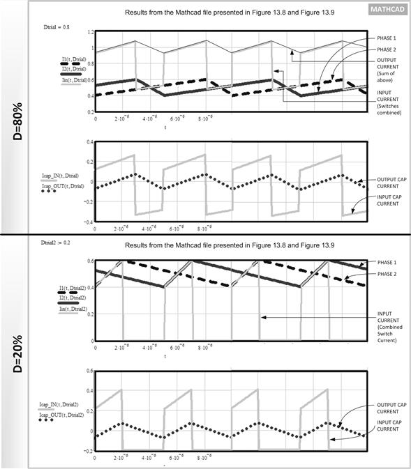
Figure 13.10: Key waveforms of interleaved Buck converters.
Note that we have made an assumption above, that the two converters switch exactly out of phase (180° apart, i.e., T/2 apart). As mentioned, this is called “interleaving,” and in that case each power-train is more commonly referred to in literature as one “phase” of the (combined or composite) converter. So in Case C of Figure 13.7, the “converter” has two phases. We could also have more phases, and that would be generically, a multiphase (N-phase) converter. We have to divide T by the number of phases we desire (T/N), and start each successive converter’s ON-time exactly after that sub-interval. If we run all the power-trains (i.e., phases) in-phase (all ON-times commencing at the same moment), the only resulting advantage in this case is we distribute the heat around. But interleaving reduces overall stresses and improves performance. From the output capacitor’s viewpoint, the frequency effectively doubles, so the output ripple is not only much smaller, but can even be zero under the right duty cycle conditions.
At the input side, it is not the peak-to-peak ripple, but the RMS current that is very important. In general, RMS of a waveform is independent of frequency. However, interleaving does reduce the input RMS stress. That happens not due to any frequency doubling effect but because interleaving ends up changing the very shape of the input current waveform — to something closer to that of a steady stream of current (a gradual removal of the AC component depending on duty cycle).
One drawback of interleaving as described so far, is that the inductors each still “see” a switching frequency of 1/f, as is obvious from their current ripple (their up-slope and down-slop durations). But later, using coupled inductors, we will discuss how we can “fool” the inductors too, into “thinking” they are at a higher switching frequency.
Closed-Form Equations for RMS Stresses of Interleaved Buck Converter
Now for some simple math to validate the key curves in Figure 13.7, and also to derive closed-form equations. The equations that follow can be “rigorously derived” over several rather intimidating pages if so desired. Such derivations are readily available in related literature. Here we do the same, but intuitively, and hopefully more elegantly, if not very rigorously.
(a) First let us look at the output capacitor ripple. We know that in single-phase converters, since TOFF=(1−D)/f, the current ripple is ΔI=(VO/L)×[(1−D)/f]. So the peak-to-peak ripple depends on 1–D. Now if we look closely at Figure 13.7, we will realize that looking at the combined output current, it certainly has a repetition rate of 2f just as we expected, but its duty cycle is not D, but 2D. That is because the ON-time of each converter has remained the same, but the effective time period has been cut in half. So, the effective duty cycle for the combined output current is TON/(0.5×T)=2×TON/T=2D. Since peak to peak ripple (ΔI) is proportional to 1−D, for the combined output it becomes
![]()
![]()
This is true when the switch waveforms of both phases do not overlap, that is, D<50%. Which means the ON-durations of the two phases are separated in time. Of course, in that case, the OFF-durations are the ones that overlap. Recognizing this symmetry, we can actually quickly figure out what happens when the reverse happens, that is, when the switch waveforms overlap, or when D>50%. Because then the OFF-times do not overlap. We keep in mind that these are just geometrical waveforms. There is no significance to what we call the ON-time and what we call the OFF-time as far as the waveforms go. Therefore, we can easily reverse the roles of D and D′, just as we did long ago in Figure 7.3. So, now we can easily guess what the peak-to-peak ripple relationship is for the case D>50%, that is, for the case D′<50%! We thus get
![]()
Note that this represents a current ripple reduction for the combined output of the interleaved Buck, compared to the current ripple of each of its two phases (we are not comparing this with the single converter case anymore).
(b) Now let us look at the input cap RMS current. From the viewpoint of the input capacitor, the switching frequency is again 2f, and the duty cycle is 2D. The current is drawn in spikes of height IO, which is 0.5 A for every 1 A (combined) output current. We are using the flat-top approximation here (ignoring the small term involving r). From Figure 7.6, for a Buck, we can approximate the input cap RMS as
![]()
So for the interleaved converter, though changing effective frequency has no effect on the RMS stress of the input cap, the effective doubling of duty cycle profoundly affects the wave shape and the computed RMS. We get the following closed-form equation:
![]()
where IO is the output current of each phase (half the combined current output). When the waveforms overlap, using the same logic as above, we can easily guess the input cap RMS as
![]()
To cement all this, a quick numerical example is called for.
Example:
We have an interleaved Buck converter with D=60%, rated for 5 V at 4 A. Compare the output ripple and input cap RMS to a single-phase converter delivering 5 V at 4 A.
Single-Phase Case: We typically set r=0.4. So for 4 A load, the inductance is chosen for a swing of 0.4 A×4 A=1.6 A. That is just the peak-to-peak output current ripple. This agrees with Figure 13.7, which is for 1 A load. So, scaling that four times for a 4 A load, we get 0.4 A×4 A=1.6 A.
The input cap RMS with flat-top approximation is from our equation
![]()
This also agrees with the Mathcad-based plot in Figure 13.7 in which we get about 0.5 A at D=0.6 for 1 A load. Scaling that for 4 A load current, we get 0.5 A×4 A=2 A RMS; slightly higher than the 1.96 A result from our closed-form equation.
Interleaved Case: This time we split the 4 A load into 2 A per phase. The reduction in ripple equation for D>50% gives us a “ripple advantage” of
![]()
The peak-to-peak ripple of each phase is 0.4 A×2 A=0.8 A. Therefore, the ripple of the combined output current must be 0.333 A×0.8 A=0.27 A. Comparing with the plot in Figure 13.7, we have at D=0.6, a peak-to-peak ripple of 0.067 A. But that is for 1 A load. So, for 4 A load we get 4 A×0.067 A=0.268 A, which agrees closely with the 0.27 A result from the closed-form equation. Now calculating the input cap RMS from our equations, we get
![]()
Comparing with the plot in Figure 13.7, we get at D=0.6, input cap RMS to be 0.2 A. But that is for 1 A load. So, for 4 A load we get 4 A×0.2 A=0.8 A, which agrees exactly with the 0.8 A result from the closed-form equation.
We have shown that the results of the Mathcad spreadsheet agree with the closed form equations above (intuitively derived). We can use either of them.
Summarizing, we see that for a single-phase converter the output current ripple (peak-to-peak) was 1.6 A, and the input cap RMS was 2 A. For the interleaved solution, output ripple fell to 0.27 A, and the input cap RMS fell to 0.8 A. This represents a significant improvement and shows the beneficial effects of interleaving (paralleling out-of-phase).
We remember that in a Buck, the dominant concern at the input cap is mainly the RMS stress it sees, whereas on the output, it is the voltage ripple that determines the capacitance. So, interleaving can greatly help in decreasing the sizes of both input and output caps. The latter reduction will help improve loop response in the bargain — smaller L and C components charge and discharge faster, and can therefore respond to sudden changes in load much faster too. But besides that, we can also now revisit our entire rationale for trying to keep inductors at an “optimum” of r=0.4. We recall that was considered an optimum for the entire (single-phase) converter (see Figure 5.7). But now we can argue that we don’t have a single converter anymore. And further, if we are able to reduce RMS stresses and the output ripple by interleaving, why not consciously increase r (judiciously though)? That could dramatically reduce the size of the inductor. In other words, for a given output voltage ripple (not inductor current ripple), we really can go ahead and increase r (reduce inductance) of each phase. We already know from Chapter 5 that reducing inductance typically reduces the size of the inductor for a given application. Certainly, the amount of energy we need to cycle through the total inductor volume is fixed by physics as explained in Chapter 5. However, the peak energy storage requirement significantly goes down if we decrease inductance (increase r). That was also explained as part of the magnetics paradox discussed in Chapter 5.
One limitation of increasing r is that as we reduce load, we will approach discontinuous conduction mode (DCM) for higher and higher minimum load currents. That is why we have used synchronous Buck converters in Figure 13.7 to illustrate the principle of interleaving. As we learned in Chapter 9, most synchronous converters never go into DCM; they remain in CCM right down to zero load current condition (even getting down to sinking the load current if necessary). The efficiency suffers of course, but it works at constant frequency and the effects of interleaving will still apply. Another advantage of intelligent multiphase operation is that at light loads we can start to “shed” phases — for example, we can change over from say a six-phase multiphase converter to a four-phase converter at medium loads, and then go to a two-phase converter at lighter loads, and so on. That way we reduce switching losses, because, in effect, we are reducing overall switching frequency, and thereby greatly improving light-load efficiency.
Interleaved Boost PFC Converters
In Chapter 9, in particular in Figures 9.1–9.3, we had shown that a Boost is just a Buck with input and output swapped. Therefore, now that we have derived all the equations for synchronous interleaved Buck converters, there is no reason why the very same logic and equations can’t be used for a synchronous interleaved Boost stage. The mapping we need to do is D↔(1−D), VIN↔VO, and IO↔IO/(1−D), since the ON-time of a Buck becomes the OFF-time for the corresponding Boost. We just apply this mapping to the stress equations derived above.
In Chapter 14 we will discuss power factor correction (PFC) using a Boost converter. Now we can see that for higher power stages, not only can we parallel FETs as described in Figure 13.6, but we can get significant reduction in input and output capacitor size by interleaving (using two phases), just as we have done for the Buck converter above.
In a PFC stage the analysis is harder to do because of the sine wave input. Actual lab measurements provide the following useful rule-of-thumb: the output cap RMS current is halved due to interleaving, as compared to a single-stage Boost PFC stage.
Interleaved Multioutput Converters
The concept of interleaving has been arbitrarily “extended” to include cases where each power-train delivers a different output voltage. Check out the LM2647 for example. Clearly, now the output capacitor/s cannot be shared. But the vendors of such ICs claim dramatic improvements in the RMS of the shared input cap as a justification for this multioutput interleaved architecture. But how exactly do they “prove” lower input RMS current on paper? They do it by loading both power-trains to maximum rated load, and computing the RMS of the resulting input cap waveform. Yes, they do get a lower overall input capacitor size compared to completely separated power-trains. However, on closer examination that “RMS reduction” can be misleading — because as we pointed out, we have to be wary of stresses that do not have a maximum at extreme corners of line and load. In fact, capacitor RMS fits right into that category. In this case, if we unload one output, and only load the other (to its max load), we usually get much higher input cap RMS current than if both outputs were fully loaded. So what exactly did we gain? Nothing! And besides that logical problem, when we share one input cap between multiple outputs, we cannot but avoid cross-coupling of the two output channels. For example, if one output suddenly sees a load transient, its input cap voltage wiggles a bit, and since that is intended to be the input cap for the other power-trains too, some of that wiggle gets transmitted to the other output rail too. This is called cross-coupling, and the only solution is to actually provide completely separate input capacitors, placed very close to the input of each power train, and to separate those capacitors for high frequencies, either through long PCB traces, or actual input inductors, star-pointing at the input voltage source, which usually has another bulk capacitor at the point where it enters the PCB. In other words, the “advantage,” if any, of this multioutput interleaved converter, can be almost non-existent at a practical level. Really, the product definition is itself flawed in this case. The datasheet of LM2647 was written by this author actually, and the above product definition problem was pointed out and explained in the datasheet.
Part 3: Coupled Inductors in Interleaved Buck Converters
Overview
So far we have only considered the configuration in which the two power-trains (or phases) are joined together “at their ends,” thus impacting the input and output capacitors (beneficially it turned out). That is Case C in Figure 13.7. In between, where the inductors lie, the power-trains are still completely independent. That is why the inductors still had a current ripple based on f, not on 2f for example. We can now visualize that the effects of interleaving (coupling) can be felt on the inductors if we somehow bring them together instead of having them fully independent. The only way to do that practically is through a non-physical connection, that is, through magnetic coupling.
This area is of great interest in modern voltage regulator modules (VRMs). Multiphase converters, often with proprietary magnetic structures, are getting increasingly popular as a means of providing the huge dI/dt’s demanded at sub-volt levels by modern microprocessor (“μP”) ICs. The constraints for VRMs are slightly different. Efficiency is always important of course, since a lot of processing equipment is battery-powered. But besides that, of great importance is the very tight regulation and extremely fast transient response (minimal overshoot or undershoot in response to sudden changes in load). Another driving concern is to make the VRM compact. So, putting several windings on a shared core seems to be of natural interest. Note that in fact, the output voltage ripple of the VRM (i.e., the input ripple to the μP), is not of such great concern here, since we are usually not powering any extremely noise-sensitive analog chips. And in any case, if we do need such a quiet rail locally for certain functions, that can always be derived by using a small post-filter (LC- or RC-based) off the main rail.
There are many ways to couple the windings of the inductors. However, to avoid a rather unnecessary and intimidating discussion, we will focus on trying to understand the currently popular technique called “inverse coupling.” Also, we will focus only on two-phase converters here. But once the concepts are understood those ideas can easily be extended to N-phases. We will also initially restrict ourselves to more common application with non-overlapping switch waveforms (D<50% for a two-phase converter). But finally, we will cover the area of overlapping switch waveforms too (i.e., D>50%).
Before diving into some fairly complex but unavoidable math, a practical implementation of inverse coupling is illustrated in Figure 13.11. Both direct and inverse coupling are explained in Figure 13.12. Here are the points to note as we go along in our development of our concepts and ideas.
• Note the direction of the windings in Figure 13.11. Part of the flux from one winding goes through the other winding and opposes the flux from the other winding. The opposing flux contributions (in the outer limbs), however, do not rise and fall in unison, because they are out-of-phase (interleaved). But their relative directions do indicate inverse (opposing) coupling.
• There is typically a certain air gap provided on (both) the outer limbs, but also another air gap of a different gap-length provided on the center limb. By increasing the air gap on the center limb for example, we can make more flux go through the outer limbs, and that will increase the amount of (inverse) coupling. This is one way to adjust (fine-tune) the “coupling coefficient” k. Think of flux mentally as water flowing in pipes. If we block one pipe, it tries to force its way through another. The air gap amounts to a constriction in the pipe.
Note: In a subsequent figure (the Mathcad file in Figure 13.15), we have called the coupling coefficient “α” instead, to avoid confusion with the “k” used for kilo in that file.
• Figure 13.12 represents one easy model used to represent coupled inductors. “M” is the mutual inductance. Keep in mind it is just one of many models out there used to help better understand coupled inductors. Other models can get even more intimidating, and besides, none of the models are considered perfect — they all have pros and cons. Some are “non-symmetrical models” and even harder to digest. For example, the question lingers why two supposedly identical windings look so different from each other. In our model too, the node between L and M is a “fictitious node.” In a way, we have resorted to fiction to understand reality! That is why we don’t really proceed much further down this path of models, except to find the starting-point equations for later analysis.
• In Figure 13.13, we write out the same equations for inverse coupling shown in Figure 13.12, but then actually analyze the actual relationships between V1 and V2 (the voltages across the inductors of the respective phases), as we switch the FETs. We examine the voltages across the inductors, and thus identify four possible states (called A, B, C, and D). Of these, one (D) is actually identical to B (look at their voltages V1 and V2). In other words, whatever we work out for B will apply to D. So, there are just three distinct states that we need to study further, not four. These are A, B, and C.
• We know the effect of the mutual inductance on the three states (A, B, and C), from the equations we wrote for inverse coupling. And we also know the actual voltages that appear across the (actual) inductors in the three states. Note that at this point we are trying to connect our real-world (actual) inductor with the inverse coupling model. And we thus find that over each of these three states, the simple equation V=L dI/dt no longer seems to apply. In other words, the slopes (dictated by the inverse coupling equations) do not match the assumed inductance L any more (because we realize that one winding influences the other, and vice versa).
• We follow this through and try to reconcile matters. So, now we say that if we are to somehow force V=L dI/dt to be still true (artificially), we need to re-define or re-state inductance (since dI/dt is known, and so is the applied voltage across the inductor). We thus generate an “equivalent inductance” for each of the three (four) states based on L=V/(dI/dt). We call these LA, LB, LC (and LD which we know just equals LB). The equations for equivalent inductance in all three states are provided in Figure 13.13. Note from the derivations of equivalent inductances, these inductances apply even if D>50%, as discussed later (Figure 13.16).
• In Figure 13.14, we take this concept of equivalent inductances and calculate the change in output (combined) ripple due to coupling (“CPL,” compared to the uncoupled case denoted as “UCPL”). We get
![]()
(This is for the combined output — into the output cap). We see that since k varies from 0 (no coupling) to 1 (max coupling), the output ripple change will always be greater than 1. So, (inverse) coupling will always cause the ripple of the combined currents (i.e., the output ripple) to worsen as compared to the uncoupled (interleaved) case. That seems understandable, if not desirable, since in a way, by inverse coupling, we cancel some of the inductance out, so we do expect higher ripple. As mentioned, that is typically acceptable in modern microprocessors so long as we stay within a tight regulation window (by good transient response and/or droop regulation methods as discussed in Part 4 of this chapter).
• Looking in from the output side into the converter, we can confirm through simulations, that it does seem that a smaller inductance is now driving the output current. Simulations also confirm that this lowered inductance is also accompanied by a great improvement in transient response. All that is intuitively expected, since we know smaller L and C’s can charge and discharge more rapidly, and therefore don’t “come in the way” of quickly dumping more energy into the load (a positive dI/dt), or removing energy (negative dI/dt). We can do some more detailed geometrical calculations (not shown here) to see how the current at the end of a switching cycle ramps up (“ΔIX”) as compared to the current at the start of the cycle, due to a small and sudden increase in duty cycle (ΔD), on account of a sudden load demand. The results of that are quoted here:
![]()
It is indeed surprising that the terms involving LA and LC have canceled out here, leaving only LB. Researchers report they have validated this improvement of transient response through simulations. They have also tried to intuitively explain it, but it is not easy to explain or understand. Note that if the inductors were not coupled, we would have got (since LB is equal to L if k=0)
![]()
Therefore, the improvement in transient response is
![]()
This is exactly the factor by which the (combined) output ripple increased. So that makes sense. Further, since k is between 0 and 1, the coupled transient response must be better than the uncoupled case. For example, if we set k=0.2, we get a 25% improvement in response. For this reason, LB is referred to in literature as the “transient equivalent inductance.” We can think of it intuitively as the “output equivalent inductance.” When there is a sudden change in load, it seems to be coming through a smaller inductance called LB.
• We see that the transient response is good, but the (combined) output ripple has worsened on account of coupling (1/(1–k) above). Note that this statement is true only when compared to an identical interleaved Buck, with the same inductances, but completely uncoupled (i.e., setting k=0). But, wouldn’t we have achieved exactly the same result by simply lowering the inductance L of each phase closer to LB and sticking to simple uncoupled inductors? That is true. But a strange thing happens here that justifies all the trouble. We recall that generally, the RMS on the input capacitor and the RMS of the switch current typically increase as we lower the inductance (because we get more “peaky” waveforms). In the case of coupled inductors, the phase ripple actually decreases on account of coupling”. From Figure 13.14
![]()
So, provided LA is greater than L, the current ripple in each phase decreases. Surprisingly, the phase ripple does not depend on the lower equivalent output inductance LB (mentioned above), but on LA (equivalent inductance during the ON-time). This makes the phase current less peaky and leads to a reduction in the switch RMS current and the RMS of the input cap current. Now, a reduction in switch/input RMS is not intuitively commensurate with a smaller inductance — but a larger inductance. As expressed by the phase ripple expression, we can improve efficiency, despite appearing to reduce output inductance for achieving good transient response. For this reason, LA is sometimes referred to in literature as the “steady-state equivalent inductance.” We can think of it intuitively as the “input equivalent inductance.”
By how much is LA greater than L? From Figure 13.14, the relationship is
![]()
This means we can use our usual equation for the RMS switch current in a Buck FET (see Figure 7.3)
All we need to do here to calculate the RMS switch current for the interleaved coupled inductor Buck is to set IL→IO/2, and L→LA.
• In Figure 13.15, we have plotted out the equivalent inductances. We see that LB is always less than 1 (i.e., L here), indicating better transient response due to coupling. But LA is greater than 1 (i.e., L) only above a certain threshold we have called DZERO here. More on that below.
• In Figure 13.15, we see that LB is always less than L, as expected. Coming to LC, that is actually negative below a certain duty cycle. That too occurs below the threshold DZERO. Note that the inductance LC determines the slope of the wiggle in the phase ripple waveforms (Region C in Figure 13.13). The direction of the wiggle depends on the sign of LC. Exactly at DZERO, LC swings from positive infinite inductance to negative infinite inductance. Which means the current in Region C changes from a slope described as “minus zero” (slightly downwards) to “plus zero” (slightly upwards). At exactly DZERO, the current is flat (i.e., zero slope). Note that in Figure 13.13, we have assumed the phase current waveform in Region C continues to fall. If LC is negative, that would not be serious in itself. However, from Figure 13.14 we see that below a certain “DZERO,” LA is less than L. LA being the “steady-state equivalent inductance” as explained above, this means that now the phase ripple with coupled inductors is worse than the uncoupled case. We have thus lost one major advantage of coupling (other than the fast transient response which could have been achieved simply by using smaller uncoupled inductances). To achieve any improvement in efficiency (and reduction in RMS current in the switch and input cap), we must therefore always operate only in the region D>DZERO. This means that LC must be positive, and so the phase current waveform would look like what we have sketched out in Figures 13.13 and 13.14. The wiggle in Region C should not be upward (positive slope). In the former figure, we have derived the equation for DZERO.
![]()
We can solve this for a max coupling coefficient
![]()
In Figure 13.15 we have also provided the best value for k as a function of D.
• Actually, there is another practical boundary that can occur if the denominator of LA equals zero. We need to avoid that singularity too. Combined with the restriction from avoiding the zero denominator of LC, we can finally define a usable operating area when using inverse coupled inductors. The final result is that the duty cycle of the VRM in steady state should never be set outside the following limits
![]()
Note that just as we call 1–D as D′ sometimes, we can call 1–DZERO as ![]() if we want.
if we want.
• In Figure 13.15, we also have a numerical example. A 200 kHz VRM is stepping down 5 V to 1.2 V using coupled inductors (k=0.2), each of 15 μH. So, the duty cycle is 1.2/5=0.24. We can calculate from the above equation that kMAX=0.32. We ask: what will happen if we have coupling in excess of this value? Looking at the waveforms on a scope, we will then see that the current segment of the Phase 1 inductor current in Region “C” will rise up rather than down. This can be explained through excessive coupling caused by the switch of Phase 2 turning ON. Because when the switch of Phase 2 turns ON, it produces a positive rate of change of flux in its winding, but a negative change (decrease) in flux in the winding of Phase 1. Since change of flux is always to be opposed, Phase 1 suddenly decreases its rate of fall of current, or in the worst-case, even increases its current, just to try to keep the flux through it constant. But with such high coupling, LA, the equivalent input (or steady) inductance becomes less than the uncoupled case inductance, L. So now we have a lower efficiency than the uncoupled case as explained above. That is obviously not a good way to operate.
• In Figure 13.16, we extend our treatment into the region D>50% using the same numerical example as in Figure 13.15 to illustrate what happens over the entire input range. The key observations are as follows:
(a) In Figure 13.13, the derivations for equivalent inductances would apply to the region D>50%, and so those equations are still valid.
(b) The durations of each region are simply flipped according to D↔D′, since any ON-state switch waveform for D<50%, when flipped over vertically become a switch waveform for D>50%. We must note that though the current waveform for D>50% looks very similar (vertically flipped) compared to the D<50% waveform, the two do not have the same magnitudes. Because, with inductors we have to remember that if D increases, that always means input voltage is falling, so the applied voltseconds also decreases, which causes a smaller slope. So naturally, we expect the ripple (AC swing) to decrease progressively as we increase D from close to 0 toward 1. We also see that the phase ripple is not only less than the uncoupled case (looking in the region between DZERO and ![]() ), but the situation gets progressively better (as D increases).
), but the situation gets progressively better (as D increases).
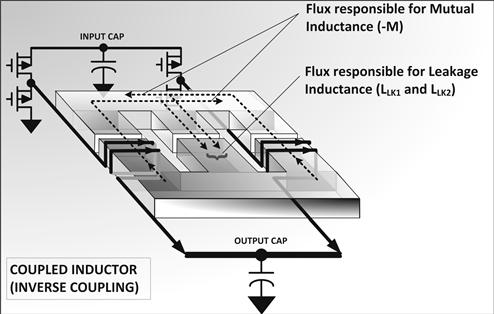
Figure 13.11: Coupled inductor magnetics.
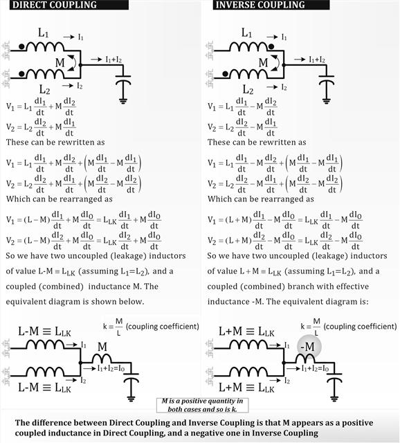
Figure 13.12: Models to explain direct and inverse coupling.
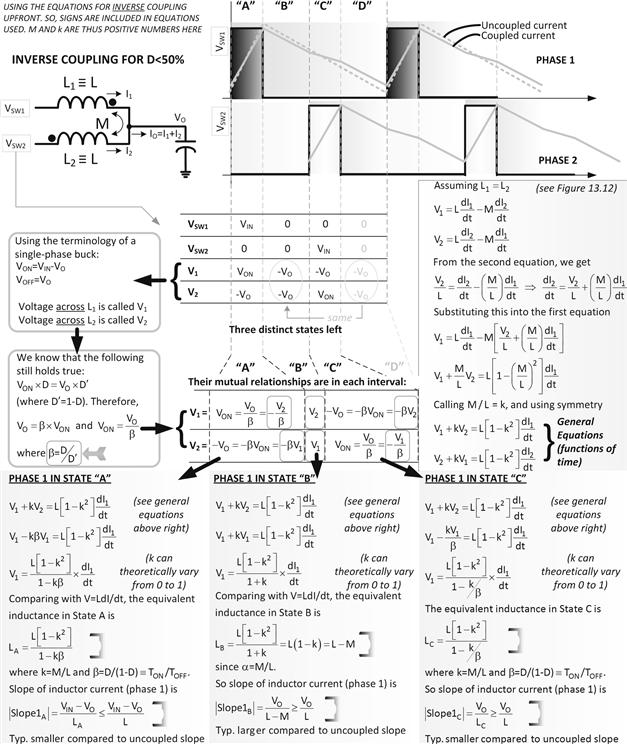
Figure 13.13: Derivations of equivalent inductances and slopes based on coupling coefficient k.
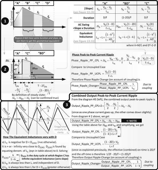
Figure 13.14: Equations for ripple in an interleaved Buck converter with coupled inductors.
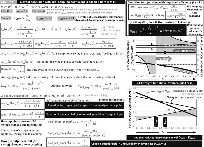
Figure 13.15: Using Mathcad to plot equivalent inductance variations and ripple for coupled inductor Buck converters operating with D<50%.
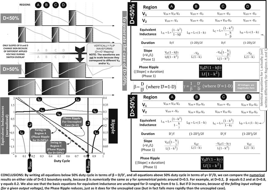
Figure 13.16: Extending our analysis of coupled inductor Buck converters to D>50% (overlapping switch waveforms).
Part 4: Load Sharing in Paralleled Converters
Passive Sharing
Semiconductor vendors often release evaluation boards, such as a stand-alone “5 V at 5 A synchronous Buck converter,” and so on. Many inexperienced engineers are often tempted to try to get 5 V at 10 A by just brute-force paralleling of two such “identical” boards. That never works; they find they may not even be getting 5 V at 5 A anymore, despite complaining rather indignantly to customer support.
The root cause for the strange behavior they may report is the “slight” differences between the two converters. Keep in mind that the error amplifier which is present in every feedback loop, trying to regulate each output to its set value (reference value), is always designed with very high-gain so that it can regulate the output tightly down to a few millivolts of the set value. This error amplifier therefore dramatically amplifies any existing error between the set output and the instantaneous output — much like a watch repairman who examines a “tiny problem” under a very high-magnification microscope, and thereby fixes it. Now consider this: the set output voltages of the two converters are naturally a little different because of tolerances in their resistive dividers (if present), their internal references, and so on. These set values also drift with temperature. So, when the two outputs are connected together, what may be a “natural/appropriate/correct” output voltage for one feedback loop, will likely generate a huge internal error in the feedback loop of the other converter. The two loops will end up “fighting” to determine the final output voltage. If the output “suits” one, the other will complain — by issuing forth a huge swing in its duty cycle, and if it suits the other, the former will complain. Depending on the actual current-sense architecture in use, things may stabilize; but usually they won’t. At best, a strange and uneasy “stable condition” can occur just after power-up. One converter (with the highest set output) will initially try to deliver more load current than its share, but then very likely will hit its internal current (or power) limit. At that point, its output voltage will stop rising any further (if not folding back altogether, as in some current-sense architectures). The other converter then rises to the occasion, and ends up delivering the rest of the required load power — unless of course it hits current limit too on the way, in which case the output will droop — unless we have provided another paralleled module that can take up the slack without hitting current limit. Multiple paralleled modules can run forever like this — with several modules in current limiting (those with higher set outputs and/or lower current limits), and some not. But we don’t ever get our computed/expected/ideal full power — so for example, two 25 W modules will not give 50 W; more like 30–35 W at best. Assuming even that is acceptable, with no “headroom” present to increase current in current-limited modules, the overall transient response of the combined converter is likely not very good either. Further, as indicated, if there is some sort of hysteresis or current foldback upon hitting current limit (max current reduces for a few cycles upon hitting current limit as in low-side current sensing), the two power-trains can even motorboat endlessly, each one trying relentlessly to hunt for a steady state. Current sharing under the circumstances becomes a really unlikely possibility; even some sort of bare “steady state” would be a stroke of luck.
Note that in the following sections our focus is now clearly gravitating toward simply paralleling several converters to get one high-power output rail, without any thought of synchronization or interleaving. The main intent is to just distribute the dissipation around the PCB, even across several heatsinks if necessary so as to enable high-power applications. Efficiency has taken a back seat here. But we do desire certain features in this case. Like scalability for example. Assuming we have managed to implement perfect sharing somehow, we now want to be able to parallel four 25 W modules to achieve a single 100 W output rail, hopefully six modules for 150 W, eight modules for 200 W, and so on. That is just basic scalability. But we would also like some redundancy. We could plan ahead for the possibility that one unit may fail in the field. So, we will initially use five 25 W modules for 100 W. But under normal conditions, each module is expected to deliver 100/5=20 W only (automatically). However, if one module fails, we want the system to exclude that module completely (transparently), and instantly re-distribute the load so that each module now delivers its full 25 W. The transition should be effortless and automatic, to avoid down-time. Note that “excluding a failed module” means disconnecting it — both from the output power rail (so it doesn’t “bring that down”), and also from any shared signal rail — in particular, the “load-share bus” that we will introduce shortly. The former concern typically necessitates an output Schottky OR-ing diode on each output rail before all outputs combine into one big output rail. There are ways to compensate for the additional diode drop in the regulation loop; however, the loss in efficiency is unavoidable unless we forsake redundancy. Now we need to get into more specifics.
Let us start where we had initially left off on the issue of sharing — back in Figure 13.7. In Case C, we had likewise assumed that somehow we had two power-trains that were sharing load current equally. But why would, or should, they ever share perfectly? Any specific reason why? However, before we answer that basic question, note the difference from the immediately preceding discussion above — in Case C we had implicitly assumed that there was only one feedback loop at work, sensing the common output rail and affecting the (identical) duty cycles of both converters. The drive pulses of both converters were literally tied together (ganged), though they were delivered in a staggered (interleaved) manner. So, there were no separate feedback loops fighting it out in that case. Nevertheless, despite the simplification of only one feedback loop in Case C, sharing still does not happen spontaneously. Because there are way too many subtle differences between even so-called “identical” power-trains.
Let us break this down by first asking: how do we intend to ensure perfectly identical duty cycles for the two power-trains? Because, even if the actual pulses delivered to the Gates of the respective control FETs of the two power-trains are exactly the same in width and in height, both FETs will not end up with the same duty cycle. Duty cycle is based on when the FET actually drives the inductor, not when we (try to) drive the FET. All “identical” FETs are slightly different. For example, as we saw in Chapter 8, there is an effective RC (internal) present at the Gate input, which produces some inherent delay. Further, the thresholds of the FETs (the Gate voltage at which they turn ON), are slightly different, and so on. The actual duty cycle that comes into play in the power conversion process will thus vary somewhat. These variations in D may seem numerically small to us, but are enough to cause significant differences in inductor currents.
Next we ask ourselves: for a given input and output, what is the natural duty cycle? We learned from Chapter 5 that because of slight differences in the parasitics (RDS, winding resistance and so on), the natural duty cycle linking a certain input voltage to a certain output voltage can vary. It also depends somewhat on the load current, because that affects the forward drops across the parasitics, which in turn affects the natural duty cycle. Here is the equation for a non-synchronous Buck with DCR and RDS included
![]()
This can be also solved for IO to find the corresponding current, commensurate with the applied duty cycle and output voltage (and a steady input).
![]()
In effect, the higher the load current, the higher the duty cycle and vice versa, for a given output voltage. But for a given duty cycle, a lower output voltage corresponds to higher current.
So, what happens in Case C of Figure 13.7 is that we have fixed the input voltage and the duty cycle. However, because of inherent differences, the natural output voltages of the two parallel converters differ. Nevertheless, we went ahead and tied their outputs together, which produced a new resulting output voltage (a sort of averaging of the two). In effect we forced a new output level that cannot obviously suit either of them completely. For arguments sake, assume that the applied output happens to be a little too low for the natural output level for Power-train 2, and a little too high for Power-train 1. Consider Power-train 2 first. The applied output voltage is in excess of its natural level. We know its duty cycle and input are fixed. The only thing that can possibly vary is the current through it. From the equation above, we see that a lower (natural) output voltage is commensurate with a higher current. So, Power-train 1 ends up passing more current than its fair share (simultaneously diminishing the current through Power-train 2 which is trying to correct its own situation at the same time). The net effect is that the natural output level of Power-train 2 gets steadily reduced and that of Power-train 1 gets steadily increased, till both coincide with the final applied voltage. Steady state ensues. But clearly, they are no longer sharing current properly. That was the price to pay to keep Kirchhoff happy, considering the differences in the power-trains.
A more intuitive way to look at how this situation got resolved is that Power-train 1 produces a higher natural output than the target output value. So by increasing its current, it increases the parasitic drops, thus lowering its output level — exactly to the target value. Similarly, Power-train 2 has a lower output than the target, so by reducing the parasitic drops by reducing its current, it increases its output voltage to coincide exactly with the target value.
However, rather than depend on parasitics to vary the drops and thereby adjust the output to achieve steady state, we can also add external resistances in both converters’ forward paths, to help achieve quick settling. In fact, the more the resistance we add, the better the sharing becomes, though the efficiency obviously worsens. We can implement this so-called “droop method” even for cases like completely separate power converters with independent duty cycles. Droop regulation was initially discussed in the context of voltage positioning in Chapter 9 (see Figure 9.7). However, note that we have to be careful to allow the droop resistors to do their job, by sensing the voltage for each converter to the left of the droop resistor (not the right side) (see Figure 13.17). (The droop resistors are called RSENSE in the figure.) This however causes the output voltage (applied to the load) to decrease. But, since we do not know the initial efficiency of the converter upfront, we have no simple way of calculating the impact on the overall efficiency due to the introduction of these droop resistors. However, we can define the maximum efficiency “hit,” based on assuming that the Buck converter had 100% efficiency prior to introducing these droop resistors. We have defined “droop” in the Mathcad worksheet in Figure 13.17. We see that the equations for maximum efficiency loss and percentage droop are actually the same. So, we plot them out in the graph and we see that they do coincide. We also see that as the droop resistance increases, the sharing improves. At the same time there is a “knee” beyond which the sharing does not improve much more, but the efficiency loss continues to rise almost linearly. So, we get an optimum value of the droop resistor as follows
![]()
![]()
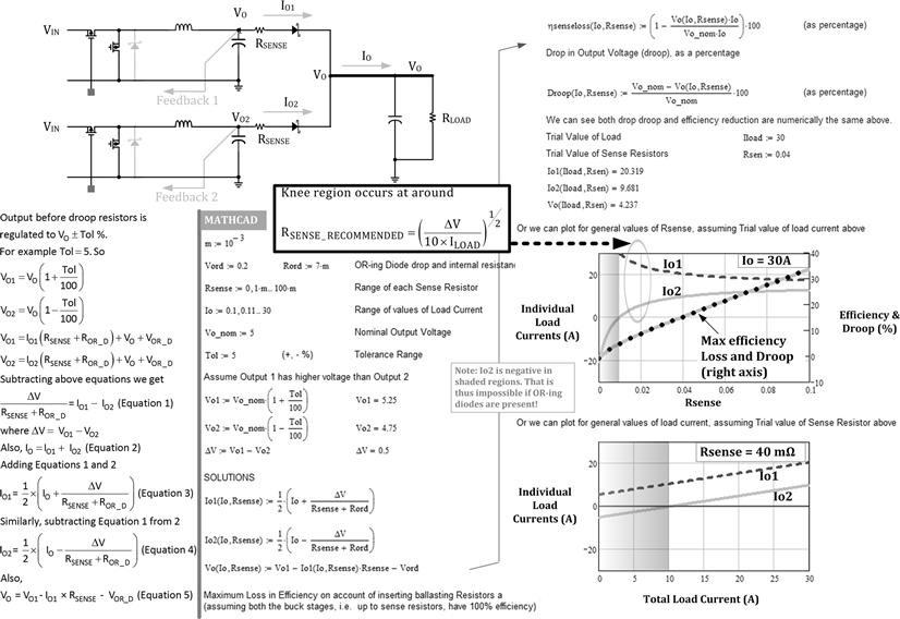
Figure 13.17: The droop method of paralleling power converters (passive load sharing).
Note that this is an eyeballed equation — based on an initial estimate of how far apart the output voltages of the two converters can possibly be (worst case). For example, if we are holding in our hands a 5 V at 5 A module with a possible tolerance range on the output anywhere from 4.75 V to 5.25 V, the possible ΔV is as large as 0.5 V for a nominal 5 V. We will usually need a really large (and impractical) droop resistor to parallel such modules. A better option is to manually trim the outputs of such paralleled converters so that they are brought very close to each other, and then we can depend on much smaller droop resistors to equalize their currents. Without that, passive sharing methods are inefficient and not very useful or practical.
A side note: yes, with current-mode control as discussed in Chapter 12, passive current sharing is much better since current is already being monitored cycle-to-cycle (though internally in the IC) as part of standard current-mode control implementation. But we do need to sense current in each converter. Also, the use of transconductance op-amps as the error amplifier of the feedback loop helps load sharing significantly, as compared to conventional voltage-based op-amps. The reason is when using transconductance op-amps, the feedback loop is completed externally, not locally. Locally means directly from the output of the error amp to its input pins, rather than through the converter. This was explained in Figure 12.12 and its related section. So, such op-amps are not so prone to “rail” just because of a small voltage difference on their input pins. In fact several transconductance op-amps belonging to multiple power-trains can be tied together at their inverting input pins without causing major issues. Transconductance op-amps are therefore recommended in droop-based (passive) load-sharing applications.
Active Load Sharing
With so many myriad causes responsible for unequal sharing, we can’t afford to tackle each cause separately. But what we can do is (a) look out for the symptoms of unequal sharing, and (b) correct by brute-force. That means we need to monitor the current in each module constantly, compare it with the others, and if sharing is not so good, we can then try to enforce it by tweaking the actual duty cycle of the guilty module. And that in turn is done by tweaking the reference voltage of that module. We realize we need to share current sense information between modules, so each module can realize if it is running “too wide” compared to the others. We also hope to do all that with just a “single wire” running from module to module (of course all the modules share a common ground too because nothing electrical can really be over a single wire with no return path). And that takes us to the concept of a signal bus called the “load-share bus” — which is a common feature of most active load-sharing modules. There are many ways of implementing this feature. But let us start from a simplified diagram outlining the pioneering 1984 patent by Ken Small working at Boschert (subsequently called Computer Products Inc., then Artesyn Technologies, and now part of Emerson Electric). It is US Patent 4,609,828 we refer to. We have explained this in a very simplified way in Figure 13.18. The share bus represents the average of all the output currents of all the modules.
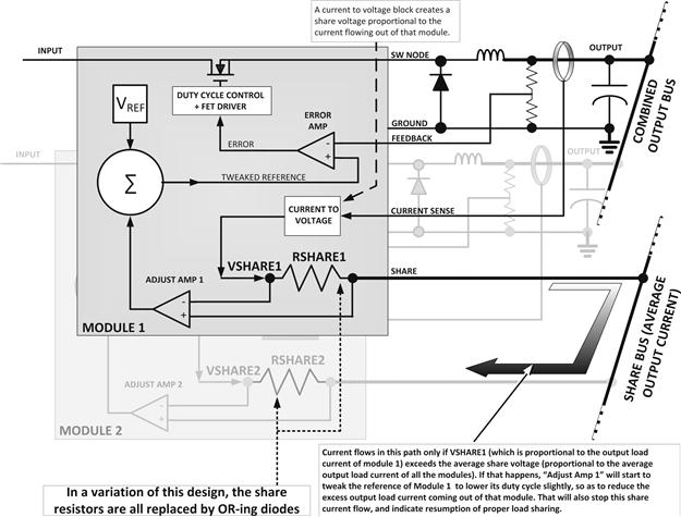
Figure 13.18: Active load sharing explained.
However, to avoid stepping on intellectual property, in a subsequent commercial variation of the original patent, two things were done: (A) the share resistor was replaced by a “share diode” and (B) the reference voltage was allowed to be tweaked only in an upward manner (i.e., increase allowed, no decrease). Now the share bus no longer represented the average of all the output currents of all the modules, but the output current of that module which is delivering the highest output current. Because sensed current is being converted to a voltage and then OR-ed through signal diodes (“share diodes”). Therefore, the module with the highest current will be the one to forward-bias its OR-ing signal diode, thereby also simultaneously reverse-biasing the other OR-ing signal diodes. The lead module thus automatically becomes a “Master.” Note that it becomes the Master primarily because its (unmodified) reference happens to be the highest of all the other modules. This is what happens to make it a Master. Its share diode is the first to conduct, causing a 0.6 V difference at the input pins of its adjust amplifier, forcing the output of the adjust amp low. That would leave the reference of the Master unaffected, because as mentioned, in this case the reference is allowed only to be adjusted higher, not lower, and we already know that the Master has the highest reference voltage to start with. That is exactly what we want, because the module that is forward-biasing its share diode is already providing the highest current, and we want to retain it as the Master to avoid constant “hunting” and any resulting unstable behavior. Note clearly that the voltage on the share bus is actually always 0.6 V (diode drop) below the share voltage coming out of the Master.
We recognize that the basic change in replacing share resistors with share diodes as in going from the original patent to its commercial variants, leads to a Master–Slave configuration. By means of the reverse blocking property of the share diode, this comes in handy if one module fails. In a typical fault condition in one module, the share voltage of the bad module falls, and therefore it automatically “drops out of the picture” without pulling down the entire share bus. The other modules can continue normal operation, and equally automatically they will “take up the slack” with a new Master being automatically appointed. This of course assumes each module has enough headroom in its basic power capability to be able to take up the slack.
Coming back to normal operation (no fault), we note that though the other modules (Slaves) follow the lead of the Master, they never quite get there. Ultimately, they all reach a mutually identical share voltage, but that voltage is still exactly one diode drop below the Master’s share voltage. This is how it happens. Since their share diodes are initially reverse-biased, the outputs of their adjust amplifiers are all initially forced high. This causes their reference voltages to be tweaked higher and higher, so they start driving more and more output current on to the combined output bus. The process continues exactly to the point at which their share voltages become exactly equal to the voltage present on the share bus. At that moment their reference voltages can no longer be tweaked any higher by design. However, note that the share voltage from the Master is still 0.6 V above the voltage on the share bus, which by now exactly equals the share voltage from all the Slaves. So, there is an inherent error during steady state operation — a small mismatch between the Master’s output current and of all the others. The Master will always end up pushing more current than the others. This inherent error in terms of current is basically 0.6 V divided by the actual voltage present on the share bus, because sensed voltage is proportional to the sensed current.
To minimize the above error, the Unitrode IC UC1907/2907/3907 ICs went a step further. Using some clever circuitry, they effectively canceled out the forward diode voltage drop of the share diode. In effect we have a “perfect signal diode” — it reverse-biases when expected, forward-conducts when required, and has zero forward drop. In principle, this reduces the error completely, and perfect load-sharing results. But actually, only on paper! In practice, slaves that have coincidentally similar (and slightly higher) reference voltages will constantly start fighting to become the Master. Therefore, to avoid constant hunting, a 50 mV offset was deliberately introduced in the UC1907/2907/3907 ICs. In effect, now, instead of a diode with 0.6 V drop, or a diode with zero forward drop, we have a diode with a 50 mV forward drop. This retains all the advantages provided by replacing share resistors with share diodes, and (almost) none of the disadvantages. Which explains why the Unitrode (Texas Instruments now) load-share ICs became the work-horse of the entire load-share industry for decades. For example, the UC 3907 is still in production at the time of writing and is not obsolete. But besides its existence, a family of similar parts has also evolved from it.