
Chapter 16
Practical EMI Line Filters and Noise Sources in Power Supplies
This chapter discusses typical line filters for suppressing conducted EMI emanating from power supplies. It goes into IEC safety aspects when selecting Y-capacitors and also discusses ways to maximize the effectiveness of components used in line filters, including the pros and cons of ground chokes. It discusses the origins of differential-mode and common-mode noise in switching power supplies and describes their EMI spectra and equivalent LISN models. Ways to chassis-mount semiconductors with minimal impact on EMI are also discussed, along with efficacy of the LISN itself at different frequencies.
Part 1: Practical Line Filters
Having understood common-mode (CM) and differential-mode (DM) noise concepts in Chapter 15, we can look at the overall strategy for designing conducted-mode EMI filters. We will focus mainly on filters for off-line (AC–DC) power supplies. However, several of the tips will be obviously applicable to DC–DC converters too.
Safety issues, thermal issues, and even loop stability concerns are intricately linked to the issue of EMI filter design. Particularly in designing EMI filters for off-line applications, safety becomes a major concern because the voltages are high enough to cause injury. We will briefly cover that aspect first.
Basic Safety Issues in EMI Filter Design
The concept of safety (as per IEC 60950-1), and how it impacts the filter section are explained rather simplistically in the following steps.
• Any exposed metal (conducting) part (e.g., the chassis or output cables) is capable of causing an electrical shock to the user. To prevent a shock, such parts must be earthed and/or isolated from the high-voltage parts of the power supply in some way.
• No single point failure anywhere in the equipment should lead the user to be exposed to an electrical shock. There should be two levels of protection, so if one gives way, there is still one level of protection available. That is the basic premise underlying safety: the probability of two unconnected/independent faults occurring at the same point and at the same instant is considered negligible.
• Levels of protection that are considered essentially equivalent are (a) earthing of the exposed metal surface, (b) physical separation (typically up to 4 mm) between any exposed metal and parts of the circuit containing high voltage, and (c) a layer of approved insulator (or dielectric) between any exposed metal and the high voltage. Note that in (c) this (single-level protection) insulator/dielectric must have a minimum dielectric withstand capability of 1,500 VAC or 2,121 VDC.
• To qualify the above slightly — connecting the metal enclosure of the equipment to Earth is not always considered an acceptable level of safety and protection, simply because earthing may still not be guaranteed. For example, the wiring of older houses may not even contain an Earth wire inside the common household power outlet. However, assuming for now that earthing is acceptable, we then need one more level of protection as per the safety concept. This could be “4 mm” of separation for example (IEC 60950-1 provides tables for knowing exactly how many millimeters are required, and where). But consider the case of a high-voltage MOSFET (switch) mounted directly on the (earthed) metal enclosure (say, to provide better heatsinking). We obviously can’t provide “4 mm” of physical separation in this case (between the MOSFET and the earthed enclosure). So, now we need to place one layer of approved insulator between them. In this position, the insulator is said to serve as “basic insulation.”
• If earthing is not considered acceptable to be recognized as a valid level of safety, or if we are dealing with equipment with a two-wire AC cord (no Earth wire), then, besides the layer of basic insulation, we need an additional level of protection between exposed metal (e.g., output leads) and high voltage (AC). This could be another insulating layer, with identical dielectric withstand capability. It is then “supplementary insulation.” Together, the two layers (basic+supplementary) are said to constitute “double insulation.” We could also use a single layer of insulation, with dielectric withstand properties equivalent to double insulation (i.e., 3,000 VAC or 4,242 VDC). That would then be called “reinforced insulation.”
• Why do we connect the enclosure to Earth in the first place, if that is not always acceptable from a safety standpoint? The main reason for earthing a metal enclosure is that we want to prevent radiation from inside the equipment from spilling out. Without a metal enclosure, there is very little chance that a typical off-line switching power supply can comply with radiated-mode (and perhaps even possibly conducted-mode) emission limits. By earthing, the enclosure is held at a fixed potential and therefore forms an excellent shield around the power supply for meeting radiated emission limits. But the metal enclosure is also, rather expectedly, eyed by engineers as an excellent and fortuitous heatsink. So, in practice, power semiconductors are often going to be mounted on the enclosure directly (with appropriate insulation ratings as indicated above). However, by doing this, we also create leakage paths (resistive/capacitive) from the internal subsystems/circuitry to the metal chassis. And even if we ensure that these leakage currents (CM noise currents) are small enough not to constitute a safety hazard, they can present a major EMI headache. We realize that if these leakage currents are not “drained out” in some way, the enclosure will charge up to some unpredictable/indeterminate voltage, and will ultimately start radiating (a dipole, or an electric field source). That would clearly be contrary to the very purpose of using a metal enclosure. So, we really need to connect the enclosure to Earth, other than for safety reasons. We note that even if we didn’t have power devices mounted on the enclosure, there could be other leakage paths present from inside circuitry to the enclosure. And besides that, an unearthed enclosure would also inductively pick up and re-radiate the strong internal electric/magnetic fields.
• To help in diverting CM currents away, capacitors are often connected between various parts of the power supply and the earthed enclosure (or earth terminal). These are called “Y-capacitors” or Y-caps. Similarly, to reduce DM currents, high-voltage capacitors are often placed between L and N of the incoming AC mains. These line-to-line components are called “X-capacitors” or X-caps. All Y-capacitors on the Primary side of an AC–DC power supply must be rated for a certain minimum voltage as discussed later. And, of the Y-caps on the Primary side, those that are before the bridge rectifier (i.e., on the line side) also carry low-frequency AC, and therefore safety agencies in effect regulate their total capacitance value. We will discuss this later.
• The bottom-line is that (a) providing a good metal enclosure and (b) properly connecting it to Earth are the most effective methods of preventing radiated EMI. However, by creating this galvanic connection (to Earth), we also now provide a “freeway” for conducted (CM) noise to flow “merrily” into the wiring of the building. So, in trying to suppress radiated EMI, we might end up increasing the conducted EMI, and vice versa. We thus realize that to be able to stay within the applicable conducted emission limits, we now need to provide a conducted EMI (CM noise) filter somewhere. Such are the reasons why, in Chapter 15, when we first introduced the topic of EMI, we had warned that EMI is a veritable balloon — push it in on one side only to find it bulging out on the other.
• Generally speaking, if the equipment is designed not to have any Earth connection (e.g., a two-wire AC cord), there will usually be no metal enclosure present either. Ignoring the problem of meeting radiation limits for now, the good news here is that no significant CM noise can be created either — simply because CM noise needs an Earth connection by definition. Therefore, a CM filter need not be present in this case. However, we must remember that conducted noise limits include not only CM noise, but DM noise too. So, irrespective of the type of enclosure and earthing scheme, DM filters are always required.
• In plastic enclosures, to comply with radiation limits, the inside of the plastic box may be shielded, say by an insulated wrap-around metal foil, or by depositing metal on its insides.
Four different coating processes are commonly used, each with its strengths and weaknesses.
(a) Vacuum deposition: A metal (e.g., aluminum) is melted in a vacuum chamber and its droplets sputtered onto the inner surface of the enclosure, gradually building up a continuous metallic layer. This process is ideal when very thin coatings are required on relatively detailed moldings. It is less effective if used on an enclosure with poorly fitting joints because the thin metal layer does not provide gap-filling properties, making electrical continuity difficult to maintain. Therefore, RF leakage around joints and seams is a real problem. Tooling costs are also high because only very precise masks and fixtures will ensure that metal is applied to only the inner surfaces of the enclosure.
(b) Loaded paints: This is the most cost-effective method. A silicone rubber shields the external surfaces, and the metallic-loaded paints are applied using a wet spray process using either an automated or a manual setup. A finished coating thickness of 50–75 μm gives good coverage without obliterating fine details of the molding. Copper- or silver-loaded paint is suitable for most applications requiring commercial levels of attenuation.
(c) Zinc arc spray: This results in a relatively thick layer over the molding surface. It is very effective in applications where a high magnetic field is expected, because of the direct relationship between material thickness and signal absorption. However, this process involves elevated temperatures, so it is most suitable for use with polycarbonate enclosures. The thickness of the coating can also obliterate fine details of enclosure molding.
(d) Electroless plating: This produces the best performance, but it is very expensive and not particularly suitable for high-volume applications. Masking is very difficult, and the screening material can easily get deposited on both the internal and the external surfaces. Further, a secondary finishing operation is required to remove the excess material and perhaps to apply a final painted-over finish. But since colors are intrinsic to the materials used in plastic enclosures, the secondary paint operation is a major disadvantage. All this gets complicated and costly. Therefore, this method is justified only in applications where high attenuation levels are the overriding concern.
Safety Restrictions on the Total Y-Capacitance
Y-caps don’t just let high-frequency noise pass through. If positioned before the bridge rectifier, they also conduct some of the low-frequency line current. This AC-related leakage current flows into the protective Earth/chassis where a person may contact it, providing an involuntary path to ground, at obvious risk to personal health. Therefore, safety agencies limit the total RMS current introduced into the Earth by equipment to a maximum of 0.25 mA, 0.5 mA, 0.75 mA, or 3.5 mA, depending on the type of equipment and its “installation category,” that is, its enclosure, its earthing scheme, and its internal isolation. In general, 0.5 mA seems to have become the standard value for most off-line power supplies. However, allowing higher leakage current allows for higher Y-capacitances, and thereby smaller CM chokes. So, it may be worth investigating if we can increase the earth leakage current above the so-called default value of 0.5 mA.
We can calculate how much leakage current we get per nF of Y-capacitance. The reactance of a 1-nF cap is
![]()
![]()
Every nF gives 79 μA at 250 VAC/50 Hz. This gives us a maximum allowed capacitance of 500/79=6.4 nF for 0.5 mA. Note that this is the sum of all the Y-capacitances present on the board (before the bridge rectifier). For example, in a typical two-stage EMI filter, we will often find four Y-caps, each one being 1 nF. This totals 4 nF. We can increase all the Y-caps to 1.2 nF, and we will still comply with the 0.5-mA limit. However, if we use four 1.5-nF caps, we may be in trouble if we are using caps with ±20% tolerance. Because we could then get a total lumped Y-capacitance of 1.2×4×1.5=7.2 nF, which will give us an earth leakage current of 7.2×79=569 μA, which exceeds the limit of 500 μA. Yes, we could use only two Y-capacitors, each of value 2.2 nF.
Besides a formal Y-capacitor, we may have earth leakage currents injected from high-frequency CM noise currents passing through small parasitic caps elsewhere on the board. These should also be accounted for in computing the total ground leakage current, and thereby correctly selecting the Y-caps of the line filter. In general, if a Y-cap is connected from the rectified DC rails to Earth (or from the output rails to Earth), there is no significant AC-related earth leakage current through these capacitors, so we can usually use much larger Y-caps in such locations.
Practical Line Filters
We now look at a typical power supply line filter, as shown in Figure 16.1. Its ultimate purpose is to control conducted emissions in general, and therefore it has two discernible stages — one for DM and one for CM. Let us make some relevant observations:
• Both the CM and DM stages are symmetrical (balanced). From the viewpoint of the noise emerging from the bridge rectifier and flowing towards the LISN, there are in effect two LC filters in cascade (both for DM and CM noise). This filter configuration can provide good high-frequency attenuation (roll-off). We know that any LC filter provides 40-dB/decade attenuation, so two in series can, in principle, provide up to 80 dB/decade.
• Typical practical values for the inductance of a CM choke in medium-power converters range from 10 mH to 50 mH (per leg). The large values result because we are limited by safety considerations in the amount of total Y-capacitance we can use. On the other hand, there being no similar concern for DM noise, the DM choke is always much smaller (in inductance, but not necessarily in size as we will see). Typical values for the DM choke are 500 μH to 1 mH.
• The leakage inductance of the CM choke Llk acts as a DM choke, albeit one with a rather small inductance. The leakage inductance of the CM choke is roughly 1–3% of Lcm, depending on its construction. That can serve as an unintentional, but effective DM choke.
• However, since the capacitance associated with a DM filter can be very large, and is not restricted by safety concerns, low-power flybacks (up to 70–80 W) rarely even use a discrete DM choke. Instead they usually have two CM chokes in cascade, relying on the leakage of each to provide DM noise filtering.
• If the chosen CM choke is toroidal in shape rather than a U-core or E-core, it will have almost no leakage inductance. In that case, we would most likely need to provide discrete DM chokes to create a DM filter.
• In Figure 16.1, we have shown both the CM and the DM filter stages as being symmetrical (balanced). For example, we have placed identical DM chokes on each of the L and N lines. However, the DM choke is also a part of the CM equivalent circuit as we can see from the CM equivalent circuit. As mentioned in Chapter 15, since line impedance imbalance can cause CM noise to get converted into DM noise, it is generally advised to keep both the CM and DM stages symmetrical (balanced).
• Occasionally, unbalanced DM filters provide acceptable overall EMI scans — for example, a single DM choke placed on one line only. It is worth trying out for sure. Sometimes, in very low-power applications, or in the case of DC–DC converters/bricks, a plain decoupling capacitor (e.g., C1) may suffice too. Tuned filter stages are also sometimes seen in commercial off-line power supplies (e.g., from Weir Lambda, UK). But there are some anecdotal industry experiences that suggest that under severe line transients or under input surge waveforms, as those typically used for immunity testing, tuned filters can display unexpected oscillations (resonances), ultimately provoking failure of the power supply itself. Therefore, tuned filters are usually avoided in commercial designs.
• One obvious way to maintain equal CM inductances in both lines is to wind them on the same core (e.g., a toroid). That automatically assures a good inductance match (assuming of course that there are an equal number of windings per leg). Note that if we are winding the CM choke ourselves (as during prototyping), we must note the relative direction of the windings, as indicated in Figure 16.1 (see the embedded third and fourth sample CM choke pictures from the left). With such a winding arrangement, the magnetic field inside the core will cancel out completely (in principle) for DM noise. For the same reason, the flux due to the operating AC line current will also cancel out (that too being differential in nature). Therefore, the CM choke will be basically “visible” only to the CM noise component. This choke does not need to be “large” based on DC-bias considerations, but in reality, is in fact quite bulky — due to the high inductance required, and because of the associated large number of turns (all rated for the AC operating current).
• While winding toroidal CM chokes, we need to keep other safety requirements in mind too. We cannot simply wind the two windings carelessly overlapping each other — we need to maintain a specified physical separation between the windings of each AC phase. Nor can we just use a bare ferrite toroid to wind them on because ferrite can be a rather good electrical conductor. Neither should we rely on the enamel coating of a typical copper magnet wire as it is typically not a safety-approved coating. What we really need is a safety-approved coating for the toroid and/or a suitable bobbin.
Note: The reader is cautioned that there are several widely used but confusing symbols for the CM choke existing in schematics found in related literature. Whatever the symbol, as long as it is meant to serve as a CM choke, the direction of the windings must be as in the embedded toroid pictures in Figure 16.1. The correct winding polarity is also indicated by dots in the same figure.
• We should also keep in mind that in theory, the AC operating current flux cancels out in the CM choke. In reality, on account of small imbalances in symmetry of the windings the choke could “topple over” (i.e., progressively flux-staircase over toward one side). This would expectedly degrade the EMI performance, but in extreme cases, the core may even saturate. Though that is not a catastrophic event, it still needs to be fixed since the filter is likely no longer EMI-compliant. Sometimes we may need to oversize the CM choke, just to give it a higher-than-zero DC-bias rating. We may also need to provide some air gap. This may be an actual air gap (between split halves), or it may be a distributed gap, as in powdered iron cores. See Chapter 5 for a better understanding of air gaps and why they help smoothen out production tolerances in core materials and magnetic assemblies. But all such steps do lead to an increase in size of the choke.
• The inter-winding capacitance of a choke affects its characteristics significantly at high frequencies. This can be intuitively visualized as an AC path providing an easy detour for noise to flow past the windings rather than through them. To minimize the end-to-end capacitance of a toroidal winding, it is recommended that the winding be single layer. Coming to U-core type of CM chokes, in Figure 16.1, the sample CM choke picture second from the left is better than the one to its left, in terms of minimizing end-to-end capacitance. That is because of the split introduced in each winding section by the special bobbin used. The split also helps increase the leakage inductance (which helps reduce DM noise). CM choke bobbins with multiple splits are also available, at a higher price of course.
• If we reverse the current (or winding) direction in one of the windings of a CM choke, then it becomes a DM choke (for both lines). However, now it is also subject to the flux produced by the AC line input current (no flux cancellation occurs). Therefore, DM chokes, in general, should always be put through a “core-saturation check.” We may see that DM chokes may need to be quite large, just to avoid core saturation — despite the fact that their inductance is usually much less than that of CM chokes. See Chapter 14 for the peak currents in the input lines. That should help ensure the DM choke is really effective.
• We can consider spending some more money and avail of magnetic materials like “amorphous” cores or “Kool Mu®” if we want to achieve higher inductance (with higher saturation flux densities) in a smaller size.
• Note that the EMI filter stage is usually placed before the input bridge (i.e., toward the incoming AC line input) — because in that position it also suppresses any noise originating from the bridge diodes. Diodes are known to produce a significant amount of medium- to high-frequency noise, especially at the moment they are just turning OFF. Small RC snubbers (or sometimes just a “C”) are therefore often placed across each diode of the input bridge. Though sometimes, we can get away simply by choosing diodes with softer recovery characteristics.
• Note that input rectifier bridges using ultrafast diodes are often touted as offering a significant reduction in EMI. Opinions about them remain mixed. Some people claim that with these ultrafast diode packs, it is possible to remove the small ceramic capacitors often placed across the four diodes of a typical bridge rectifier. However, in actual tests conducted by the author, the ultrafast diodes didn’t seem to make much difference. If anything, the conducted EMI spectrum actually worsened. We know that very fast diodes can have very “snappy” characteristics too, producing rather sharp spikes of reverse current and forward voltage at turn-off and turn-on, respectively. And that could explain the rather poor results with them.
• Line-to-line capacitors (the X-capacitors or “X-caps”), placed before the input bridge, must be safety approved. After the bridge (i.e., on the rectified side), it’s basically a “don’t care” situation from the safety point of view. At that position, we can use any suitably rated cap really. Note that since an approved X-cap is essentially a front-end component, it can see rather huge voltage spikes coming in from the AC mains. For example, the voltage spikes could be from motorized equipment connected to the same wiring, turning ON and OFF repeatedly. That is why an approved X-cap, even though rated “250 VAC,” is actually 100% impulse-tested up to 2.5-kV peak.
• Line-to-earth capacitors, or “Y-capacitors,” as discussed previously, used anywhere on the Primary side (in an off-line application) must always be safety approved. Any Y-cap placed as a bridging component from anywhere on the Primary side to anywhere on the Secondary side must be safety approved. Since Y-caps are critical in terms of having the potential to cause electrocution if they fail, approved Y-caps are typically impulse-tested up to 5-kV peak. They should also be guaranteed to fail open, not shorted. Depending on the equipment’s expected region of operation, some safety agencies (e.g., in Scandinavian regions) may require us to assume no earthing is present, and therefore we will need to create two levels of protection, by placing two Y-caps in series (basically corresponding to double insulation).
• Note that Y-caps placed between the Secondary side and the Earth/enclosure are often just standard (non-approved) 0.1-μF/50-VDC ceramic capacitors. Sometimes, the low-voltage (<60-V) outputs can even be directly connected to the enclosure. Safety agencies don’t care. However, if the power supply is intended to provide the 48-V rail in PoE (Power over Ethernet) applications, by IEEE requirements, we need to provide 1,500-VRMS (~2,500-VDC) functional isolation between Earth/enclosure and the 48-V output rail plus its return. The reason is that severe voltage spikes may be picked up by the cables carrying data and power across the building. And if we connect those directly to the enclosure, we can cause the user an unpleasant (though not fatal) shock. So, in off-line power supplies meant for telecom applications in general, we cannot use low-voltage Y-caps on the outputs anymore. To support PoE, we therefore use either approved or nonapproved 2.5-kV-rated Y-capacitors on the outputs.
Note: What were traditionally called X- and Y-capacitors are more accurately “X2” and “Y2” capacitors respectively. Historically, X2 and Y2 caps were meant for single-phase equipment, whereas X1 and Y1 caps were meant for three-phase equipment. From the viewpoint of safety regulations (like impulse voltage rating and so on), X1 and Y1 caps are considered equivalent to two X2 and Y2 capacitors in series respectively. Therefore, for example, Y1 caps are typically 100% impulse-tested to 8 kV (Y2 caps to 5 kV). We could use Y1 caps for meeting Scandinavian safety deviations.
• Traditionally, off-line X-caps were of special metallized film+paper construction, whereas Y-caps were a specially constructed disc ceramic type. However, we can also find X-caps that are ceramic, as we can find Y-caps which are film type. It’s a choice dictated by cost, performance, and stability concerns. Film capacitors are known to always provide much better stability over temperature, voltage, time, and so on — than most ceramics. In addition, if they are of “metallized” construction, they also possess self-healing properties. Note that ceramic capacitors, in general, do not have any inherent self-healing property. However, ceramic caps used as approved Y-caps are specifically constructed in such a way that they will not fail shorted under any condition.
• If for any reason (e.g., filter bandwidth or cost), ceramic is preferred for a Y-cap position, then we need to carefully account for its basic tolerance, the variation of capacitance with respect to temperature and applied voltage, and all other long-term variations and drifts. That is because we need a certain filtering efficacy over the life of the product. But at the same time we can’t increase the leakage current into the chassis or we will violate ground leakage current limits. We should therefore keep in mind that the capacitance value stated in the datasheet is not just a nominal (or typical) value, but in fact can be a rather misleading value. For example, the fine print may reveal that the test voltage at which the capacitance is stated is close to, or equal to, zero volts. So, the actual capacitance value the capacitor presents in a real working circuit may be very different from its declared (nominal) value. This is, in general, especially true for ceramic capacitors which use a high dielectric constant (“high-K”) material (e.g., Z5U, Y5V, etc.). We should also know that ceramic capacitors age slowly, except for COG/NP0 types. But COG/NP0 capacitors are very expensive and bulkier too. A typical X7R capacitor ages 1% for every decade of time (in hours). So, its capacitance after 1,000 h will be 1% less than what it was after 100 h, and so on. Higher dielectric constant ceramics like Z5U can age 4–6% for every decade of time. So, in effect our filter stage too gets less effective with time. And we need to account for this upfront, in the initial design.
• Theoretical filter performance is based on the assumption that we are using “ideal” components. However, real-life inductors are always accompanied by some winding resistance (DCR) and some inter-winding capacitance. Similarly, real capacitors have an equivalent series resistance (ESR) and an equivalent series inductance (ESL). At high frequencies, the inductance will start to dominate, and so a capacitor will basically no longer be functioning as one (from the signal point of view). However, capacitors with smaller capacitances generally remain capacitive up to much higher frequencies than do larger capacitances. See Table 16.1 for some typical self-resonant frequencies (the point above which, capacitors start becoming inductive). Therefore, quite often, a smaller Y-cap may help in situations where a larger Y-cap is not yielding the required results. We can also consider paralleling a larger value Y-cap with a small Y-cap.
• Surface mount (“SMD”) versions of off-line safety capacitors are available — for example from Wima in Germany and Syfer in UK. But especially for SMD caps, we must keep in mind that it is not enough for a manufacturer to spontaneously declare their capacitor “complies” with a certain safety standard — the capacitor should actually be approved. Only after being tested by various safety agencies, is it allowed to carry their respective certification marks. From the electrical point of view, one of the great advantages of SMD caps is their very low ESL. This improves their high-frequency performance in any filter application.
• Note that in the relentless drive toward reducing parasitics, we may forget that some ESR or DC winding resistance (“DCR”) is often useful in helping damp out oscillations. Without any resistance to burn up the energy, oscillations will last forever. That is one of the reasons why engineers sometimes pass one or both of the leads of a standard through-hole Y-cap through a small ferrite bead (preferably of a material with lossy characteristics, like Ni–Zn). This can often help suppress a particular high-frequency resonance involving the Y-cap that is perhaps showing up in the conducted EMI scan. But we must be careful that in doing so, we do not land up with a radiation problem instead.
• Designers of low-voltage, low-power DC–DC converters may find the “X2Y” patented product range available from Syfer (and from the company X2Y itself) useful if they need to miniaturize and lower the component count. This is a three-terminal integrated SMD capacitor-based EMI filter that simultaneously provides line-to-line decoupling and also line-to-ground decoupling. From X2Y’s website quoted verbatim: “The patented X2Y® Technology consists of proprietary electrode arrangements that are embedded in passive components. Components with X2Y technology can be manufactured in a variety of dielectric materials including ceramic, metal oxide varistor (MOV), and ferrite. The main embodiment of X2Y Technology is in a multilayer ceramic capacitor, this allows capacitor manufacturers to license X2Y. End-users can then purchase X2Y® components just as they would any other passive component. Currently, there are six licensed manufacturers who make and sell X2Y components.”
• Picor (a subsidiary of Vicor) sells active input EMI filter stages for standard 48-V bricks and off-line power supplies. These are expensive (typically ~$50 per unit), but may be a viable choice if board space is at a premium.
• We note that a Y-cap is always tested to higher safety standards than an X-cap. So, we can always use a Y-cap at an X-cap position, but not vice versa. For example, we can consider placing a ceramic Y-cap in parallel with a film X-cap to improve the DM filter bandwidth. However, nowadays, to keep things simple, manufacturers are selling safety approved caps designated for use either as an X-cap or a Y-cap.
• We often run into the problem of needing to improve filter performance in the low-frequency region of the CISPR-22 Class B limits. We do this by trying to increase the “LC” product as much as practically possible (in the process, lowering the resonant frequency). Given a choice, we would prefer to realize the large target value of the LC product, by using larger capacitances instead of impractically sized inductors. But as we know, the total Y-capacitance (before the bridge rectifier) is limited by safety considerations. Note that X-caps too seemed to be limited for many years to a maximum value of 0.22 μF, or occasionally 0.47 μF. But that was actually based on availability and component technology limitations. Nowadays, we can get approved X-caps up to 10 μF. We should, however, be conscious that large input capacitances can cause undesirably high inrush surge currents at power-up. This may also cause eventual failure of the X-cap, especially if it is the very first component after the AC input inlet. The X-cap may not fail outright since we know that film caps can self-heal from such events. However, eventually, the capacitance will degrade over time. Therefore, despite EMI concerns, we should try to place X-caps after any input surge protection element, for example, after the NTC (negative temperature coefficient) thermistor, or a wirewound resistor, perhaps even after a front-end choke.
Table 16.1. Practical Limitations in Selecting Components and Materials for EMI Filters.
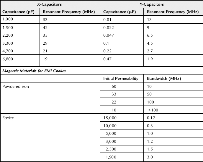
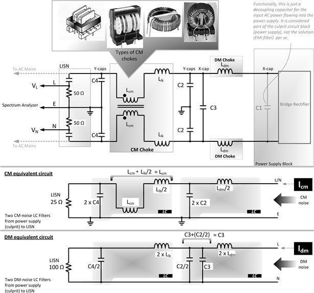
Figure 16.1: Practical line filter and the corresponding CM and DM equivalent circuits.
Examining the Equivalent DM and CM Circuits and Filter Design Hints
The filter in the upper part of Figure 16.1 reduces to the CM and DM equivalents shown in the lower part of the same figure. Note that C2 and C4 are small (being Y-caps), but C3 is large. Some observations are:
CM filter: We see that the discrete DM choke Ldm acts as a CM filter element too. The CM filter stage consists of two LC stages. One stage has a large LC product (low-frequency pole) corresponding to the product 2×Lcm×C4. The other provides high-frequency filtering since its LC product is relatively small: Ldm×C2.
DM filter: We see that the CM capacitor (C4) acts as a DM filter element too. The DM filter stage consists of two LC stages. One stage has a large LC product (low-frequency pole) corresponding to the product 2×Ldm×C3. The other provides high-frequency filtering since its LC product is small: Llk. Note that if we use a toroidal CM choke, this high-frequency DM filter stage may barely exist since Llk will be almost zero.
Though CM chokes usually have a high inductance (and that is certainly needed — particularly for complying with CISPR-22 limits below 500 kHz), a good part of CM noise is usually found in the frequency range of 10–30 MHz. So, we must consider the fact that not all ferrites have sufficient bandwidth to be able to maintain their inductance (AL) at such high frequencies. In fact, materials with a high permeability tend to have a lower bandwidth, and vice versa (“Snoek’s law”). Therefore, a “high-inductance” CM filter may look good on paper, it but may not be as effective as we had thought, at high frequencies. See Table 16.1 for typical values of initial permeability versus bandwidth (bandwidth being defined here as a 6-dB fall in permeability).
In the latter sections of this chapter, we will see that a DM noise generator is more like a voltage source. So putting in an LC filter works well for a DM source, as it presents a “wall” (mismatch) of impedance which serves to block the DM emissions from entering the mains. But a CM noise source behaves more like a current source. And we know that current sources demand to keep current flowing. They can surmount any “wall” of impedance by increasing voltage if necessary. Therefore, for dealing with CM sources, rather than try to only block CM noise from flowing into the mains, we should also close the current loop locally inside the power supply itself. Plus we should try to dissipate that energy rather than have it circulate constantly (or slosh back and forth). Only then would the CM filter stage as shown in Figure 16.1 really work. This is part of the pattern of nonintuitive behavior of inductors and current sources at large, as discussed in Chapter 1. This is also the point we start understanding why EMI issues in power supplies are so much different from those faced by signal integrity engineers.
To dissipate CM energy effectively, a “lossy” ferrite material for the CM choke often works well. The usual ferrite used for power transformers and inductors is of manganese–zinc composition. Lossy ferrites (using nickel–zinc) have higher AC resistance at high frequencies, so they can be more helpful in “killing” high-frequency CM noise components. Unfortunately, lossy ferrites also have very low initial permeabilities, so it is almost impossible to get the desired high inductance (as sorely needed to filter low-frequency noise). So, the functions are separated — one CM choke is used to “block” and another is introduced to “burn.” The latter CM choke’s inductance is not important anymore, so it could be just a small bead/toroid/sleeve made of lossy material, with both the L and N wires passing through it together. Many commercial power adapters, for example, have a big ferrite sleeve on their input AC cord.
Engineers are often mystified to find that making the DM choke out of (low permeability) powdered iron or lossy ferrite helps too, when all else has failed — despite all the talk about DM noise being essentially a “low-frequency emission” and so on. The reason is as follows — the CM noise in a power supply is actually mixed-mode (MM) noise at its point of creation (this will be discussed shortly). Though ultimately, by cross-coupling, it does tend to spread onto both lines almost equally. We had shown in Chapter 15 that MM noise can be considered a mix of CM and DM components. Therefore, in practice, we do get a fair amount of high-frequency DM noise too — arising out of the mixed-mode noise. That is why high-bandwidth/low-permeability/lossy materials often help in DM noise suppression too.
The DM and CM filters are often, but not always, laid out in the order shown in Figure 16.1. The CM filter stage is shown closest to the AC inlet. The idea is that the very last stage the noise encounters (as it travels from the power supply into the mains) should be a CM filter. Because, if, for example, this last stage was a DM stage, then if it was not very well balanced in impedance from the viewpoint of the noise emerging from the preceding CM filter, the CM noise could get converted into DM noise as previously explained. However, admittedly, many successful commercial designs have reversed the order shown in Figure 16.1. There seems to be no universally accepted rule for which stage should come before which one.
A possible location for an additional X-cap is directly on the prongs of the AC inlet socket (at the entrance to the power supply). We remember that in this position any line-to-line capacitor will be exposed to a huge current surge at power-up, and could degrade, if not fail immediately. So if this X-cap position seems to be the last resort, it should at least be made as small as possible (typically 0.047–0.1 μF). Or we can try ceramic capacitors in this position (approved ceramic X-caps or Y-caps can be tried here), since they have high surge current capabilities arising from the very low heat generated in them (due to very low ESR).
Similarly, the two front-end Y-caps (“C4” in Figure 16.1), or two additional Y-caps, can also be connected directly on to the prongs of the AC inlet socket, rather than on the PCB. This can help a great deal if the wires going from the PCB to the mains inlet socket are themselves picking up stray fields (radiation).
Sealed chassis mountable line filters (sometimes with integrated standard “IEC 320” line inlets) are available from several companies like Corcom (now part of Tyco Electronics) and Schaffner in Germany. Such filters perform well, but they are less flexible to subsequent tweaking, and also far more expensive than board-mounted solutions. Note that the performance of most commercially available line filters is specified with 50 Ω at both ends of the filter. Therefore, its actual performance in a real power supply may be quite different from what its datasheet says.
To prevent the enclosure from radiating, it is important to make a good high-frequency connection from the enclosure to the Earth terminal (the middle prong of the AC inlet). A thick wire (preferably braided) can be used to connect the two. Better still, standard AC inlets with built-in metal brackets can be used for the purpose. These are easily available nowadays, as from Methode Electronics. The connection from the CM filter on the board can be made to the AC Earth terminal via the enclosure. Metal standoffs can be positioned on the enclosure to provide mechanical stability and connect to the correct PCB traces on the EMI filter. However, since we want to prevent CM noise from entering the AC mains, making a good ground connection may serve the opposite purpose. However, if we don’t make a good connection to Earth ground, we may reduce the amount of CM noise directly thrown into the AC wiring, but we will have a major radiation problem instead. And that could easily convert itself into a conducted-mode EMI problem eventually, through radiated pickup. However, the ambivalence associated with the basic question of how “good” should the connection be from the midpoint of the two C2/C4 caps in Figure 16.1 to the Earth prong of the AC inlet has resulted in something called the “ground choke.”
The Ground Choke
We ask — is it really a good idea to insert a small inductor (e.g., a bead or small toroid with a few turns on it) on the wire connecting the on-board EMI filter to the Earth prong? This is called a “ground choke” or “Earth choke.” It is commonly found on low-power evaluation boards (from vendors promoting their integrated power IC solutions), but rarely seen on a commercial power supply. Why is that?
When we place the ground choke, we are basically trying to prevent conducted CM noise from flowing into the mains wiring. But in return, we may have a radiation problem. In addition to that, there are industry-documented cases where the ground choke has caused severe system problems. For example, if a power supply is suddenly connected to the mains at the peak of the input AC waveform, there is a high surge of current through its Y-caps too. If there is a ground choke present, it causes the voltage on the Earth traces and the enclosure to locally “bump up.” Now in some cases, the return of the output rails of the power supply is also connected directly to the enclosure, and forms the ground plane for the entire system. The system would also typically connect to the chassis/enclosure at several points downstream. So, this surge-induced bump, around the power supply, causes severe imbalances across the system ground plane — leading to data upsets and even destruction of the subsystems. A similar situation will arise during ESD testing and conducted immunity testing, in which surge voltages are applied from line to line, or from line to Earth. So, however, tempting it may seem to the power supply designer (who is focused only in solving his conducted-mode EMI problem) a ground choke should be avoided at all costs. Some high-voltage semiconductor companies, who are only making open-frame (enclosure-less/standalone) evaluation boards, seem to have nothing to lose, and everything to gain, by putting in a ground choke. Perhaps they know that being open-frame anyway, no one expects them to comply with radiation limits. So, they may just have pushed the problem from the conducted emissions plot toward a future radiation emissions’ saga for the systems designer.
Some Notable Industry Experiences in EMI Filter Design
One of the most stubborn cases of conducted EMI failure encountered by the author while working in Germany was ultimately (and rather mysteriously) solved by simply reversing the orientation of the CM choke (i.e., turning it by 180° on the PCB). It was later deduced that the leakage from the core was being picked up by a nearby trace or component, and so the phase of the coupling had somehow become an issue (interference pattern). But since most inductors/chokes are symmetrically built, and also do not carry any marking to distinguish one side from the other, implementing such a fix was not easy in production. However nowadays, with so many similar “orientation-sensitive” cases being reported (even relating to the main inductor of the converter itself), some key inductor manufacturers have taken the step of placing a “polarity mark” on their inductors/chokes.
In another well-documented EMI problem at a leading power supply manufacturing house, it was discovered that the CM choke had to be rotated by 90° (not 180°) to achieve compliance. That clearly spells “bad news” if the unit is already in production, because it means the PCB layout has to be redesigned (and perhaps the power supply needs to be requalified too).
Part 2: DM and CM Noise in Switching Power Supplies
Main Source of DM Noise
Now we turn our attention to a real power supply to see for ourselves where all the buzz is really coming from. First consider what would happen if the input bulk capacitor of the power supply had been a “perfect” capacitor, that is, with zero effective series resistance (ESR) (ignoring all other capacitor parasitics too). Then any possible differential noise source inside the power supply would be completely bypassed/decoupled by this capacitor. Clearly, the reason this does not happen is the non-zero ESR of the bulk capacitor.
So, the ESR of the input capacitor is the major portion of the impedance “Zdm” seen by the DM noise generator (see Figure 15.6). The input capacitor, besides being refreshed by the operating current flowing in through the supply lines, also tries to provide the high-frequency pulses of current demanded by the switcher. But whenever current passes through any resistance, such as the ESR in this case, there must be a corresponding voltage drop. So, we will see a high-frequency voltage ripple across the terminals of the input capacitor as seen in Figure 16.2. The high-frequency voltage ripple shown in the figure is, in effect, the DM noise generator. It is essentially a voltage source (VESR_PP). In theory, this high-frequency ripple-related noise is supposed to appear on the left (input) side of the bridge rectifier only when the bridge is conducting. In reality, it may spill past the parasitic capacitances of the diodes of the bridge, during the OFF-time of the bridge too. In the next section, we will see that DM noise can also be generated when the bridge rectifier is OFF, but this time it appears as a current source, not a voltage source.
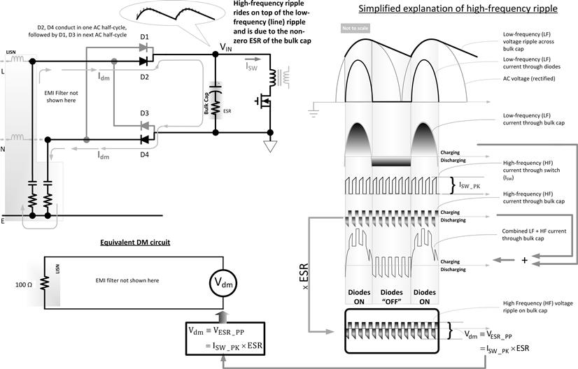
Figure 16.2: How DM noise is created.
The Main Source of CM Noise
Various inadvertent paths may be present carrying high-frequency current into the enclosure. A key culprit is shown in Figure 16.3. As the Drain of the FET swings high and low, current flows through the parasitic capacitance between the FET and the heatsink (the heatsink is connected to, or is, the enclosure in our case). We see that when the AC line current is holding the bridge rectifier ON (diodes D2 and D4 first ON, followed by D1 and D3 in the next AC half-cycle, and so on), the noise injected into the enclosure sees almost equal impedances (and voltages) and therefore flows equally on the L and N phases. So, it constitutes pure CM. However, when the bridge turns OFF, the noise forces (only) one diode of the bridge to turn ON, since the inductor current is behind the noise current too. However, this creates unequal impedances, and so the noise current does return, but through either the L or the N phase, not split equally between the two. As a result, as we have shown in Figure 15.6, this MM noise is in effect a pure CM noise component plus a very large, high-frequency DM noise component. The way to equalize the CM noise flow into both phases, and thereby reduce this contribution to the DM noise source, is to provide an X-cap right before the bridge. Any required EMI filter can be placed between this cap and the AC mains, as I have indicated in Figure 16.1 too.
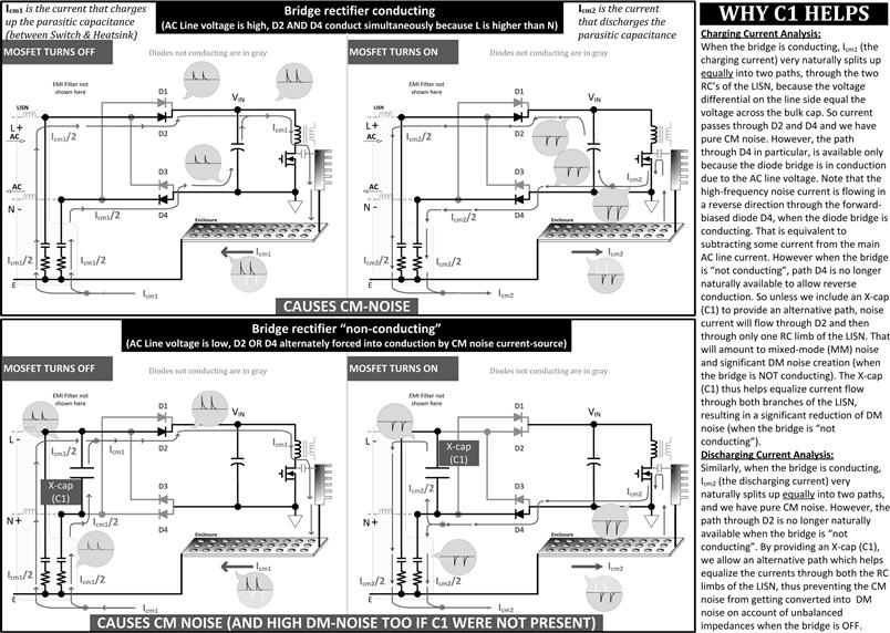
Figure 16.3: How CM noise is created.
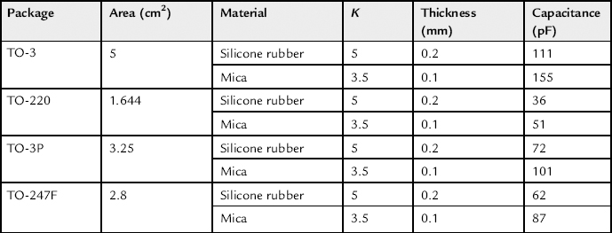
Typical values of parasitic capacitance that can be created in a power supply by the insulator are presented in Table 16.2. Here we are comparing a traditional insulator material, mica, with a modern choice, silicone rubber. K is the dielectric constant.
Table 16.2. Typical Mounting Capacitances.
Chassis-Mounting of Semiconductors
Even seasoned engineers are often extremely nervous about chassis-mounting of power devices. Often they can be coaxed into mounting the output diodes in this manner (since the diodes have lower voltages), but not the high-voltage FET. However, there is a way to do this. If the Y-cap shown in Figure 16.4 (marked “Y-cap”) is placed, along with a high-frequency ceramic cap across the bulk cap, together they will return the injected noise very close to the FET. Note that we need a metal standoff from the enclosure to the PCB very close to where the FET is mounted (PCB is not shown in the figure). Small current loops minimize radiated H-fields. So EMI is reduced. This is also a good place to insert a Ni–Zn ferrite bead somewhere in the path, to help burn up the circulating heatsink-injected noise energy.
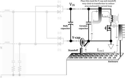
Figure 16.4: How to mount power devices on the enclosure.
The CM Noise Source
We were implicitly assuming by using the X-cap C1 in Figure 16.3, that we were dealing with pure CM noise, not MM noise. In Figure 16.5, we draw the exact injected current previously indicated vaguely in Figure 16.3. We have a current spike associated with the rising voltage edge and another spike coinciding with the falling edge. (This is just one way engineers model this; there are other treatments in literature, but yielding similar results.)
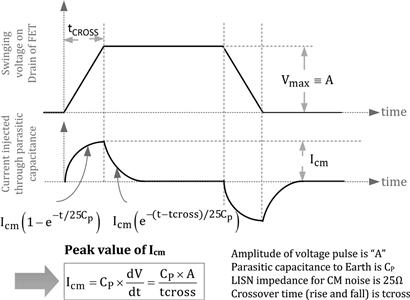
Figure 16.5: CM noise current injected through the FET-to-Heatsink mounting capacitance.
The shape of the current waveform in Figure 16.5 provides the entire harmonic content of the injected current. The measured noise at the LISN when t<tcross is
![]()
and for t>tcross it is (all this based on M.J. Nave’s paper in APEC 1989)
![]()
The same situation occurs when the FET turns ON — only the directions are reversed. We can do a Fourier analysis of the measured voltage waveform, and the result is (in frequency domain)
![]()
In Chapter 18, we will discuss Fourier series in greater detail. We will see that the sin x/x term (called the “sinc function”) always contributes an (additional) 20 dB/decade roll-off after the breakpoint which is located at x=1. Its value is close to unity till the breakpoint (i.e., for x<1). The term in the rightmost bracket above (involving the imaginary terms with j=√−1) has no roll-off. Its magnitude changes between the limits 0 and 2 as the harmonic number changes or/and duty cycle changes. So, for all practical purposes, if we are just interested in the envelope, we can take its maximum value of 2 to get the voltage picked up on the LISN.
![]()
This plot of Vcm is flat till the break frequency (x=1), after which it rolls off at 20 dB/decade. The flat part (the “pedestal”) can be found using the approximation sin x/x≅1 for small x. We thus get
![]()
For example, if A=200 V (amplitude of voltage on Drain of FET), CP=200 pF, fSW=100 kHz, we get
![]()
This is without an EMI filter. With a filter, we will need to provide a certain attenuation to bring it within the acceptable limits described in Chapter 15. A complete design procedure is provided in Chapter 18.
The Road to Cost-Effective Filter Design
In Chapter 18, we will see that the envelope of the switching harmonics falls off with a slope of −20 dB/decade as frequency increases. Alternatively stated, the harmonic amplitudes rise at the rate of 20 dB/decade as the frequency decreases. Note that by definition, that is, in effect, a 10-fold increase (20 dB) in amplitude of the harmonics every 10-fold decrease in frequency (decade). Looking at the CISPR-22 Class B EMI limits in Figure 15.2, from the dashed gray extrapolations, we see that from 150 kHz to 500 kHz, the CISPR limits allow for a 20-dB/decade increase in switching harmonics. The original purpose of that was to create an allowance for switching power supplies. However, by designing a typical one-stage low-pass LC filter for EMI, we find that its attenuation decreases at the rate of 40 dB/decade as the frequency decreases. In other words, it becomes less effective at lower frequencies. That is the reason it becomes imperative that we design the filter such that we are below the limits at the lowest frequency of interest (150 kHz, or the switching frequency of the converter, whichever is greater). Once we do that, as the frequency increases, the CISPR22 limit lines demand a 20-dB/decade reduction in harmonics as frequency increases toward 500 kHz. However, we get that automatically since the envelope of our switching harmonics also falls off at the rate of 20 dB/decade. But there are several factors affecting us here as described below.
(a) As the frequency increases, the LC filter becomes more and more effective, at the rate of 40 dB/decade. So, we get an additional advantage of 40 dB/decade over what the limits allow.
(b) The LISN sensitivity actually increases with frequency (see Figure 16.6). That will give higher readings as the frequency increases. It is, in effect, a disadvantage of 3.5–10 dB/decade depending on frequency.
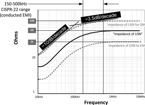
Figure 16.6: LISN impedance at low frequencies.
Together, from (a) and (b) above, we get a theoretical advantage of about 40−3.5=36.5 dB/decade as frequency increases. However, we are going to need that margin. As the frequency increases, the response of the filter is again going to worsen due to parasitics and ferrite bandwidth. Also, CM noise effects will start to dominate. In addition, conducted-mode readings will get affected by radiation pickup. There will also be some additional spikes in the EMI scan due to parasitics we didn’t model. Note that spikes should be dealt with individually at the board level, rather than try to bring the entire EMI spectrum down by a brute-force over-designed filter.
In general, it is important to be aware of the “trends” described above. In Chapter 18, we will do a formal EMI filter design. In effect, because we have “margin” at higher frequencies, the objective of filter design is to primarily achieve compliance at the lowest frequencies of interest. That is also the hardest to do. Which is why, compliance to FCC Part 15 Subpart B (at 450 kHz) is usually far easier than for CISPR-22 (at 150 kHz).