
Chapter 18
The Math Behind the Electromagnetic Puzzle
This goes into Fourier series and the resulting frequency spectra of typical differential and common mode noise sources in switching power supplies. Detailed numerical examples are presented in each case, for a top to bottom filter design.
Fourier Series in Power Supplies
In previous chapters we have seen that differential and common mode noise (DM and CM) emissions are basically either voltage or current sources with arbitrary waveshapes. What they have in common is that they are repetitive, and therefore involve the basic switching frequency of the converter. When we design a filter to suppress these emissions, we have to be conscious of the fact that the efficacy of a filter is best characterized in terms of the impedance it presents to a sine wave of a given frequency passing through it. In other words, to know the efficacy of the filter to CM and DM emissions, it is best to “decompose” the DM and CM waveforms into a sum of infinite sine wave components of varying amplitude and phase. As per the litmus test, when all the components are summed up, we should get back the original waveshape we started off with. The procedure of decomposition and reconstruction of an arbitrary waveform, either current or voltage, into sine wave components that are multiples of a basic (fundamental) frequency, is called Fourier series analysis. In general, we start with a “fundamental frequency” or “first harmonic” (invariably the switching frequency of the converter in our case), and add components of varying (and invariably diminishing) amplitudes. The frequencies are multiples of the fundamental frequency f, that is, f, 2f, 3f, 4f, and so on. The nth harmonic corresponds to a frequency nf.
In Figure 18.1, we have included a short course to refresh our collective memory on Fourier series. We remember in school we were used to dealing with Fourier series in terms of a certain angle “θ” expressed in radians (radians being a dimensionless quantity). All the functions we dealt with were based on θ, and repeated every 2π radians. We have a very similar situation in power supplies, where all voltages and currents are functions of “t” (time), repeating every time period (T) in steady state. We realize we can replace θ in all our familiar Fourier series expansions with the dimensionless quantity “2πt/T.” This way, we will achieve migration of all the well-known Fourier series textbook equations to the world of power supplies. This is the required substitution to remember as explained in Figure 18.1
![]()
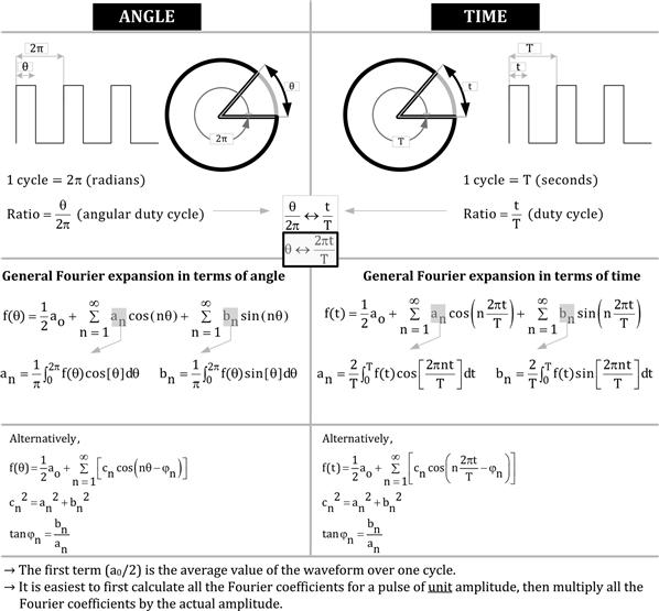
Figure 18.1: Applying Fourier series in power supplies.
Note that angle θ itself may be rather confusingly called “x” or “2α” in textbooks, but nevertheless, we recognize it is an angle (in radians).
The Rectangular Wave
We use the above-mentioned mapping procedure to analyze a rectangular waveform of amplitude “A” in terms of its Fourier series. Assume we are, for example, talking about the rectangular voltage “Vds” (same as “VDS”) across the switching FET. The results are shown in Figure 18.2. We have first analyzed the wave by assuming it is “ideal,” that is, with zero crossover (switch transition) time. We then get the following Fourier coefficients (with 2πt/T replacing θ, and pulse width designated as tON):
![]()
where ![]() and |cn| represents the magnitude of the amplitudes of the nth harmonic. We are interested in magnitudes because a conducted EMI scan doesn’t care about the signs. However, we do need the signs to correctly reconstruct the original waveform. In general, we can sum only a few terms of the Fourier series to get fairly close to the original waveform. Summed up to “nmax” harmonics, we get Vds (as a function of time)
and |cn| represents the magnitude of the amplitudes of the nth harmonic. We are interested in magnitudes because a conducted EMI scan doesn’t care about the signs. However, we do need the signs to correctly reconstruct the original waveform. In general, we can sum only a few terms of the Fourier series to get fairly close to the original waveform. Summed up to “nmax” harmonics, we get Vds (as a function of time)
![]()
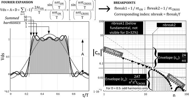
Figure 18.2: Fourier series in power supplies and plotting the Fourier coefficients.
Note that the first term is AD (amplitude times duty cycle), is just the average (DC) value of the waveform over the full time period T. We should remember that the average value is always the first term (the “n=0” term) in any Fourier expansions, and also that it is in fact irrelevant to EMI calculations since the CISPR-22 range starts at 150 kHz. However, besides the signs, the DC term is also required to correctly reconstruct the original waveform, as we have done in Figure 18.2 with a unity amplitude wave of 50% duty cycle as an example. We have summed over 1, 5, 10, 50, and finally 10,000 harmonics (not shown). We see how we move from an offset sine wave (when we sum only the n=0 and n=1 terms) to a perfectly rectangular waveform (with a very large n, we get the exact waveform we started with).
However, so far we have assumed zero crossover time. If we have a real-world situation with nonzero crossover times, then, instead of a rectangular waveform, we get a trapezoid. The Fourier coefficients get modified by an additional term below
![]()
We now have a product of two functions of the type sin(x)/x, instead of one. We need to understand what the properties of this function are.
The Sinc Function
The function sin(γ)/γ is called the sinc function. Its key properties are shown in Figure 18.3. On a log versus log plot (lowermost plot), it appears “flat-topped” at lower frequencies, with a unity value initially. In reality it is actually sloping rather gently downward, and at γ=1 its value is sin(1)=0.84. We call that a “breakpoint” because right after that, the slope changes dramatically. At higher frequencies it falls off with a slope of −20 dB/decade, a straight line on a log versus log plot. Note that the sinc function can be considered “clamped” to 1, for all frequencies less than the break frequency.
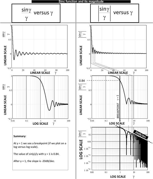
Figure 18.3: Understanding the sinc function.
When we have two breakpoints, as in the equation for the real-world cn’s above (one for tON, the other for tCROSS) we eventually see a downward slope of −40 dB/decade (obvious in the lowermost right-hand plot of Figure 18.2). Each breakpoint has clearly contributed −20 dB/decade to that slope. The actual breakpoints in terms of frequency are obtained by setting γ to 1. We thus get
![]()
In terms of the harmonic index “n” – imagining “n” varies smoothly, rather than just having integral values
![]()
Note that nbreak1 is less than 1 for duty cycles greater than 32%. Which means for all practical purposes it then becomes “invisible” since we start off with n=1.
![]()
In other words, the duty cycle needs to be below 0.32 for the first breakpoint to be “visible” (in terms of affecting any amplitudes of the Fourier terms). Otherwise, it occurs at frequencies below the fundamental frequency, and therefore can’t determine any of the actual harmonic amplitudes (i.e., n≥1). Of course, the effect of this first breakpoint is felt at almost all frequencies, since it imparts a downward slope of −20 dB/decade for all frequencies exceeding it (and likewise, clamps harmonic amplitudes below it, if any).
The Envelope of the Fourier Amplitudes
For designing the conducted EMI filters, we are not concerned with the granularity of the actual harmonic amplitudes. What matters to us is their envelope. That is what we really try to adjust and try to keep within the EMI limit lines, because even a single point in excess of the limits represents a failed EMI test. We see from Figure 18.2 (D=0.5) and from Figure 18.4 (D=0.2) that there is one breakpoint which is dependent on the switching frequency. After that breakpoint, the envelope of the amplitudes falls off as per 1/n, which is equivalent to a slope of −20 dB/decade. As per the equations in Figure 18.2, we have described the envelope as
![]()
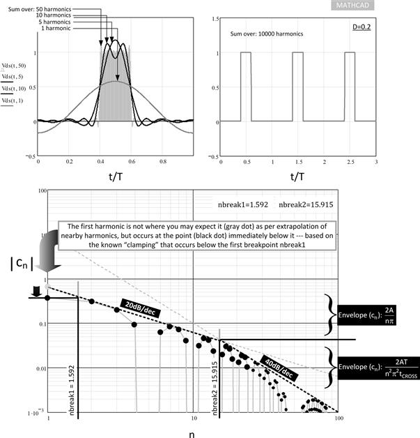
Figure 18.4: Fourier coefficients for a unity amplitude trapezoid with D=0.2.
This equation is easy to understand since we know that the actual harmonic amplitudes (for a square waveform) are
![]()
Since for all angles (and all duty cycles), the maximum value of the sine term (in the rectangle border above) is unity, the envelope must be described by “2A/nπ.” And that is the envelope equation we have provided in Figure 18.2.
However, we see that there is a second breakpoint, after which the envelope falls off as per 1/n2, which is basically equivalent to −40 dB/decade. The location of this breakpoint depends on the crossover time. We can visualize the second breakpoint as adding another −20 dB/decade to the already falling −20 dB/decade curve, leading to a cumulative slope of (−20)+(−20)=−40 dB/decade. The envelope after the second breakpoint is
![]()
Note that the original equation for cn included duty cycle, whereas the envelope equations do not (because we have “maxed out” the terms). So yes, the harmonic amplitudes do go up and down with respect to D, but the envelope remains fixed and independent of D, as we can see in Figures 18.2 and 18.4. Note that D does enter the picture if it is below 32% as we see in the example below.
Example 1
What are the amplitudes of the fundamental frequency (first harmonic), the second and the third harmonics of the VDS waveform of a 100 kHz universal input (upper limit 270VAC) AC–DC flyback converter with 5 V output and turns ratio of 19?
From Chapter 3 we know that VOR=turns ratio×VO=19×5=95 V. The duty cycle at high line (270VAC, rectified 382VDC) is D=VOR/(VIN+VOR)=0.2. In Figure 18.4, we have plotted out the results of the Mathcad file originally used for Figure 18.2, but this time performed for D=0.2. Note that we have assumed unit amplitude in these plots, knowing that everything will scale proportionally to the amplitude.
Note that if the converter is operating in “continuous conduction mode” (CCM) at high line (unlikely) we can assume a simple rectangular VDS waveform. That assumption will give accurate results for conducted mode EMI calculations even if the converter is in DCM.
The height (amplitude) of the rectangular VDS (same as Vds in this chapter) pulse is VIN+VOR=382+95=477 V (ignoring the leakage inductance spike). From Figure 18.2 we know that the magnitude of the harmonic Fourier coefficients is
![]()
We thus get three harmonic amplitudes based on the exact Fourier coefficient equations above
![]()
That is what we essentially plotted in Figure 18.4 for unit amplitude. We can confirm the graph matches the results of the calculations above, by scaling the numbers “eye-balled” from the graph (i.e., 0.38, 0.3, and 0.2 for the first three harmonics, i.e., the solid black dots), for the case of A=477 V as follows:
![]()
We see the graphical-based results are close enough to the accurate calculation above.
However, now, coming to the equation for the envelope (before the second breakpoint), we get
![]()
Using this simplified equation, we get for the three harmonics
![]()
We see a close match with the terms n=2 and n=3, but not for n=1. The actual harmonic amplitude is only about 180 V based on our exact and graphical calculations above, not 304 V. In other words, the envelope equation is now giving misleading results for the first (fundamental) harmonic. To avoid overdesign of the filter we should understand the reason for this carefully. It is explained in Figure 18.4 too. The basic reason is that since the duty cycle was lower than 32%, the first breakpoint is “visible” at an effective n of 1.592, and it therefore clamps the amplitude of the n=1 term. In Figure 18.4, as per the envelope equation, we would have got the solid gray dot as the first harmonic amplitude (roughly between 0.6 and 0.7). In reality, we get the solid black dot (a little below 0.4).
However, we can actually rather cleverly, use the envelope equation itself to predict the amplitude of the first harmonic. This is shown as follows. The equivalent “breakpoint index” is
![]()
Note that in effect we are now implicitly assuming that “n” can be a continuum of values, not just a range of integers. It helps us in the math that follows, but keep in mind it has no physical significance in terms of the Fourier series. At this point, the coordinate of the envelope is
![]()
For unit amplitude, the amplitude needs to be 190.7/477=0.4. That is close enough to the actual calculation (we had gotten 0.374 for unit amplitude based on the graph in Figure 18.4 for the first harmonic). Our conclusion is just from the two equations below, we can estimate the amplitude of the first harmonic quite accurately. To re-emphasize: it is important to know the amplitude of the first harmonic most accurately, since our conducted EMI filter design is usually based on it. Here is a summary of what we need to do to quickly and generally (for any D) estimate, based on simple envelope calculations.
Practical DM Filter Design
The trapezoid we have looked at so far is a voltage waveform. But it can equally well be a current waveform if we use the “flat-top approximation” (for large inductance). In DM filter design as applied to a Buck or a Buck-Boost (or their AC–DC equivalents, the Forward converter and the flyback converter), the input current switch current is of the shape we had previously indicated in Figure 16.2. So, the DM noise source is
![]()
where ISW here refers to the center of ramp. The Boost is not considered here as its DM filter design is almost trivial, since in effect, it has a natural LC filter on its input. In Table 18.1, we have provided the height of the switch current trapezoid for all the relevant topologies (with the flat-top approximation).
Table 18.1. Switch Currents (Center of Ramp) for the Relevant Topologies.
| Topology | ISW (Switch Current) |
| Buck | IO |
| Forward | IO×(NS/NP) |
| Buck-Boost | IO/(1−D) |
| Flyback | IO×(NS/NP)/(1−D) |
If there was no EMI filter present, the switching noise current received by the LISN would be
![]()
(since the LISN has an impedance of 100 Ω for DM noise).
However, the analyzer itself only measures the noise across one of the two effective series 50 Ω resistors in the LISN. So, the measured level of noise is
![]()
We have assumed that CBULK is very large, and that it has no ESL, and also that its ESR is much less than 100 Ω. All reasonable assumptions of course.
Note that to be more accurate and avoid overdesign, we need to split ISW into harmonic components as in the following example.
Example 2
What is the DM noise spectrum at 270VAC as measured at the LISN, for a 100 kHz universal input flyback with output of 5 V at 15.2 A? The transformer turns ratio is 19. Assume 200 ns rise and fall times. We are using an aluminum electrolytic bulk capacitor whose datasheet states that it has a capacitance of 270 μF, a dissipation factor (tangent of loss angle) of tan δ=0.15 as measured at 120 Hz, and a frequency multiplier factor of 1.5 at high frequencies.
See Figure 18.5 for this entire example. Also read the section in Chapter 16, titled “The Road to Cost-Effective Filter Design.”
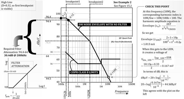
Figure 18.5: DM filter calculation for universal input flyback (see solved example).
ESR Estimate
The ESR is to be first computed at the 120 Hz test frequency. By definition
![]()
At a high frequency, the ripple current is allowed to increase by the frequency multiplier of 1.5. If the ESR had not changed, the heating, that is, I2R would have gone up by the factor 1.5×1.5=2.25. Clearly, the dissipation has remained the same (which is the reason for allowing the current to increase). This implies that the ESR falls by the factor 1/2.25=0.44 at high frequencies. Therefore, for our purpose, the high-frequency ESR value to use is
![]()
DM Calculations at High Line
See Figure 18.5 for this entire calculation.
(a) Duty Cycle and Current Trapezoid
The maximum peak rectified voltage is 270×1.414=382 V. The VOR is by definition 5 V×19=95 V. The lowest duty cycle (highest input) is
![]()
Load current of 15.2 A translates to the following switch current pedestal based on Table 18.1.
![]()
(b) Breakpoints
As in Example 1, we see that the index and corresponding frequency breakpoints are
![]()
![]()
![]()
![]()
We see that fbreak1 exceeds the fundamental frequency of 100 kHz, so its amplitude will get clamped. We use the envelope equations previously provided, to find out the exact amplitude of the first harmonic. It is
![]()
The second Fourier harmonic (based on envelope) is at 200 kHz and of amplitude
![]()
(c) EMI Spectrum with no Filter
Above, we have calculated the harmonic current amplitudes based on an envelope estimate. When these current harmonics reach the LISN, still assuming no EMI filter, we get the following voltages:
![]()
![]()
(d) Required Filter Attenuation
From the equation in Figure 15.3, over the range 150–500 kHz, the equation for the quasi-peak limit of CISPR-22 Class B is
![]()
At the second harmonic of the no-filter spectrum (200 kHz), this limit is
![]()
So, looking at Figure 18.5, we get the required filter attenuation as 94.4−64=30.4 dB at 200 kHz. We are ignoring the fundamental since it lies outside the CISPR range.
(e) Calculating Filter Components at Stated Line Condition
We therefore need to pick a low-pass LC filter with an appropriate corner frequency (“pole” in Figure 18.5) that provides this attenuation. For example, if we are using a one-stage LC low-pass filter, we know it has an attenuation characteristic of about 40 dB/decade above its corner frequency (i.e., ![]() ). So, the equation of the required response is (where “att” stands for “with attenuation”)
). So, the equation of the required response is (where “att” stands for “with attenuation”)
![]()
![]()
![]()
We therefore need a filter that has an LC of
![]()
For example, if we have picked the X-cap C3 in Figure 16.1 as 0.22 μF, the net DM inductance is L (twice the individual DM inductances in each line). We get
![]()
Before we build this filter, we need to repeat all the above steps at low line too (90VAC). We get another inductance recommendation as seen below.
DM Calculations at Low Line
(a) Duty Cycle and Current Trapezoid
![]()
![]()
![]()
![]()
![]()
![]()
We see that fbreak1 is below the fundamental frequency of 100 kHz. So, it will not affect any harmonic amplitudes. The amplitude of the first harmonic (at 100 kHz) is then just based on the simple equation below.
![]()
The second Fourier harmonic (based on envelope) is at 200 kHz and of amplitude
![]()
(c) EMI Spectrum with no Filter
![]()
![]()
(d) Required Filter Attenuation
At the second harmonic of the no-filter spectrum (200 kHz), the CISPR Class B limit is
![]()
So, the required filter attenuation is 96.8−64=32.8 dB at 200 kHz.
(e) Calculating Filter Components at Stated Line Condition
![]()
We therefore need a filter that has an LC of
![]()
For example, if we have picked the X-cap C3 in Figure 16.1 as 0.22 μF, the net DM inductance required is L (twice the individual DM inductances in each line). We get
![]()
At high line we had 48 μH, at low line we get 63 μH on account of the higher currents at low line. Our final choice is the greater of the two, that is, 63 μH.
The chosen inductor must not saturate on account of the very high peak AC currents, and we should evaluate that once again, both at low line and at high line. To find the worst-case peak AC current in the filter, we need to look at the equations in Chapter 14. That helps us in picking the right size of DM inductor. We also need to ensure the quality factor of the inductor is lower than unity, to avoid ringing. For that we need to ensure enough DCR. If that makes it too lossy, we can consider raising the Q to 1.5 or 2, provided we have some additional headroom in the EMI scan.
Filter Safety Margin
We will need to include some safety margin that we have not included above. Typically, a margin of about 10–12 dB may be necessary. So far we have assumed no CM noise, whereas the CISPR limit lines constitute a mix of both CM and DM noise. Therefore, if we want to leave margin for that, and make the simplest assumption that the CM and DM noise contributions are equal, we then need to lower the DM noise level to half of what we have so far allowed above. Further, since 20×log(2)=6 dB, this implies we need to leave a DM margin of 6 dB just for possible CM noise encroaching on our measurements. In addition, the certification lab or OEM may want us to demonstrate say, 3 dB margin, to ensure compliance over production lots. So, in all we should plan for a margin of 10 dB. We may therefore go back to “step d” and set the required attenuation to 30.4+10=40.4 dB instead. Then all the steps are the same.
Note: We can ask — since the breakpoint associated with the rise and fall times didn’t enter the picture here, does that mean that it doesn’t matter how fast we turn-on and turn-off the FET? Yes, from the DM noise viewpoint it really doesn’t matter (much). However, there are parasitics that we have ignored (chiefly the ESL and trace inductances). And since, unlike the ESR, these will produce frequency-dependent voltage spikes, it is in our interest not to keep the FET crossover (transition) times too small.
Note: If our switching frequency was greater than 150k, then the first harmonic at low line, which is very high indeed (being unclamped by the first breakpoint), would have appeared in the CISPR range. That would have made the DM filter much bigger.
Practical CM Filter Design
Having understood that the worst-case for DM filter design is at low line, on account of the higher currents, we can sense that the worst-case common mode noise will occur at high line since the voltages are highest; and as described in Figure 16.5 that will lead to the highest injected currents into the enclosure. Let us therefore do this calculation at high line only. Let us also ignore the second breakpoint as we have already seen it is too far away to affect the filter design per se. Note that we are assuming that by using the X-cap C1 in Figure 16.3, this truly is CM noise, not mixed mode (MM) noise.
Example 3
This is a continuation of Example 2. What is the corresponding CM noise spectrum assuming a mounting capacitance of 100 pF (to earth)?
CM Calculations at High Line
See Figure 18.6 for this entire example.
(a) Duty Cycle and Current Trapezoid
The maximum peak rectified voltage is 270×1.414=382 V. The VOR is by definition 5 V×19=95 V. The lowest duty cycle (highest input) is
![]()
The VDS amplitude for a flyback is VIN+VOR=382+95=477 V. If this were a single-ended Forward converter, we could use 2×VIN=764 V. This is “A” (pulse amplitude) in the Fourier expansion.
(b) Breakpoints
As in Example 1, we see that the index and corresponding frequency breakpoints are as follows:
![]()
![]()
![]()
The second Fourier harmonic (based on envelope) is at 200 kHz and of amplitude
![]()
(c) EMI Spectrum with no Filter
Above, we have calculated the harmonic voltage amplitudes based on an envelope estimate. These generate harmonic currents in the line, based on the impedance in the path including the LISN.
![]()
Similarly for the second harmonic (frequency fSW),
![]()
Using the fact that the magnitude of an imaginary number c/(a−jb) equals c/(a2+b2)0.5, we get the following magnitudes of harmonic currents


Note the rather astonishing result: the amplitudes of the different harmonic CM currents are the same — there is no 20 dB/decade roll-off anymore.
These harmonic currents flow through the 25 Ω equivalent CM LISN impedance and get converted into voltage picked up by the spectrum analyzer as per Vcm=25×Icm. So we get
![]()
Note that in Chapter 16 we had stated that
![]()
Let us check if this is borne out. We get
![]()
Summary: The CM noise spectrum is flat-topped (clamped) at exactly 100×A×CP/T, right up till the second breakpoint (not discussed above). We know that all the harmonic amplitudes fall off by (an additional) 20 dB/decade after fbreak2=1/πtCROSS, and therefore, so does Vcm_n (as per the property of the sinc function). We thus conclude our analysis with the CM envelope plot shown in Figure 18.6.
(d) Required Filter Attenuation
At 50 kHz, the CISPR Class B (QP) limit is 66 dB μV.
So, looking at Figure 18.6, we get the required filter attenuation as 47.6 dB at 150 kHz.
Note: As explained in Chapter 16 under “The Road to Cost-effective Filter Design,” even though the CM noise spectrum is flat, since the pole of the LC filter is always well below 150 kHz, the CM noise spectrum after inserting the filter will fall at −40 dB/decade. Since the CISPR-22 Class B limit is falling at −20 dB/decade, the CM noise spectrum will accrue an “advantage” of 20 dB/decade as the frequency rises. So, if we ensure that we are compliant at the lowest frequency (150 kHz), we are assured (theoretically) that we will be automatically compliant at higher frequencies.
(e) Calculating Filter Components at Stated Line Condition
We therefore need to pick a low-pass LC filter with an appropriate corner frequency (“pole” in Figure 18.6) that provides this attenuation. For example, if we are using a one-stage LC low-pass filter, we know it has an attenuation characteristic of about 40 dB/decade above its corner frequency (i.e., 1/2π√(LC)). So, the equation of the required response is
![]()
We therefore need a filter that has an LC of
![]()
For example, suppose we have finally picked two Y-caps marked “C4” in Figure 16.1 as 2.2 nF each (no “C2” caps are present in view of the safety restrictions on total Y-capacitance as also discussed in Chapter 16). Then, as per the equivalent diagram, the effective C is therefore 4.4 nF. We can thus find Lcm as follows.
![]()
This is a very high inductance. We may therefore consider two identical CM filters (LC stages) in cascade instead. Let us also split the Y-cap into four 1.2 nF caps, so each stage gets a total Y-capacitance of 2.4 nF. That way we will not exceed the safety requirements.
Now, two LC filters in cascade will give us 80 dB/decade attenuation. Therefore, we get
![]()
![]()
![]()
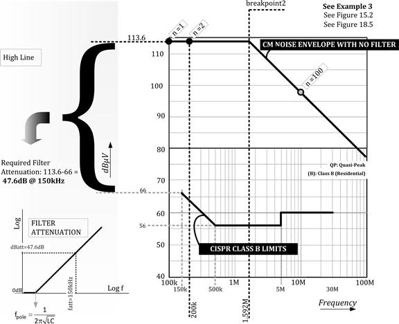
Figure 18.6: CM filter calculation for universal input flyback (see solved example).
This is a readily available value, with an inductance about 10 times smaller than our first calculation with only one CM stage. Though we have two CM stages instead of one, the net savings in terms of total volume occupied by the CM chokes is about 10/2=5 times. Our conclusion is we really need a two-stage CM filter to comply with CISPR-22 Class B conducted EMI requirements. Note that the “accidental” CM stage in Figure 16.1 consisting of Lcm/2 and C3 usually has a pole at a much higher frequency, so it will not be able to do much here. We should plan on a full extra CM stage.