DSP Architectures
General-purpose processors are designed to have broad functionality. These processors are designed to be used in a wide variety of applications. The performance goal of general-purpose processors is maximized performance over a broad range of applications. Specialized processors, on the other hand, are designed to take advantage of the limited functionality required by their applications to meet specific objectives. DSPs are a type of specialized processor. These processors are designed to focus on signal processing applications. Hence, there is little or no support to date for features such as virtual memory management, memory protection, and certain types of exceptions.
DSPs, as a type of specialized processor, have customized architectures to achieve high performance in signal processing applications. Traditionally, DSPs are designed to maximize performance for inner loops containing a product of sums. Thus, DSPs usually include hardware support for fast arithmetic, including single cycle multiply instructions (often both fixed-point and floating-point), large (extra wide) accumulators, and hardware support for highly pipelined, parallel computation and data movement. Support for parallel computation may include multiple pipelined execution units. To keep a steady flow of operands available, DSP systems usually rely on specialized, high bandwidth memory subsystems. Finally, DSPs feature specialized instructions and hardware for low overhead loop control and other specialized instructions and addressing modes that reduce the number of instructions necessary to describe the typical DSP algorithm.
Fast, Specialized Arithmetic
DSPs were designed to process certain mathematical operations very quickly. A seven tap FIR filter processing a 400 KHz signal, for example, must complete over 5.6 million multiplies and 5.6 million adds per second. DSP vendors recognized this bottleneck and have added specialized hardware to compute a multiply in only one cycle. This dramatically improves the throughput for these types of algorithms.
Another distinguishing feature of a DSP is its large accumulator register or registers. The accumulator is used to hold the summation of several multiplication operations without overflowing. The accumulator is several bits wider than a normal processor register which can help avoid overflow during the accumulation of many intermediate results. The extra bits are called guard bits. In DSPs the multiplier, adder and accumulator are almost always cascaded so that the “multiply and accumulate” operation so common to DSP algorithms can be specified in a single specialized instruction. This instruction (typically called a MAC) is one example of how DSPs are optimized to reduce the number of instruction fetches necessary for DSP algorithms. I’ll describe others later in this chapter.
The MAC unit
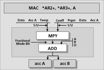
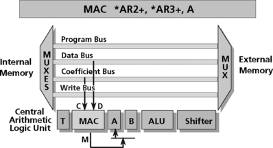
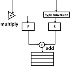
At the core of the DSP CPU is the “MAC” unit (for multiply and accumulate), which gets its name from the fact that the unit consists of a multiplier that feeds an accumulator. To feed the multiplier most efficiently, a “data” bus is used for the “x” array, and a “coefficient” bus is used for the “a” array. This simultaneous use of two data buses is a fundamental characteristic of a DSP system. If the coefficients were constants, the user might want to store them in ROM. This is a common place to hold the program, and it allows the user to perform the MAC operations using coefficients stored in program memory and accessed via the program bus. Results of the MAC operation are built up in either of two accumulator registers. Both of these registers can be used equally. This allows the program to maintain two chains of calculations instead of one. The MAC unit is invoked with the MAC instruction. An example of a MAC instruction is shown in Figure 5.1. This one instruction is performing many operations in a single cycle; it reads two operands from memory, increments two pointers, multiplies the two operands together, and accumulates this product with the running total.
Parallel ALUs
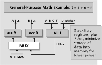
Most DSP systems need to perform lots of general-purpose arithmetic (simple processes of addition and subtraction). For this type of process, a separate arithmetic logic unit (ALU) is often added to a DSP. The results of the ALU can be basic math or Boolean functions. These results are sent to either of the accumulators seen before. The ALU performs standard bit manipulation and binary operations. The ALU also has an adder. The adder assures efficient implementation of simple math operations without interfering with the specialized MAC unit.
Inputs to the ALU are, as with the MAC unit, very broad to allow the user maximum flexibility in obtaining efficient code implementation. The ALU can use either accumulator and the data and/or coefficient buses as single or dual inputs (Figure 5.2). The ALU generates the standard status bits including overflow flags for both A and B, zero flags for both A and B, and a carry bit for both A and B.
Numeric representation
While DSP units have traditionally favored fixed-point arithmetic, modern processors increasingly offer both fixed- and floating-point arithmetic. Floating-point numbers have many advantages for DSPs;
First, floating-point arithmetic simplifies programming by making it easier to use high level languages instead of assembly. With fixed-point devices, the programmer must keep track of where the implied binary point is. The programmer must also worry about performing the proper scaling throughout the computations to ensure the required accuracy. This becomes very error-prone and hard to debug as well as to integrate.
Floating-point numbers also offer greater dynamic range and precision than fixed-point. Dynamic range is the range of numbers that can be represented before an overflow or an underflow occurs. This range effectively indicates when a signal needs to be scaled. Scaling operations are expensive in terms of processor clocks and so scaling affects the performance of the application. Scaling data also causes errors due to truncation of data and rounding errors (also known as quantization errors). The dynamic range of a processor is determined by size of the exponent. So for an 8-bit exponent the range of magnitudes that can be represented would be:
Floating-point numbers also offer greater precision. Precision measures the number of bits used to represent numbers. Precision can be used to estimate the impact of errors due to integer truncation and rounding. The precision of a floating-point number is determined by the mantissa. For a 32 bit floating-point DSP, the mantissa is generally 24 bits. So the precision offered by a 32 bit DSP with a mantissa of 24 bits is at least that of a 24 bit fixed-point device. The big difference is that the floating-point hardware automatically normalizes and scales the resultant data, maintaining 24 bit precision for all numbers large and small. In a fixed-point DSP, the programmer is responsible for performing this normalization and scaling operation.
Keep in mind that floating-point devices have some disadvantages as well:
• Algorithmic issues – Some algorithms, such as data compression, do not need floating-point precision and are better implemented on a fixed-point device.
• More power – Floating-point devices need more hardware to perform the floating-point operations and automatic normalization and scaling. This requires more die space for the DSP, which takes more power to operate.
• Slower speed – Because of the larger device size and more complex operations, the device runs slower than a comparable fixed-point device.
• More expensive – Because of the added complexity, a floating-point DSP is more expensive than fixed-point. A trade-off should be made regarding device cost and software programmer cost when programming these devices.
High Bandwidth Memory Architectures
There are several ways to increase memory bandwidth and provide faster access to data and instructions. The DSP architecture can be designed with independent memories allowing multiple operands to be fetched during the same cycle (a modified Harvard architecture). The number of I/O ports can be increased. This provides more overall bandwidth for data coming into the device and data leaving the device. A DMA controller can be used to transfer the data in and out of the processor, increasing the overall data bandwidth of the system. Access time to the memory can be decreased, allowing data to be accessed more quickly from memory. This usually requires adding more registers or on-chip memory (this will be discussed more later). Finally, independent memory banks can be used to reduce the memory access time. In many DSP devices, access time to memory is a fraction of the instruction cycle time (usually ½, meaning that two memory accesses can be performed in a single cycle). Access time, of course, is also a function of memory size and RAM technology.
Data and Instruction Memories
DSP-related devices require a more sophisticated memory architecture. The main reason is the memory bandwidth requirement for many DSP applications. It becomes imperative in these applications to keep the processor core fed with data. A single memory interface is not good enough. For the case of a simple FIR filter, each filter tap requires up to four memory accesses:
• Read the corresponding coefficient value.
• Write the sample value to the next memory location (shift the data).
If this is implemented using a DSP MAC instruction, four accesses to memory are required for each instruction. Using a von Neumann architecture, these four accesses must all cross the same processor/memory interface, which can slow down the processor core to the point of causing it to wait for data. In this case, the processor is “starved” for data and performance suffers.
In order to overcome this performance bottleneck, DSP devices often use several buses to interface the CPU to memory: a data bus, a coefficient bus, and a program bus (Figure 5.3). All of these move data from memory to the DSP. An additional bus may be available to store results back out to memory. During each cycle, any number of buses may access the arrays of internal memory, and any one bus may talk to an external device. Internal control logic in a DSP prevents the possibility of bus collision if several buses try to access off-chip resources at the same time.
In order for the MAC instruction to execute efficiently, multiple buses are necessary to keep data moving to the CPU. The use of multiple buses makes the device faster1.
Memory Options
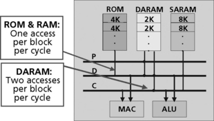
There are two different types of memories available on DSP architectures: ROM and RAM. Different DSP families and versions have different amounts of memory. Current DSPs contain up to 48K of ROM and up to 200K of RAM, depending on the specific device.
RAM comes in two forms: single access (SARAM) and dual access (DARAM). For optimum performance, data should be stored in dual access memory and programs should be stored in SARAM (Figure 5.4). The main value of DARAM is that storing a result back to memory will not block a subsequent read from the same block of memory.
High Speed Registers
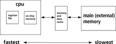
Many DSP processors include a bank of internal memory with fast, single cycle access times. This memory is used for storing temporary values for algorithms such as the FIR filter. The single cycle access time allows for the multiply and accumulate to complete in one cycle. In fact, a DSP system contains several levels of memory as shown in Figure 5.5. The register file residing on-chip is used for storing important program information and some of the most important variables for the application. For example, the delay operation required for FIR filtering implies information must be kept around for later use. It is inefficient to store these values in external memory because a penalty is incurred for each read or write from external memory. Therefore, these delay values are stored in the DSP registers or in the internal banks of memory for later recall by the application without incurring the wait time to access the data from external memory. The on-chip bank of memory can also be used for program and/or data and also has fast access time. External memory is the slowest to access, requiring several wait states from the DSP before the data arrives for processing. External memory is used to hold the results of processing.
Memory Interleaving
DSP devices incorporate memory composed of separate banks with latches for separate addresses to these banks (Figure 5.6). The banks are interleaved sequentially. This allows multiple words to be fetched simultaneously as long as they are from a block whose length is equal to the number of banks. Bank organization can also be used to match bus bandwidths with memory access times. If separate addresses are provided, multiple words can be fetched as long as they are in different banks, a significant performance improvement in DSP applications.
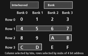
Interleaved bank organization is a special case of bank organization where all banks are addressed simultaneously and row aligned. This allows multiple accesses as long as they are from sequential addresses. This approach reduces the number of address latches required on the device.
Bank Switching
Modern DSPs also provide the capability for memory bank switching. Bank switching allows switching between external memory banks for devices requiring extra cycles to turn off after a read is performed. Using this capability, one external bus cycle can be automatically inserted when crossing memory bank boundaries inside program or data space. The DSP can also add one wait state between program and data accesses or add one wait state when crossing between user defined physical memory boundaries.
Caches for DSPs
Cache systems often improve the average performance of a system, but not the worst case performance2. This results in less value for DSP systems which depend on predictable worst case performance. Some DSPs, however, contain cache systems. These are typically smaller and simpler than general-purpose microprocessor caches. They are often used to free memory bandwidth rather than reduce overall memory latency. These caches are typically instruction (program) caches.
DSPs that do not support data caches (or self-modifying code) have simple hardware because writes to cache (and consequently coherency) are not needed. DSP caches are often software controlled rather than hardware controlled. For example, internal on-chip memory in a DSP is often used as a software controlled data cache to reduce main memory latency. On-chip memory, however, is not classified as a cache because it has addresses in the memory map and no tag support. But on-chip memory may be used as a software cache.
Repeat buffers
DSPs often implement what is called a repeat buffer. A repeat buffer is effectively a one word instruction cache. This cache is used explicitly with a special “repeat” instruction in DSPs. The “repeat” instruction will repeat the execution of the next instruction “n”
times, where n can be an immediate value or a registered integer. This is a popular and powerful instruction to use on one-instruction inner loops3.
As advanced form of the repeat buffer is the “Repeat buffer with multiple entries.” This is the same as the repeat buffer but with multiple instructions stored in a buffer. To use this instruction, the programmer must specify the block of instructions to be stored in the buffer. The instructions are copied into buffer on the first execution of the block. Once the instructions are in the block, all future passes through the loop execute out of the buffer4.
Single-entry instruction cache
A similar form of instruction cache is called a single entry instruction cache. In this configuration, only a single block of contiguous code can be in the cache at once. This type of cache system allows multiple entry points into the sequential code rather than one single entry at the beginning. This type of cache permits indirection such as jumps, gotos, and returns, to access the buffer5.
Associative instruction cache
An associative instruction cache allows multiple entries or blocks of code to reside in the cache. This is a fully associative system which avoids block alignment issues. Hardware controls which blocks are in cache. Systems of this kind often have special instructions for enabling, locking, and loading. A “manual” control capability also exists. This mode can be used to improve performance or ensure predictable response6.
Dual cache
Finally, a dual cache memory system is one that allows on-chip memory to be configured as RAM (in the memory map) or cache. The programmer is allowed to configure the mode. The advantage of this approach is that it allows an initial program to be brought up quickly using the cache and then optimized for performance/predictability if needed.
Execution Time Predictability
Specialized processors with hard time constraints, such as DSPs, require designs to meet worst case scenarios. Predictability is very important so time responses can be calculated and predicted accurately7. Many modern general-purpose processors have complex architectures that make execution time predictability difficult (for example, superscalar architectures dynamically select instructions for parallel execution). There is little advantage in improving the average performance of a DSP processor if the improvement means that you can no longer predict the worst case performance. Thus, DSP processors have relatively straightforward architectures and are supported by development and analysis tools that help the programmer determine execution time accurately.
Most DSPs’ memory systems limit the use of cache because conventional cache can only offer a probabilistic execution model. If the instructions the processor executes reside in the cache, they will execute at cache speeds. If the instruction and data are not in the cache, the processor must wait while the code and data are loaded into the caches.
The unpredictability of cache hits isn’t the only problem associated with advanced architectures. Branch prediction can also cause potential execution time predictability problems. Modern CPUs have deep pipelines that are used to exploit the parallelism in the instruction stream. This has historically been one of the most effective ways for improving performance of general-purpose processors as well as DSPs.
Branch instructions can cause problems with pipelined machines. A branch instruction is the implementation of an if-then-else construct. If a condition is true then jump to some other location; if false then continue with the next instruction. This conditional forces a break in the flow of instructions through the pipeline and introduces irregularities instead of the natural, steady progression. The processor does not know which instruction comes next until it has finished executing the branch instruction. This behavior can force the processor to stall while the target jump location is resolved. The deeper the execution pipeline of the processor, the longer the processor will have to wait until it knows which instruction to feed into the pipeline next. This is one of the largest limiting factors in microprocessor instruction execution throughput and execution time predictability. These effects are referred to as branch effects. These branch effects are probably the single biggest performance inhibitor of modern processors.
Dynamic instruction scheduling can also lead to execution time predictability problems. Dynamic instruction scheduling means that the processor dynamically selects sequential instructions for parallel execution, depending on the available execution units and on dependencies between instructions. Instructions may be issued out of order when dependencies allow for it. Superscalar processor architectures use dynamic instruction scheduling. Many DSPs on the market today (although not all) are not supserscalar for this reason—the need to have high execution predictability.
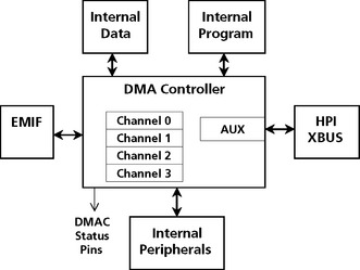
Direct Memory Access (DMA)
Direct memory access is a capability provided by DSP computer bus architectures that allows data to be sent directly from an attached device (such as a disk drive or external memory) to other memory locations in the DSP address space. The DSP is freed from involvement with the data transfer, thus speeding up overall computer operation.
DMA devices are partially dependent coprocessors which offload data transfers from the main CPU. DMA offers a high performance capability to DSPs. Modern DSP DMA controllers such as the TMS320C6x can transfer data at up to 800 Mbytes/sec (sustained). This DMA controller can read and write one 32-bit word every cycle. Offloading the work of transferring data allows the CPU to focus on computation. Typical types of transfers that a DMA may control are:
• Memory to memory transfers (internal to external).
• Transfers from I/O devices to memory.
• Transfers from memory to I/O devices.
DMA setup
Setup of a DMA operation requires the CPU to write to several DMA registers. Setup information includes information such as the starting address of the data to be transferred, the number of words to be transferred, transfer type and the addressing mode to be used, the direction of the transfers, and the destination address or peripheral for the data. The CPU signals to the DMA controller when the transaction request is complete.
The actual transfer of data involves the following steps:
1. The DMA requests the bus when it is ready to start the transfer.
2. The CPU completes any memory transactions currently in operation and grants the bus to the DMA controller.
3. The DMA transfers words until the transfer is complete or the CPU requests bus.
4. If the DMA grants the bus back before the transfer is complete, it must request it again to finish the transaction.
5. When the entire block is transferred, the DMA may optionally notify the CPU via an interrupt.
Managing conflicts and multiple requests
DMA controllers have built in features to reduce bus or resource conflict. Many DMA controllers synchronize transfers to the source or destination via interrupts. DMA controllers allow the programmer to move data off chip to on chip, or back and forth in off-chip and on-chip memory. Modern DSPs provide multiple memories and ports for DMA use. DSPs implement independent data and address buses to avoid bus conflicts with the CPU. The Texas Instruments TMS320Cx, the Motorola DSP96002, and the Analog Devices ADSP-2106x families all implement some form of DMA capability.
Multiple channel DMA capability allows the DSP to manage multiple transaction requests at once with arbitration decisions for sub block transfers based on priority as well as destination and source availability (Figure 5.9). DSP vendors refer to this capability as multiple channels but in reality this is a transaction abstraction and not a physical hardware path. Each DMA channel has its own control registers to hold the transaction’s information. The Texas Instruments TMS320C5x DSP, for example, has a six DMA channel capability (Figure 5.8).
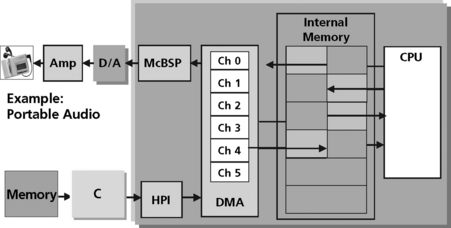
Figure 5.8 Six DMA channel capability in the Texas Instruments TMS320C5x DSP (courtesy of Texas Instruments)
The DMA available on some DSPs allows parallel and/or serial data streams to be up and/or down loaded to or from internal and/or external memory. This allows the CPU to focus on processing tasks instead of data movement overhead.
DMA Example
In the portable audio example of Figure 5.8, the DMA synchronizes the retrieval of compressed data from the mass storage as well as the flow of uncompressed data through the DAC into the stereo headphones. This frees the CPU to spend 100% of its cycles on what it does best—performing DSP functions efficiently.
DSP-specific features
DMA controllers are not just good at efficient data transfer. They often provide useful data manipulation functions as well, such as sorts and fills. Some of the more complex modes include:
• Circular addressing – This mode is very useful when the application is managing a circular buffer of some type.
• Bit reversal – This mode is efficient when moving the results of a FFT, which outputs data in bit-reversed order.
• Dimensional transfers such as 1D to 2D – This mode is very useful for processing multidimensional FFT and filters.
• Striding though arrays – This mode is useful when the application, for example, needs to access only the DC component of several arrays of data.
Host Ports
Some DSP memory systems can also be accessed through a “host port.” Host port interfaces (HPIs) provide for connection to a general-purpose processor. These host ports are specialized 8 or 16 bit bidirectional parallel ports. This type of port allows the host to perform data transfers to DSP memory space. Some host interfaces allow the processor to force instruction execution or interrupt setting on architectural state probing. Host ports can be used to configure a DSP as a partially dependent coprocessor. Host ports are also often used in development environments where users work on the host, which controls the DSP.
In general, the HPI is an asynchronous 8 or 16 bit link (depending on the device), intended for facilitating communication across a glueless interface to a wide array of external ‘host’ processors. Numerous control pins are available to allow this variety of connection modes and eliminate the need to clock the host with the DSP. The host port allows a DSP to look like a FIFO-like device to the host, greatly simplifying and cost reducing the effort of connecting two dissimilar processors. The HPI is very handy for booting a ROM-less DSP from a system host, or for exchanging input data and results between a DSP and host at run-time (Figure 5.10).
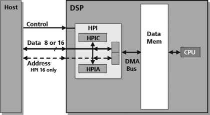
Figure 5.10 The host port interface can be used to transfer large amounts of data to and from a host (courtesy of Texas Instruments)
In the solid-state portable audio application of Figure 5.11, the DMA reads the flash card memory using the EMIF (one of the memory options). The extended address reach allows the DMA to access the entire memory space of a flash card8. This is shown in abstract form in Figure 5.11. The 16 bit connection in Figure 5.10 is a data connection which transfers the 16 bit words to and from memory. The 23 bit connection is the address bus (8 MWords range). Different DSP devices have different extended program address reach (these devices may also have 16 bit I/O and data spaces, 64KWords apiece).
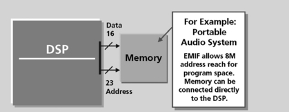
Figure 5.11 External memory interface provides flexibility for off-chip memory accesses (courtesy of Texas Instruments)
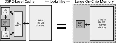
For off-chip memory accesses, the EMIF bus is active. This consumes power. By using internal memory, power consumption is reduced. Since the external buses are not used, the clock to these external buses can be stopped, which saves power. Since the internal memory operates at the core voltage of the DSP instead of the voltage of the external SRAM and EMIF buses, it consumes less power (Figure 5.12).
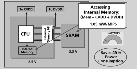
Figure 5.12 Internal memory on a DSP reduces power and increased performance (courtesy of Texas Instruments)
8CompactFlash cards are available in capacities from 4 MB to over 128 MB, SmartMedia cards are available in capacities of 2MB to over 8 MB. In this example a card no larger than 8 MB would be used.
Pipelined Processing
In DSP processors, like most other processors, the slowest process defines the speed of the system. Processor architectures have undergone a transformation in recent years. It used to be that CPU operations (multiply, accumulate, shift with incrementing pointers, and so on) dominated the overall latency of the device and drove the execution time of the application. Memory accesses were trivial. Now it’s the opposite. Geometries are so small that CPU functions can go very fast, but memory hasn’t kept up. One solution to this problem is to break the instruction execution into smaller chunks. This way, while the processor is waiting for a memory access it can be performing at least part of the work it is trying to do.
When the various stages of different instances of an operation are overlapped in time, we say the operation has been pipelined. Instruction pipelines are a fundamental element of how a DSP achieves its high order of performance and significant operating speeds.
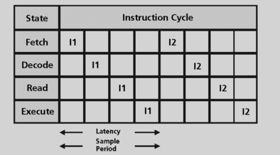
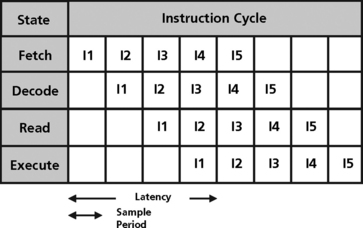
When any processor implements instructions, it must implement these standard sub-actions, or “phases” (Figure 5.13):

• Prefetch – Calculate the address of the instruction. Determine where to go for the next line of code, usually via the “PC” or program counter register found in most processors.
• Fetch – Collect the instruction. Retrieve the instruction found at the desired address in memory.
• Decode – Interpret the instruction. Determine what job it represents, and plan how to carry it out.
• Access – Collect the address of the operand. If an operand is required, determine where in data memory the value is located.
• Read – Collect the operand. Fetch desired operand from data memory.
• Execute; the instruction – or “do the job” desired in the first place.
In a DSP, each of these sub-phases can be performed quickly, allowing us to achieve the high MIP rates.
All instructions must pass through these phases to be implemented. Each sub-phase takes one cycle. This sounds like a lot of overhead when speed is important. However, since each pipeline phase uses separate hardware resources from each other phase, it is possible for several instructions to be in process every cycle (Figure 5.14).
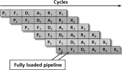
As shown in Figure 5.14, instruction 1 (P1) first implements its prefetch phase. The instruction then moves to the fetch phase. The prefetch hardware is therefore free to begin working on instruction 2 (P2) while instruction 1 is using the fetch hardware. In the next cycle, instruction 1 moves on to the decode phase (D1), allowing instruction 2 to advance to the fetch phase (F2), and opening the prefetch hardware to start on instruction 3. This process continues until instruction 1 executes. Instruction 2 will now execute one cycle later, not six. This is what allows the high MIPs rate offered in pipelined DSPs. This process is performed automatically by the DSP, and requires no awareness on the part of the programmer.
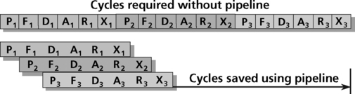
Figure 5.15 shows the speed improvements to be gained by executing multiple instruction in parallel using the pipeline concept. By reducing the number of cycles required, pipelining also reduces the overall power consumed.
Adding pipeline stages increases the computational time available per stage, allowing the DSP to run at a slower clock rate. A slower clock rate minimizes data switching. A CMOS circuit consumes power when you switch. So requirements reducing the clock rate leads to lower power requirements9. The trade-off is that large pipelines consume more silicon area. In summary, pipelining, if managed effectively, can improve the overall power efficiency of the DSP.
Atomic instructions assume a processor that operates in synch with a clock whose cycle time is Tc. The instructions are treated atomically; that is, one completes before the next one starts. An instruction consists of an integral number (N) of states (possibly 1) with a latency (L = N * Tc). Then program execution time is the sum of the latency time of each instruction in the dynamic stream executed by the processor (Figure 5.16).
One of the advantages of atomic instructions is that they reduce hardware cost to a minimum. Hardware resources can have maximum reuse within an instruction without conflicting with other instructions. For example, the ALU can be used for both address generation and data computation. State and value holding hardware can be optimized for single instruction processing without regard to partitioning for simultaneous instructions. Another advantage of atomic instructions is that they offer the simplest hardware and programming model.
Atomic execution minimizes the hardware but is not necessarily hardware efficient. Atomic execution allows reuse between stages. The ALU, for example, can perform address computation and data computation at the same time. Cycle time and latency can also be optimized to minimize the hardware with regard to pipeline partitioning. Overall, pipeline hardware is used more efficiently than nonpipeline hardware. Hardware that is associated with each stage of computation is used every cycle instead of 1/N cycles for a N stage deep pipeline.
In an ideal pipeline, all instructions go through a linear sequence of states with the same order and the same number of states (N) and latency (L = N * Tc). An instruction starts after the previous instruction leaves its initial state. Therefore, the rate of instruction starts is 1/Tc (Figure 5.17). Program execution time is the number of dynamic instructions multiplied by the cycle time plus the latency of the last instruction.
Pipeline hardware is used more efficiently in the ideal case. Hardware associated with each stage is used every cycle instead of 1/N cycles. (Some blocks within a stage may not be used).
Limitations
The depth of the pipeline is often increased to achieve higher clock rates. The less logic per stage, the smaller the clock period can be and the higher the throughput. Increasing MHz helps all instructions. There are limits to the throughput that can be gained by increasing pipeline depth, however. Given that each instruction is an atomic unit of logic, there is a loss of performance due to pipeline flushes during changes in program control flow. Another limitation to pipelines is the increased hardware and programmer complexity because of resource conflicts and data hazards. These limitations cause latency which has a significant impact on overall performance (on the order of MHz impact). Sources of latency increase, including register delays for the extra pipeline stages, register setup for the extra stages, and clock skew to the additional registers.
The factors that prevent pipelines from achieving 100% overlaps include:
• Resource Conflicts – Two or more instructions in the pipeline need the same hardware during the cycle.
• Data Hazards – A subsequent instruction needs the result of a previous instruction before it has completed.
• Branch Control Flow – Change in flow due to a branch results in not knowing how to resolve the next instruction fetch until the branch has completed.
• Interrupt Control Flow – Change in flow due to a interrupt results in the any interrupt needing to be inserted atomically.
Resource Conflicts
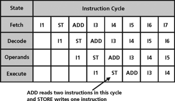
As an example of a resource conflict, assume a machine with the following scenario:
• A Fetch, Decode, Read, Execute pipeline,
• A two-port memory, both ports of which can read or write,
• An ADD *R0, *R1, R2 instruction that reads the operands in the read stage,
• A STORE R4 *R3 instruction that reads the operand during the read stage, and stores to the memory in the execute stage.
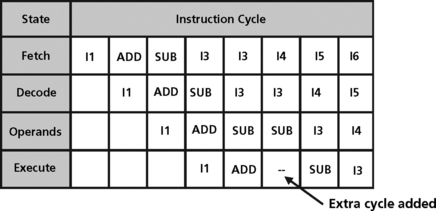
This machine can execute a sequence of adds or stores in an ideal pipeline. However, if a store precedes the add then during the cycle where add is in the read stage and the store in execute stage, the memory with two ports will be asked to read two values and store a third (Figure 5.18).
One solution to the resource conflict just described is for the programmer to insert a NOP between the store and the add instructions. This introduces a delay in the pipeline that removes the conflict, as shown in Figure 5.19. When the programmer must do this to prevent the conflict, the pipe is said to be unprotected or visible.
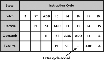
In some DSPs, the hardware detects the conflict and stalls the store instruction and all subsequent instructions for one cycle. This is said to be a protected or transparent pipeline. Regardless of whether the programmer or the hardware has to introduce the delay, the cycles per instruction performance of the CPU degrades due to the extra delay slot.
Resource conflicts are caused by various situations. Following are some examples of how resource conflicts are created:
• Two-cycle write – Some memories may use two cycles to write but one to read. Instructions writing to the memory can therefore overlap with instructions reading from the memory.
• Multiple word instructions – Some instructions use more than one word and therefore take two instruction fetch cycles. An example is an instruction with long intermediate data equal to the width of the word.
• Memory bank conflict – Memory supports multiple accesses only if locations are not in the same bank.
• Cache misses or off-chip memory – If the location is not in the cache or on-chip memory, the longer latency of going off-chip causes a pipeline stall.
• Same memory conflict – Processor supports multiple accesses only if memory locations are in different memories.
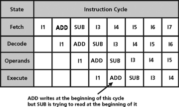
Data hazards
Data hazards are similar to resource hazards. An example of a data hazard is shown below:
is followed by
a data hazard exists if R1 is not written by the time SUB reads it. Data hazards can also occur in registers which are being used for address calculations, as shown in Figure 5.20.
Bypassing (also called forwarding) is commonly used to reduce the data hazard problem. In addition to writing the result to the register file, the hardware detects the immediate use of the value and forwards it directly to a unit bypassing the write/read operation (Figure 5.21).
There are several types of data hazards. These include:
• Read after Write – This is where j tries to read a source before i writes it.
• Write after Read – This is where j writes a destination before it is read by i, so i incorrectly gets the new value. This type of data hazard can occur when an increment address pointer is read as an operand by the next instruction.
• Write after Write – This type of data hazard occurs when j tries to write an operand before it is written by i. The writes end up in the wrong order. This can only occur in pipelines that write in more than one pipe stage or execute instructions out of order.
Branching control flow
Branch conditions are detected in the decode stage of the pipeline. In a branch instruction, the target address is not known until the execute stage of the instruction. The subsequent instruction(s) have already been fetched, which can potentially cause additional problems.
This condition does not just happen in branches but also subroutine calls and returns. An occurrence of a branch instruction in the pipeline is shown in Figure 5.22.
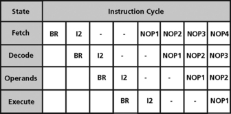
The solution to branch effects is to “flush” or throw away every subsequent instruction currently in the pipeline. The pipeline is effectively stalled while the processor is busy fetching new instructions until the target address is known. Then the processor starts fetching the branch target.
This condition results in a “bubble” where the processor is doing nothing, effectively making the branch a multicycle instruction equal to the depth of the branch resolution in the pipeline. Therefore, the “deeper” the pipeline (the more stages of an instruction there are), the longer it takes to flush the pipeline and the longer the processor is stalled.
Another solution is called a delayed branch. This is essentially like a flush solution but has a programming model where the instructions after the branch will always be executed. The number of instructions is equal to the number of cycles that have to be flushed. The programmer fills the slots with instructions that do useful work if possible. Otherwise the programmer inserts NOPS. An example of a delayed branch with three delay slots is the following:
BRNCH Addr.; Branch to new address
INSTR 4 ;Executed when branch not taken.
In a “conditional branch with annul” solution, processor interrupts are disabled. The succeeding instructions are then fetched. If the branch condition is not met then the execution proceeds as normal. If the condition is met, the processor will annul the instructions following the branch until the target instruction is fetched.
Some processors implement a branch prediction solution. In this approach, a paradigm is used to predict whether the branch will be taken or not. A cache of branch target locations is kept by the processor. The tag is the location of the branch, and the data is the location of the target of the branch. Control bits can indicate the history of the branch. When an instruction is fetched and if it is in the cache, it is a branch and a prediction is made. If the prediction is taken, the branch target is fetched next. Otherwise, the next sequential instruction is fetched. When resolved, if the proessor predicted correctly then execution proceeds without any stalls. If mis-predicted, the processor will flush the instructions past the branch instruction and re-fetch the correct instruction.
Branch prediction is another approach for handling branch instructions. This approach reduces the number of bubbles, depending on the accuracy of the prediction. In this approach the processor must not change the machine state until the branch is resolved. Because of the significant unpredictability in this approach, branch prediction is not used in DSP architectures.
Interrupt effects
Interrupts can be viewed as a branch to an interrupt service routine. Interrupts have a very similar effect to branches. The important issue in this situation is that the pipeline increases the processor interrupt response time.
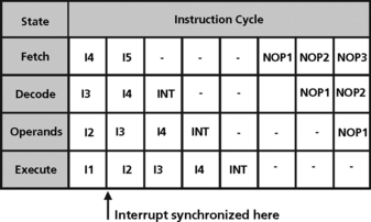
In the TI TMS320C5x DSP, the interrupt processing is handled by inserting the interrupt at the decode stage in place of the current instruction (Figure 5.23). Inserting the entire bubble avoids all pipeline hazards and conflicts. Instructions are allowed to drain as they may have changed state such as address pointers. On return from the interrupt, I5 is the first instruction fetched.
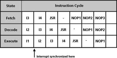
As another example of this type of interrupt processing, consider the JSR (jump to subroutine) instruction on the Motorola 5600x. JSR is stored as the first word of a two word interrupt vector. The second word is not fetched in this case (Figure 5.24).
Pipeline Control
DSP programmers must also be knowledgeable of the processor pipeline control options. There are different types of processor pipeline control. The first is called data stationary pipeline control. In this approach, the program specifies what happens to one set of operands involving more than one operation at different points in time. This style of control tracks a single set of operands through a sequence of operations and is easier to read.
Time-stationary pipeline control is when the program specifies what happens at any one point in time to a pipeline involving more than one set of operands and operators. In this method the programmer specifies what the functional units (address generators, adders, multipliers) are doing at any point in time. This approach allows for more precise time control.
Interlocked or protected pipeline control allows the programmer to specify the instruction without control of the pipeline stages. The DSP hardware resolves resource conflicts and data hazards. This approach is much easier to program.
As an example of time stationary control, consider the Lucent DSP16xx MAC loop instruction shown below:
This instruction can be interpreted as follows: At the time the instruction executes,
• accumulate the value in p in A0;
• multiply the values in x and y and store in p;
• store the value of the memory location pointed to by R0 in y and increment the pointer;
• store the value of the memory location pointed to by Pt in x and increment the pointer.
As an example of data-stationary control, consider the Lucent DSP32xx MAC loop instruction shown below:
This instruction is interpreted as follows:
• Fetch the value of the memory location pointed to by R3 and store in y and increment the pointer.
• Fetch the value of the memory location pointed to by R4 and store in x and increment the pointer.
• Store the value fetched in the above step in the memory location pointed to by R5 and increment the pointer.
• Multiply the values stored above in x and y and accumulate in A0.
Specialized Instructions and Address Modes
As mentioned earlier, DSPs have specialized instructions to perform certain operations such as multiply and accumulate very quickly. In many DSPs, there is a dedicated hardware adder and hardware multiplier. The adder and multiplier are often designed to operate in parallel so that a multiply and an add can be executed in the same clock cycle. Special multiply and accumulate (MAC) instructions have been designed into DSPs for this purpose. Figure 5.25 shows the high level architecture of the multiply unit and adder unit in parallel.
DSPs can also perform multiple MAC operations using additional forms of parallelism. For example, the C5000 family of TI DSPs have two adders—one in the ALU and another within the MAC unit, as shown in Figure 5.26. This additional form of parallelism allows for the computation of two filter taps per cycle, effectively doubling performance for this type of operation. The RPTZ instruction is a zero overhead looping instruction that reduces overhead in this computation. This is another unique feature of DSPs that is not found in other more general-purpose microprocessors.
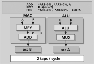
Figure 5.26 A DSP with two adders, one in the MAC unit and one in the ALU (courtesy of Texas Instruments)
The instructions in Figure 5.26 are part of a symmetrical FIR implementation. The symmetrical FIR first adds together the two data samples, which share a common coefficient. In Figure 5.27, the first instruction is a dual operand ADD and it performs that function using registers AR2 and AR3. Registers AR2 and AR3 point to the first and last data values, allowing the A accumulator to hold their sum in a single cycle. The pointers to these data values are automatically incremented (no extra cycles) to point to the next pair of data samples for the subsequent ADD. The repeat instruction (RPTZ) instructs the DSP to implement the next instruction “N/2” times. The FIRS instruction implements the rest of the filter at 1 cycle per each two taps. The FIRS instruction takes the data sum from the A accumulator, multiplies it with the common coefficient drawn from the program bus, and adds the running filter sum to the B accumulator. In parallel to the MAC unit performing a multiply and accumulation operation (MAC), the ALU is being fed the next pair of data values via the C and D buses, and summing them into the A accumulator. The combination of the multiple buses, multiple math hardware, and instructions that task them in efficient ways allows the N tap FIR filter to be implemented in N/2 cycles. This process uses three input buses every cycle. This results in a lot of overall throughput (at 10 nSec this amounts to 30 M words per sec—sustained, not “burst”).
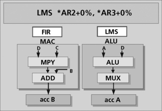
Another form of LMS instruction (another specialized instruction for DSPs), merges the LMS ADD with the FIR’s MAC. This can reduce the load to 2N cycles for an N tap adaptive filter. As such, a 100th order system would run in about 200 cycles, vs. the expected 500. When selecting a DSP for use in your system, subtle performance issues like these can be seen to have a very significant effect on how many MIPS a given function will require.
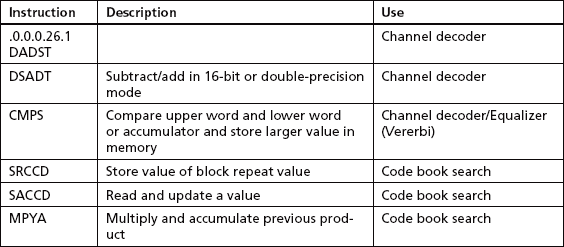
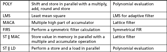
The LMS instruction on a TI 5000 family DSP works similar to a MAC (Figure 5.27). LMS uses two address registers (AR’s) to point to the data and coefficient arrays. A normal MAC implements the FIR process in the B accumulator. And, the addition of the coefficient to the tap-specific weighted error is performed in parallel, with the result being sent to the A accumulator. The dual accumulators aid in this process by providing the additional resources. The FIRS and LMS are only a few of the special instructions present on modern DSPs. Other, even higher performance instructions have been created that give extra speed to algorithms such as code book search, polynomial evaluation, and viterbi decoder processes. Each offers savings of from 2:1 to to over 5:1 over their implementation using ‘normal’ instructions. Table 5.3 lists some of the other specialized instructions on digital signal processors that offer significant performance improvements over general-purpose instructions.
Circular Addressing
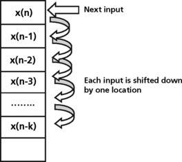
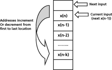
In many signal processing applications, semi-infinite data streams are mapped into finite buffers. Many DSP systems that perform a data acquisition function require a robust way to store bursts or streams of data coming into the system and process that data in a well defined order. In these systems, the data moves through the buffer sequentially. This implies a first in first out (FIFO) model for processing data. A linear buffer (Figure 5.28) requires that the delay in the filter operation be implemented by manually moving data down the delay line. In this implementation, new data is written to the recently vacated spot at the top of the dedicated buffer. Many DSPs as well as data converters such as ADCs implement a FIFO queue as a circular buffer (Figure 5.29). Circular buffers realize the delay line in a filter operation, for example, by moving a pointer through the data instead of moving the data itself. The new data sample is written to a location that is one position above the previous sample10. In a circular buffer implementation, read and write pointers are used to manage the buffer. A write pointer is used to track where the buffer is empty and where the next write can occur. A read pointer is used to track where the data was last read from. In a linear buffer, when either pointer reaches the end of the buffer it must be reset to point to the start. In circular addressing modes, the resetting of these pointers is handled using modulo arithmetic.
Some DSP families have special memory mapped registers and dedicated circuitry to support one or more circular buffers. Auxiliary registers are used as pointers into the circular buffer. Two auxiliary registers need to be initialized with the start and end addresses of the buffer. Circular buffers are common in many signal processing applications such as telephone networks and control systems. Circular buffer implementations are used in these systems for filter implementations and other transfer functions. For filter operations, a new sample (x(n)) is read into the circular buffer, overwriting the oldest sample in the buffer. This new sample is stored in a memory location pointed to by one of the DSP auxiliary registers, AR(i). The filter calculation is performed using x(n) and the pointer is then adjusted for the next input sample11.
Depending on the application, the DSP programmer has the choice of overwriting old data if the buffer becomes filled, or waiting for the data in the circular buffer to be retrieved. In those applications where the buffer will be overwritten starting from the beginning of the buffer, the application simply needs to retrieve the data at any time before the buffer is filled (or ensure that the consumed rate of data is faster than the produced rate of data). Circular buffers can also be used in some applications as pre and post trigger mechanisms. Using circular buffers, it is possible for the programmer to retrieve data prior to a specific trigger occurring. If this failure of interest is tied to a triggering event, the software application can access the circular buffer to obtain information that led up to the failure occurring. This makes circular buffers good for certain types of fault isolation.
Bit-Reversed Addressing
Bit-reversed addressing is another special addressing mode used in many DSP applications. Bit-reversed addressing is used primarily in FFT computations. In these computations, either the inputs are supplied in bit-reversed order or the outputs are generated in bit-reversed order. DSPs are optimized to perform bit-reversed addressing. Calculations that use this addressing mode such as FFTs, are optimized for speed as well as decreased memory utilization. The savings come from the software not having to copy either the imput data or the output results back and forth to the standard addressing mode. This saves time and memory. Bit-reversed addressing is a mode in many DSPs, enabled by setting a bit in a mode status register. When this mode is enabled, all addresses using pre-defined index registers are bit-reversed on the output of the address. The logic uses indirect addressing with additional registers to hold a base address and an increment value (for FFT calculations, the increment value is one half the length of the FFT).
Examples of DSP Architectures
This section provides some examples of the various DSP architectures. DSP controllers and cores are discussed as well as high performance DSPs.
Low-Cost Accumulator-Based Architecture
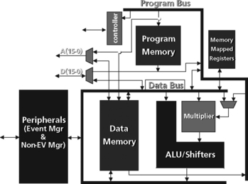
An example of a DSP microcontroller is the TMS320C24x (Figure 5.30). This DSP utilizes a modified Harvard architecture consisting of separate program and data buses and separate memory spaces for program, data and I/O. It is an accumulator-based architecture. The basic building blocks of this DSP include program memory, data memory, ALU and shifters, multipliers, memory mapped registers, peripherals and a controller. These low-cost DSPs are aimed at motor control and industrial systems, as well as solutions for industrial systems, multifunction motor control, and appliance and consumer applications. The low cost and relative simplicity of the architecture makes this DSP ideal for lower cost applications.
Low-Power DSP Architecture
The TI TMS320C55x DSP shown in Figure 5.31 is an example of a low power DSP architecture. This DSP design is a low power design based on advanced power management techniques. Examples of these power management techniques include:
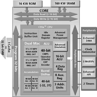
• Selective enabling/disabling of six functional units (IDLE domains). This allows for greater power-down configurability and granularity (Figure 5.32).
• Automatic turn-on/off mechanism for peripherals and on-chip memory arrays. Only the memory array read from or written to, and registers that are in use, contribute to power consumption. This management functionality is completely transparent to the user.
• Memory accesses are minimized. A 32-bit program reduces the number of internal/external fetches. A cache system with burst fill minimizes off-chip memory accesses, which prevents the external bus from being turned on and off, thereby reducing power.
• Cycle count per task is minimized due to increased parallelism in the device. This DSP has two MAC units, four accumulators, four data registers, and five data buses. This DSP also has “soft-dual” instructions, for example a dual-write, double-write, and double-push in one cycle.
• The multiply unit is not used when an operation can be performed by a simpler arithmetic operation.
Event-Driven Loops Applications
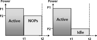
Many DSP applications are event driven loops. The DSP waits for an event to occur, processes any incoming data, and goes back into the loop, waiting for the next event.
One way to program this into a DSP is to use NOPs. Once the event occurs, the DSP can start execution of the appropriate routine (the active region in Figure 5.32). At the end of the routine, the programmer has the option of sending the DSP back into an infinite loop type of a structure, or executing NOPs.
The other option is to use IDLE modes. These are power down modes available on the C5000. These modes power down different sections of the C5000 device to conserve power in areas that are not being used. As Figure 5.32 shows, idle modes use less power than NOPs.
A DSP With Idle Modes
The TI C5000 devices have three IDLE modes that can be initiated through software control. In the normal mode of operation, all the device components are clocked. In IDLE 1 mode, the CPU processor clock is disabled but the peripherals remain active. IDLE 1 can be used when waiting for input data to arrive from a peripheral device. IDLE 1 can also be used when the processor is receiving data but not processing it. Since the peripherals are active, they can be used to bring the processor out of this power down state.
High-Performance DSP
Figure 5.33 shows the architecture of a high performance TMS320C6x DSP. This device is a very long instruction word (VLIW) architecture. This is a highly parallel and deterministic architecture that emphasizes software-based flexibility and maximum code performance through compiler efficiency. This device has eight functional units on the DSP core. This includes two multipliers and six arithmetic units. These units are highly orthogonal, which provides the compiler with many execution resources to make the compilation process easier. Up to eight 32-bit RISC-like instructions are fetched by the CPU each cycle. The architecture of this device includes instruction packing, which allows the eight instructions to be executed in parallel, in serial, or parallel/serial combinations. This optimized scheme enables high performance from this device in terms of reduction of the number of program instructions fetched as well as significant power reductions.

VLIW Load and Store DSP
Figure 5.33 is an example of a load store architecture for a VLIW DSP. This architecture contains a CPU, dual data paths, and eight independent orthogonal functional units. The VLIW architecture of this processor allows it to execute up to eight 32-bit instructions per cycle.
A detailed view of the register architecture is shown in Figure 5.34. Each of the eight individual execution units are orthogonal; they can independently execute instructions during each cycle. There are six arithmetic units and two multipliers. These orthogonal execution units are:

• L-Unit (L1, L2); this is a 40-bit Integer ALU used for comparisons, bit counting, and normalization.
• S-Unit (S1, S2); this is a 32-bit ALU as well as a 40-bit shifter. This unit is used for bitfield operations and branching.
• M-Unit (M1, M2); this is a 16 × 16 multiplier which produces a 32 bit result.
• D-Unit (D1, D2); this unit is used for 32-bit adds and subtracts. The unit also performs address calculations.
There is independent control and up to eight 32-bit instructions can be executed in parallel. There are two register files with 32 registers each and a cross path capability which allows instructions to be executed on each side of the register file.
The external memory interface (EMIF) is an important peripheral to the high performance DSP. The EMIF is an asynchronous parallel interface with separate strobes for program, data and I/O spaces. The primary advantages of the extended address range of the EMIF are prevention of bus contention and easier to interface to memory because no external logic is required. The EMIF is designed for direct interface to industry standard RAMs and ROMs.
Summary
There are many DSP processors on the market today. Each processor advertises its own set of unique functionality for improving DSP processing. However, as different as these processors sound from each other, there are a few fundamental characteristics that all DSP processors have. In particular, all DSP processors must:
To accomplish these goals, processor designers draw from a wide range of advanced architectural techniques. Thus, to create high performance DSP applications, programmers must master not only the relevant DSP algorithms, but also the idioms of the particular architecture. The next chapter will address some of these issues.
References
Wolf, Alexander. VLIW Architecture Emerges as Embedded Alternative. Embedded Systems Programming. February 2001.
Ciufo, Chris. DSP Building Blocks to Handle High Sample Rate Sensor Data. COTS Journal. March/April 2000.
Lapsley, Phil, Bier, Jeff, Shoham, Amit, Lee, Edward A. DSP Processor Fundamentals, Architectures and Features. BDTI, 1995.
Vink, Gerard. Programming DSPs using C: efficiency and portability trade-offs. Embedded Systems. May 2000.
Hendrix, Henry. Implementing Circular Buffers with Bit-reversed Addressing, Application Report SPRS292. Texas Instruments, November 1997.
1If a bus is bidirectional there will be bus “turn-around” time built-in to the latency equation. A one-directional bus has fewer transistors, which will make data accesses and writes faster. The bottom line is that the simpler the bus, the faster it will operate
2Performance improves significantly with cache up to 256KB. After that the performance benefit starts to flatten out. Once the cache reaches a certain size (around 512 KBytes) there is almost no additional benefit. This is primarily due to the fact that the larger the cache, the more difficult it is to keep track of the data in the cache and the longer it takes to determine the location and availability of data. Checking for and finding data in a small cache takes very little time. As the cache size grows, the time required to check for data increases dramatically while the likelihood of the data being found increases marginally.
3The TMS320C20 is an example of a DSP that uses this instruction.
4The Lucent DSP16xx is an example of a DSP that implements this type of instruction.
5The ZR3800x is an example of a DSP that implements this type of cache system.
6Example of this system include the TMS320C30 and the Motorola DSP96002.
7Execution predictability is a programmer’s ability to predict the exact timing that will be associated with the execution of a specific segment of code. Execution predictability is important in DSP applications because of the need to predict performance accurately, to ensure real-time behavior, and to optimize code for maximum execution speed.
9CMOS circuits consume power when they switch. By slowing the clock down to minimize switching, the power consumption in CMOS circuits goes down dramatically.
10For a complete description, see application note SPRA292, Implementing Circular Buffers with Bit-Reversed Addressing, Henry Hendrix, Texas Instruments
11For more, see Texas Instruments application note SPRA264, Using the Circular Buffers on the TMS320C5x, by Thomas Horner.