
Chapter 1
Introduction
Chapter Contents
1.1 Philosophy of Micro/Nanofabrication
1.2 The Industry–Science Dualism
1.3 Industrial Applications
1.4 Purpose and Organization of this Book
1.1 Philosophy of Micro/Nanofabrication
Microsystems technology (MST) focuses on the miniaturization of engineering systems to accommodate design specifications of small space, light weight and enhanced portability. An additional advantage of such portable systems is their wide-scale utility in distributed transducer networks. The importance of MST lies, for a large part, in the economical and technical development of innovative systems that it makes possible. The field of microfabrication technology has been established for approximately 50 years and thus it is a relatively young discipline. The first object of miniaturization was the integrated transistor, the workhorse device by means of which major new markets were created. For example, information and communication technology (ICT) relies on the technical principles of miniaturization by integrating more and more electronic functional elements into the same restricted area of a silicon die, the chip. Complementing this chip with a large data storage capacity that has fast read/write access and a high-definition display has given rise to systems which have penetrated all layers of personal and professional human lives. These types of devices are a smart combination of millions of transistors on a single chip, produced on dedicated microelectronic production lines. Transferring technological innovation into a robust and efficient production and marketing process is the secret to providing more and more computing power. The accurate line-width control during manufacturing these devices, at the micrometer or subsequently the nanometer level, is the main reason for giving this pool of associated fields concerned with the design, fabrication, assembly and testing the names micro- and nanotechnology, respectively. The very nature of these new disciplines within the engineering sciences originate from the principles of miniaturization, which was based on having an increasing number of the same circuitized components available on one die. Eventually, further and further integration allows novel functions that were originally unforeseen by conventional machining techniques. One example of such a novel microfabricated product, combining optical and electrical functions with a mechanical function at a small footprint, is an integrated optical light modulator, which we simply call a beamer in everyday life and which we consider a commodity today.
The technical methods which are used to manufacture micro products are described collectively as microfabrication techniques. Their efficiency is due to the definition of patterns in a masking layer and the subsequent parallel transfer of these accurate patterns into a functional material. During pattern transfer, the pattern is therefore copied from a mask, which carries the design features, onto or into a work piece. This work piece can be defined within a thin film or a stack of films, or the bulk of the material, which is also used as the handling platform during such a sequence of process steps. These two distinct approaches are called surface and bulk micromachining. Usually, pattern transfer is a process of at least two main steps. The first step involves the generation of the pattern, either directly by a serial write process, or by parallel patterning using an exposure through a master into a layer (usually a photosensitive polymer). This layer then acts as a masking layer for the second main step: shaping the functional material by processes such as deposition, etching or implantation. Specialists in the field generally call this layer a resist. Other modifications of the accessible areas of the work piece are of course also possible.
The continuous implementation and definition of novel fabrication techniques for modifying and transferring the patterns is key to innovation in the market place. It is this field of research and development that I would like to address in this book.
Lithographic processes have been described many times. In brief, the careful definition of process steps brought about the initial success of industrial lithography, specifically photolithography utilizing a mercury lamp with an intensity peak at a wavelength of 365 nm (UV-light) for transferring the information contained in the master into the resist. An average process sequence for a single device may contain 20–30 individual steps, some of which are considered to be the main steps of the process. This main step receives greater attention during the development of a process document. However, any set or combination of these steps may lead to a new technology.
MST is considered as less conservative than integrated circuit technology (microelectronics), because MST processes are reshaped by prototyping or the fabrication of demonstration devices instead of focussing on high-volume production. For microelectronics it is important that each process step is optimized for through-put and robustness (achieving a high yield). Costs are reduced in microelectronics manufacture due to the ability to copy a complex design in parallel from a special information carrier (photomask) hundreds and thousands of times, with the same high pattern fidelity, by simple shadow optics (exposure through a mask). This manufacturing strategy is called batch processing and is also an essential aspect of the philosophy of micro- and nanofabrication. An overview of the procedure which establishes a societal need, develops the technology and realizes an MST device is depicted in Figure 1.1.
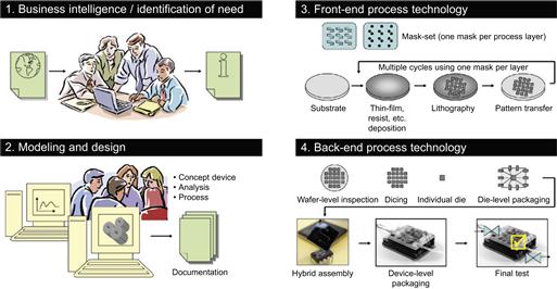
Figure 1.1 Schematic of the process from the indentification of a need to the development of batch-process technology.
Nanofabrication is a logical step to the further downscaling of the physical size of components and functional elements, often using the same machinery as microfabrication. Nanotechnology as a new discipline, however, should not be considered as simply an extension of existing techniques to smaller dimensions, but as the integration of novel functions based on an understanding of interactions at a scale of less than 100 nm. Alongside this, bottom-up manufacturing has been introduced. This approach or the previously used top-down method can be chosen, depending on the nature of the engineering problem at hand. Selection of appropriate methodology should also take into account:
(i) performance-based criteria related to the functioning of the system,
(ii) affordability of fabrication during the demonstration phase,
(iii) cost-to-performance criteria for efficient manufacture and sustainable resources during a product’s manufacturing cycle.
This is not a trivial task for scientists and product developers, particularly since all three of these groups of criteria need to be satisfied simultaneously.
Another aspect of the philosophy of micro- and nanofabrication is the concept of integration levels. The terms hybrid and monolithic integration are used, with fully monolithically manufactured systems being the most integrated. From an industrial point of view, however, the latter is not necessarily the most favourable. It is the requirements of a specific product in a market place that determine the optimal approach.
One of the key innovations during the last five decades has been the controlled deposition of thin films. Solvent-based liquid, vapour or gas phase deposition processes are now readily available in the microelectronics industry. Thin-film technology is also an important driver for the definition of materials at the nanoscale. Tuning a material’s properties allows the creation of novel applications. An introduction to nanofabrication is presented in Chapter 4 of this book. Presenting emerging nanofabrication techniques in the context of this book will allow us to draw additional attention to the paradigm shift that is now occurring in the world of production processes. Chapter 4 draws specific attention to the challenges of the positional assembly of nanoscale building blocks.
Unfortunately, at this moment it is difficult to give a clear definition of either micro- or nanotechnology. Thin-film technologies, for example, are already difficult to put into one category or the other, so it is important to clarify what one means when using the terms micro- or nanofabrication. In this context we distinguish nanofabrication from microfabrication techniques if the control of lateral dimensions can be realized precisely enough to result in features at the sub-micrometer scale. Within this framework, the structure height-to-line width ratio (aspect ratio) becomes a special measure of process performance in microsystems’ product development.
As far as MST is concerned, it is easier to give a definition of the field of work instead of defining what actually micro- or nanotechnology is. MST leads to systems-on-chip devices, including their peripheral systems, containing electronic, sensing and actuating functionality packaged within a volume of a few cubic centimeters. Hence, specifically in the USA, this field is historically referred to by the name microelectromechanical systems (MEMS) technology. Sometimes the integrated electronic circuits, sensors and actuators are referred to as the brains, eyes and arms of artificial systems, an expression that has been used by Huff in his tutorial report on MEMS technology [1]. Optical switching and attenuation components are another large group of devices which benefit from the research and development into micro- and nanofabrication principles. The manufacture of microsystems involves a variety of precision engineering techniques, combined with silicon surface micromachining techniques. The first group of techniques (e.g., dicing, laser cutting, lamination, thermal compression bonding) enables the separation or assembly of components, while micromachining is dedicated to the integration of the three sub-functions from the electrical, mechanical and optical domain at the microscale.
With respect to the choice of materials, silicon is the most abundantly used material in miniaturization, although fabrication techniques should be evaluated for substrate materials other than silicon. A systematic overview of basic microfabrication techniques is given in Chapter 2.
The next three sections will give an overview of the content of this book. I also wish to present some guidelines on how this book may be used educationally as part of a course concerned with micro- and nanofabrication technology and its impact on industrial applications.
1.2 The Industry–Science Dualism
It is interesting that today, in the year 2011, we talk about knowledge societies. It was not long ago that productivity and industrialization were considered to be the key to a better health and education system, and hence a better life. In this section, we would like to discuss briefly the process behind the accumulation of knowledge, which is important for feeding existing industries such as raw materials industries (e.g., mining and farming), manufacturing, or services industries (dealing with law, medicine or the distribution of goods). Recently a new type of industry has been added to the three existing sectors: the knowledge industry, which deals with research, design and development. Knowledge creation is a skill one can teach. Children, teenagers and young adults all around the world are taught that knowledge is a driving force for building their careers. Adults are the workforce for the many successful businesses, including multinational corporations and governments. Industrial organizations cannot exist without mining accumulated knowledge or the application of business intelligence.
In contrast with an academic (pre-competitive) knowledge creation, however, industry points towards the economic valuation of knowledge: knowledge had to become a marketable product. Hence, it became a common practice to apply for patents.
A patent grants the owner the exclusive right to commercialize products or services. The idea or process being protected by a patent must contain an innovative step, and the disclosed information must be industrially applicable when the patent application is filed. Of course, if such an idea is disclosed it is already branded as intellectual property (IP), but a patent or trademark must be first registered and granted before the knowledge can be effectively traded on the market. This is a concept inherently different from science as an academic occupation. The right that one receives to commercialize the disclosed knowledge is a non-tangible asset of a business, which can be very valuable.
With respect to the development of micro- and nanofabrication techniques for industrial applications, it is important that we understand how IP is first generated and secondly traded. The latter is important if one wants to sell the accumulated knowledge through technology transfer. Not-for-profit organizations such as universities can be important trading partners in this knowledge industry. This approach may be easier understood if one realizes that a marketable, tangible product does not normally consist of only one invention. Several, often at different developmental stages, have to be combined to be able to form one product. Obviously, higher complexity will increase the number of components required, which means that the involvement of other market players becomes increasingly important for the effective realization of the product. For this type of development, a relatively new term has been introduced to business models: the concept of open innovation. Although many companies will still be able to draw good profits from closed innovation, the complexity of systems in the modern world asks for more flexibility.
If you are not familiar with IP rights and their generation, the website of the World Intellectual Property Organization (WIPO) is a good starting point for finding out, and also for continuous updates on the procedures [2]. For details of the patent application process, and the legal rights attached to a patent, other sources are better, e.g., for Europe it may be helpful to check specific guidelines concerned with European patents [3, 4]. There are also guidelines on this topic for other countries and regions. Remember that ordinary people, as well as large organizations can apply for a patent, and many inventors use this instrument to pass on their knowledge to avoid the need for large investments. Large investments of the order of millions of US Dollars are very common for the initial steps of product development and scientific publication of the finding may compromise the inventor’s commercial rights to it, but a patent can be applied for and maintained through various stages of this development process without significant costs. Also, inventors in small and medium-sized enterprises as well as researchers in the academic community can create businesses in this knowledge industry, by making use of patent protection as a business instrument by first attaining the commercial rights to their IP and then selling it to create their own knowledge-generating businesses. If financially sustained with the appropriate authorities, a patent is granted for 20 years, which in today’s fast life-style is probably a reasonable head start over possible competitors.
How is IP initially generated? Of course, one immediately wishes to say: IP is generated by good ideas! However, that is not sufficient according to the description above, which suggests a patent is only granted if there is an inventive and an innovative step as well as an industrial application, which means, that quickly the inventor finds him- or herself in the area of technology. In the field of technology, the design plays a major role. Replacing the word technique in the field of technology with design, we can also formulate a guideline for exercising the knowledge presented in this book by a free translation of a Dutch quote taken from van den Kroonenberg lecture notes in 1998:
“Design is the process, which is directed to combine the knowledge of the existing laws of nature in such a way that it increases the efficacy of collection of knowledge in relation to another matter on the reason of need, demands and wishes of a human being.” [6]
How is a human being, an inventor, actually collecting natural laws to realize the process of knowledge generation, and how is an inventor making use of it in a design process? The guideline, unfortunately, does not give direct answers to these questions. This book is dedicated to the complexity of such design processes in the use of microfabrication techniques in industry.
1.3 Industrial Applications
Since knowledge from technology may have multiple applications across several different working fields the term “industrial applications” is specifically chosen to underline the potential of microfabrication for use in other research fields and marketable solutions. From a business point of view these multiple applications would be furthered by licensing agreements, which would allow the technology to be used commercially for a specific purpose by different industrial players.
To be able to clarify the definition of industrial players one needs to have a closer look at the creation of markets. Based on a simple definition in marketing we can call the total population “a market”, but the “potential market” is the portion of the total population who have an interest in acquiring the product or service under consideration. In this definition the available market covers the sub-population that has sufficient money to afford the product. The latter may shrink to a qualified market, which represents the sub-sub-population that is eligible to buy the product. This qualified available market may subsequently be reduced to the target market, which is the market share that the company has decided to serve with its product (sub-sub-sub population). Finally, the penetrated market remains, which is the sub-sub-sub-sub-population of those in the market who have actually purchased the product. This final sub-sub-sub-sub-population is difficult to capture at the very early stages of a product development cycle, particularly for a novel and complex technology, which has yet to prove its worth. This is often referred to as the technology gap between science and industry. One way to approach this is the reduction of risks by developing a product over several stages that deliver a proof-of-concept for each stage. Early stage investments into a rising technology star, obviously, may promise very attractive profits.
Figure 1.2 conceptually presents the three possible market drivers, which divide the market population into three sub-populations (markets) that are driven by their specific needs, wishes and desires. At a very early stage of business it is difficult to propose that these markets could mix and merge. Currently, few publications exist that enlighten us on the mechanism of successful business development in a knowledge society [5]. I would like to suggest that at this initial stage of considering a technology–product match it may be possible to analyze these three drivers individually. With high-tech products, the three areas may merge eventually if a real need has been identified, and making products to satisfy this need is more likely to produce a satisfying return-of-investment than if a specific need is not identified.
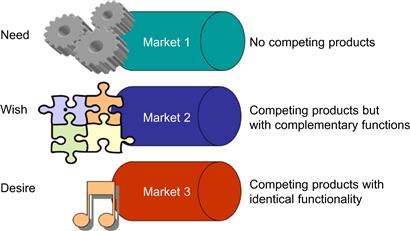
Figure 1.2 Drivers for gaining market shares.
1.4 Purpose and Organization of this Book
This book is a study book. A study book should not only make you buy the book based on an interesting title but should also satisfy your needs; in this case, a need to learn more about microfabrication for industrial applications. This book is not a thesis on the definition of the economical value of microfabrication nor a dedicated technology handbook for specialists. The focus is micro-nanofabrication in innovative industrial areas, such as the field of (bio)medical applications.
Chapter 2 presents an overview of the basic process technologies of contemporary microfabrication. Chapter 3 extends this to broaden the range of materials being used, and considers processes that specifically aim at three-dimensional microstructures. Chapter 4 is an introduction to the terminology of nanotechnology, and an overview of the development of nanolithographic techniques that can pattern features less than 100 nm in width. Those which can produce large-scale, highly ordered pattern arrangements are of especial interest. The latter are often referred to as meta-materials.
Chapter 5 briefly reflects on the components and techniques of micromechanical transducers. Chapters 6 and 7 give an introduction to the application of microfabrication in the field of bio-chemical sensors and microfluidic Lab-on-a-Chip technologies, respectively. Chapter 8 provides the reader with a case study of microfabrication research dedicated to the drug delivery market. This example of desk research guides the reader through a commonly applied approach in the engineering sciences: knowledge accumulation and reduction of risk by applying a systematic design analysis. Finally, Chapter 9 gives some reflective comments and conclusions concerning the safety of micro- and nanotechnology and nanoparticles in particular. This last chapter also provides the reader with an overall conclusion to the book.
We will discuss fields of applications and introduce specific cases, which may have already entered the market, in the various chapters. Many examples of science-based innovation utilizing microfabrication can be found in the health sectors and a specific example is discussed in Chapter 8. Product development cycles are particularly long (>10 years) in the medical devices industry due to the necessity for devices that function robustly, to a high safety standard, because they are to be used in close vicinity to the body or inside it. Due to my personal research interest in the medical devices’ sector, particular attention will be paid in the book to the opportunities for micro- and nanofabrication to play a part in the manufacture of novel implants, diagnostic and therapeutic systems. Nevertheless, some microfabrication applications will be also presented across other markets to indicate the variety of industrial perspectives which are possible.
The book contains case studies for students in the engineering sciences and for non-engineering specialists interested in this specific field of engineering. They reflect the current state-of-the-art of microfabrication in industrial applications, and seek to interest the student in the more advanced literature that is beyond the scope of this book. The book also provides an introduction for technology managers who are possibly experienced in business but less so with the terminology in the emerging field of micro- and nanofabricated industrial applications. For a specialist, e.g., a starting PhD student from the natural sciences or another monodisciplinary background, including the social or business sciences, who wishes to cross boundaries and enter the field of MST, this book may serve as an initial reference source on applications with a highly cross-disciplinary nature. Advanced microfabrication books, and the scientific and patent literature often discuss sophisticated theory of microfabrication technologies, making them less accessible for non-specialists. This book hopes to provide a starting point in an educational engineering course positioned at the end of the first year or beginning of the second year of a bachelor study program. Therefore, this book serves as an introductory source in the field of microfabrication technologies and its industrial applications.
REFERENCES
1. Huff M. MEMS fabrication. Sens Rev. 2002;22:18–33.
2. http://www.wipo.int/portal/index.html.en, World Intellectual Property Organization, 2011 (accessed 04/04/11).
3. Wild J, ed. Patents in Europe 2008: Helping business compete in the global economy, iam-magazine. Globe White Page Ltd 2008.
4. How to Get a European Patent: Guide For Applicants. European Patent Office, The Hague, The Netherlands, 2007.
5. von Raesfeld Meijer AM. Technology transfer: Preaching to the converted or seducing the disbelievers. In: de Laet MK, ed. Amsterdam: Knowledge and Society; 2002;127–151. Research in Science and Technology Studies: Knowledge Technology Transfer. vol. 13 ISSN 0278-1557.
6. van den Kroonenberg, Methodisch Ontwerpen, Technische Hogeschool Twente, Afdeling der Werktuigbouwkunde, Vakgroep Ontwerp- en Constructieleer, 1998, page 1, identification number WB.83/OC-12461.