2
The Uses of Electrostatics
Each topic discussed below is a sophisticated discipline in itself. The purpose of this chapter is to show where actual use of electrostatic analysis is involved in actual structures. Section 2.1, on basic circuit theory, is included because this is a discipline based on electrostatic (and magnetostatic) approximations whose use is implied in the functioning of the various structures discussed in subsequent sections.
2.1 Basic Circuit Theory
The speed of an electromagnetic wave in a vacuum (and essentially the same number in air) is 3 × 10⁸ m/s. A radio wave with a frequency of 1 MHz (one million cycles per second) has a wavelength of
If we are dealing with frequencies in this range or lower and with distances of, say, ≤1 ft, then we can ignore the propagation times along wires connecting various components and we can idealize components by pretending they’re infinitely small.
These assumptions allow us to define a branch of electrical science known as circuit theory, in which wires are ideal, lossless equipotential surfaces, with infinitely high signal propagation speed. This lets us define a list of components which are characterized by voltage–current terminal conditions.1,2 Although we're introducing simple circuit theory only because some of its tools will be useful going forward, in principle all of circuit theory is a topic in electrostatics (and magnetostatics).
Circuits are composed of interconnected components and obey two basic laws known as the Kirchhoff voltage and current laws: (1) Kirchhoff’s voltage law states that the total voltage drop around a closed loop in a circuit is zero; (2) Kirchhoff’s current law states that the total current flowing into (or out of) any point, or node, is zero.
For our purposes, we will be dealing only with simple circuits and four basic components (the standard symbols for these components are shown in Figure 2.1):
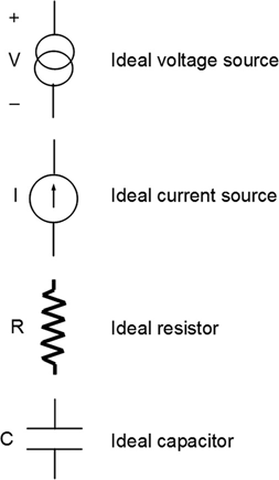
FIGURE 2.1 Four basic circuit elements.
-
The Ideal Voltage Source. This is two-terminal device with a defined voltage drop, or potential difference (and polarity), between its terminals. The ideal voltage source can supply (source) or absorb (sink) energy depending on the direction of the current through it. The ideal voltage source can never be shorted-circuited (its terminals cannot be connected to each other) because this would cause a violation of Kirchhoff’s voltage law. When the current through a voltage source is flowing into the positive (+) terminal [and out the negative (−) terminal], the voltage source is absorbing energy. When the current is flowing into the – terminal (and out the + terminal), the voltage source is delivering energy. The rate of energy absorption (or delivery) is the power
(2.2)
-
The Ideal Current Source. This is two-terminal device with a defined current (and polarity) flowing through it. The ideal current source can supply or absorb energy depending on the polarity of the voltage across it. The ideal current source can never be open-circuited because this would cause a violation of Kirchhoff’s current law. When the terminal with outflowing current is positive (and the terminal with current inflowing is negative), the current source is supplying power, and vice versa. Again.
(2.3)
-
The Ideal Resistor. This is two-terminal device whose resistance R is defined by Ohm’s law, where the ratio of the voltage across the resistor’s terminals to the current flowing through it are expressed as follows:
(2.4)
When current is flowing into the positive terminal (and out of the negative terminal), the resistor is absorbing power. A resistor cannot deliver or store power; rather, it dissipates power as heat:
(2.5)
-
The Ideal Capacitor. This is two-terminal device. From Chapter 1, the definition of capacitance is
(2.6)where Q is the charge stored on an electrode of the capacitor when V is the voltage across the capacitor's terminals.

The current flowing into (and out of) a capacitor is the rate of change of charge on the capacitor's electrodes:
This equation is taken as the defining circuit equation of a capacitor. It may be inverted to express the voltage in terms of the current:
The limits of integration (or boundary conditions in the case of the derivative equation) are discussed below.
A capacitor neither absorbs nor delivers power. It can, however, store energy (in the electric field), as described in Chapter 1:
Several examples (and further definitions) will complete our very abbreviated and truncated introduction to circuit theory.
Figure 2.2a shows a very simple circuit. A resistor is connected to an ideal voltage source. The circuit consists of one closed loop, so only one current (I) can be defined. The direction of the current is arbitrary, but it is conventional to define the direction of current as leaving the + terminal of a voltage source. The formal Kirchhoff voltage equation for this circuit is as follows,where Vr is the voltage across the resistor:
Substituting Ohm’s law for the resistor voltage and noting the proper current direction conventions, we obtain
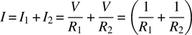
Figure 2.2b shows a simple circuit with two resistors, R 1 and R 2. These resistors are connected in series (a connection where the currents flowing through both resistors are identical). Again, there is only one current path, with current I. Writing Kirchhoff’s voltage law, we have
In the circuit shown in Figure 2.2b there are three possible places to label a voltage, or three nodes. Since only voltage differences are physically meaningful, however, it is convenient to arbitrarily label one of the nodes as the zero-, or reference or ground, voltage node, and then the other (two) nodes are understood to be voltages with respect to the reference node.
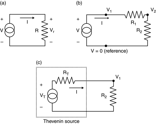
FIGURE 2.2 Some simple circuit examples using voltage sources.
Voltage V 1 is, by the definition of a voltage source, equal to V. Voltage V 2 is known because the current I is known:
Voltage V 2 is identically the voltage across R 2. The voltage across R 1 is found either as IR 1 or V 1 − V 2.
Although the ideal voltage source is an important abstraction for circuit models, it does not exist in the real world. All real voltage sources have some internal losses. Resistive losses can be modeled as resistors in series with the ideal voltage source. The resulting compound element, shown in the dashed lines in Figure 2.2c, is called a Thevenin equivalent voltage source. The internal connection between RT and VT is not accessible.
Since Figure 2.2c is identical, circuitwise, to Figure 2.2b, there is no need to re-solve the circuit equation for the current. There are, however, some important interpretive distinctions:
- Since RT cannot be changed, there is a maximum current that a Thevenin source can supply. This is the current in Figure 2.2c (or Figure 2.2b) when R 2 = 0.
- There is no paradox created by shorting-circuiting (connecting together) the two terminals of a Thevenin source.
- When a Thevenin source is supplying power to an outside resistor (or resistor network), it is dissipating power internally in RT . A Thevenin source will become hot when it is being used.
- An open-circuited (with nothing connected to it) Thevenin source is not dissipating power.
Figure 2.3 shows several simple examples using current sources.
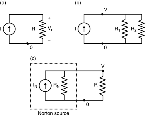
FIGURE 2.3 Some simple circuit examples using current sources.
Figure 2.3a shows an ideal current source connected to a resistor. There is only one (nonreference) voltage point (node) and
Figure 2.3b shows two resistors connected in parallel (where the voltages across both resistors are identical). Writing Kirchhoff’s current law at the voltage node V, we have
As in the case of voltage sources, ideal current sources also do not exist. A real current source, called a Norton equivalent source, is represented by an ideal current source in parallel with an internal resistance:
- Since RN cannot be changed, there is a maximum voltage that a Norton source can supply. This is the current in Figure 2.3c (or Figure 2.2c) when R goes to infinity (an open circuit).
- There is no paradox created by opening (leaving unconnected) the two terminals of a Norton source.
- When a Norton source is supplying power to an outside resistor (or resistor network), it is dissipating power internally in RN . A Norton source will become hot when it is being used.
- A short-circuited Norton source isn't dissipating power.
It can be shown that, insofar as the external circuit is concerned, it is impossible to tell whether the real source “inside the box” is a Norton or a Thevenin source, provided that
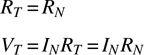
Figure 2.4 shows a Thevenin voltage source connected to a capacitor.
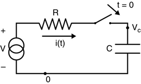
FIGURE 2.4 Simple RC circuit.
A new circuit element, the switch, has been introduced in this figure. The figure indicates that the switch is closed (i.e., a connection is made) at time t = 0. For t < 0 there is no connection. There is no current path, so I = 0. But what about VC ?
Since C is an ideal capacitor, it will retain charge on its electrodes (absent a discharge current path) forever. If there is charge Q on the electrodes, then our basic definition of a capacitor tells us that
There is no way of deriving or calculating this value of VC . It is an initial condition that we must be given.
At t = 0 the switch is closed and we can write Kirchhoff’s voltage equation
We can convert equation (2.19) to a differential equation by taking the time derivative of both sides. Since the voltage across an ideal voltage source never changes, its time derivative must be zero:
This equation may be solved by integration:
We now know the form of the solution, but we aren't finished until we can specify the initial current i(0).
We knew VC before t = 0, when it was a given piece of information. Suppose that at t = 0, VC suddenly changes value. This implies that the time derivative of the capacitor voltage dvC /dt is, at that instant, infinite. In turn, this means that the current through the capacitor, using equation (2.7), is instantaneously infinite.
Since the current through the capacitor is identical to the current through the resistor and the voltage source, we conclude that the resistor is instantaneously dissipating an infinite amount of power that the voltage source is supplying. This conclusion is physically unacceptable. This leads us to a “law” of circuit theory: The voltage across a capacitor (in the circuit theory abstract world) cannot change instantaneously.
If, for example, the capacitor had zero voltage before the switch was thrown, at the instant that the switch is thrown the capacitor voltage would remain zero. At t = 0, if there is zero voltage drop across the capacitor, then the instantaneous current is defined by the voltage source–resistor circuit
and therefore
The product RC in equation (2.23) has the units of time, and is usually defined as the time constant of the RC pair
so that
The voltage across the capacitor is simply the voltage source V minus the voltage across the resistor:
Figure 2.5 shows the voltage and current versus time for the capacitor. At t = 0, the uncharged capacitor briefly appears as a short circuit. For t large (as compared to the time constant) the capacitor appears as an open circuit. After several time constants the switch may be opened and the capacitor will remained charged at voltage V until or unless another opportunity for current flow is provided.
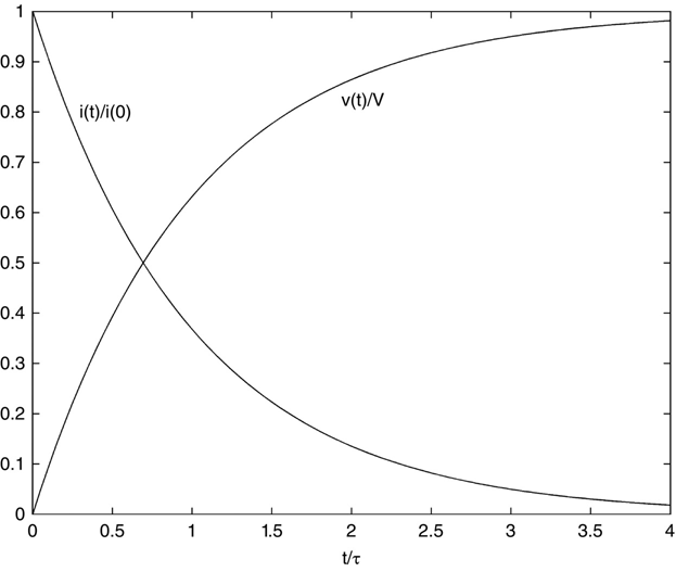
FIGURE 2.5 Voltage–current response of simple RC circuit.
Before t = 0, if the capacitor had been charged to a voltage V C0, then the preceding equations would be modified to
and
If the capacitor is fully charged (to V), the switch is opened and then a new resistor (R 2) is connected across the capacitor at time t 2, by following the same analysis as above:
According to this analysis, a capacitor is never fully charged to a connected voltage. In later chapters we will be considering capacitors charged to some specified voltage. This may be construed to mean that a capacitor was connected to either (1) a charging voltage for so many time constants that the error is negligible or (2) a higher voltage and then disconnected at the right time as the voltage swept past the desired charging voltage.
This abbreviated introduction to circuit theory has ignored several basic circuit elements, including the inductor –– an idealized coil of wire that stores energy in its magnetic field when current flows through it. This omission has, in turn, left us without a definition or explanation of resonance and resonance frequencies.
The most significant omission in this chapter is any discussion of sinusoidal alternating current (AC) analysis. This is a marvelously easy-to-present exercise in operational calculus that leads to many common applications of circuit theory (home electricity included) in the sinusoidal steady state, an important concept of which concerns impedance. Impedance is a property of circuit elements that is a generalization of resistance to include frequency-dependent effects of capacitance and/or inductance. An impedance can dissipate energy and/or cyclically store and release energy.
2.2 Radio Frequency Transmission Lines
This is a brief introduction to transmission line theory that is presented in handbook format, with only the necessary equations, with no supporting derivations. There are many transmission line texts available for learning more about the subject.3,4
Electrical transmission line theory is not an electrostatics topic. The transmission line equation is a one-dimensional wave equation and the study of transmission lines is the study of waves propagating on a transmission line. However, the properties of the typical propagating mode on a transmission line can all be calculated directly from the capacitance of the line (per unit length); this capacitance is the same as all other capacitances and is found from the stored electric field energy or the charge on the conductors. From the perspective of calculating transmission line properties, therefore, we can do our work in the electrostatic domain.
A transmission line is a length of two or more conductors with a net zero flow of current across a cross section of the line. Let us begin with a two-conductor line. Assume that the line is lossless and that there are no magnetic materials present. We will, however, allow for dielectric materials.
Some typical transmission lines are shown in cross section in Figure 2.6.
The coaxial line shown has concentric cylindrical conductors (i.e., round conductor cross sections). This is not a necessary attribute of coaxial cable, although this is by far the most typical construction. What is special about the coaxial cable is that since the currents in the two conductors are equal in magnitude and opposite in direction, no electric or magnetic fields are present outside the coaxial cable.
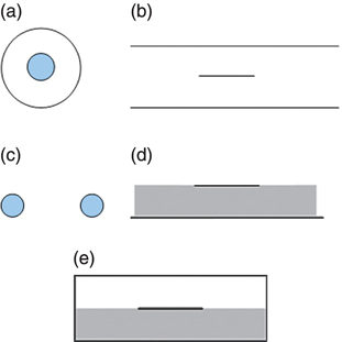
FIGURE 2.6 Some common transmission line cross sections: (a) coaxial cable; (b) stripline; (c) open-wire line; (d) open microstripline; (e) boxed microstripline. Note that there is nothing necessarily micro about the microstrip line –– the name is historical.
While the open wire line also has equal and opposite conductors flowing in the two lines, the electric and magnetic fields extend to infinity. The stripline (and microstripline) might actually be a form of coaxial cable, or it might be an open system with fields extending to infinity.
Stripline is typically built using a uniform dielectric, microstripline has a dielectric (K > 1) material in only part of the cross section. Construction of the line is easy to visualize from the picture of the line. The microstripline is different from the other lines shown because it has a nonuniform cross section and its properties will require some special consideration.
Both stripline and microstriplines typically have sidewalls of the outer conductor. The reasons for including these sidewalls are to totally contain the line's fields, prevent incursion of other fields, and provide structural support. In many cases these sidewalls are far enough away that they don't contribute to the electrical properties of the lines –– that’s why it is common to omit them in drawings. The approximation “far enough away,” however, should be examined when calculating the properties of these lines.
At frequencies low enough for waveguide modes to be cut off, the only propagating mode on a transmission line is the transverse electromagnetic (TEM) mode. In this mode, the electric field lines are transverse to the line length (i.e., in the plane of a cross section) and the magnetic field lines wrap around the conductors and are also in the plane of a cross section of the line. This mode propagates at all frequencies down to direct current (DC) (0 frequency). At DC, the electrostatic properties of the line are the properties of the TEM mode, the properties that we are interested in.
A uniform lossless transmission line operating in TEM mode has a capacitance C and an inductance L per unit length. Finding C is a two-dimensional (2d) problem even though C is a three-dimensional (3d) parameter; all electric field lines are in the cross-sectional plane. Without proof or derivation here, we'll assert that the wave propagation properties of the line arise completely from L and C. These properties are the characteristic impedance of the line

and the wave speed
The characteristic impedance is an impedance that, when connected to one end (terminating) of the line, will be the impedance measured at the other end of the line. This is unique because most terminating impedances will result in an impedance at the other end of the line that is a function of the terminating impedance, the frequency of the applied voltage, and the length of the line –– at all frequencies greater than zero (DC). Also, terminating a line in its characteristic impedance is equivalent, insofar as the input impedance and the voltage and current along the line are concerned, to having an infinite length of line.
A lossless transmission line may be modeled entirely using the distributed capacitance and inductance (per unit length) of the line. The characteristic impedance of a lossless line is, however, entirely resistive. At first blush this seems to be a mistake –– a resistor dissipates energy when a voltage is placed across it, so how can a structure consisting entirely of nondissipative capacitors and inductors be described by a resistance? The answer to this is that the characteristic impedance of a line is what is “seen” when you apply a voltage to the beginning of a line that extends to infinity. In this case the traveling wave along the line is always advancing toward (but of course never reaching) infinity, and the voltage source at the beginning of the line “sees” energy disappearing. Terminating the line at a finite length with a resistor whose value is equal to the line's characteristic resistance results in actual energy dissipation (the resistor becomes hot) but the voltage source at the beginning of the line cannot distinguish between an infinite length line and a terminated finite length line.
Maxwell’s equations tell us that a wave on a line with an air (or vacuum) dielectric will propagate at the speed of light v0. From equation (2.31), we obtain
This means that C is the only parameter needed to determine everything that we need to know about a (lossless) transmission line.
If a transmission is uniformly filled with (or embedded in) a dielectric of relative constant K, then the capacitance is scaled (from the value with an air dielectric) by K. The inductance, however, doesn't change; it is calculated from equation (2.32) for the same structure assuming that K = 1.
The microstripline doesn’t strictly operate in a TEM mode. At low frequencies (starting at 0 frequency, DC) however, the line will operate in a very TEM-like mode known as the quasi-TEM mode. The capacitance is calculated for the structure as given, and the inductance is calculated for the same structure with no dielectric material present. Since the capacitance value will be somewhere between the all-air capacitance value and an all-dielectric capacitance value, the wave velocity will also be between the all-air and all-dielectric values. A dielectric value K that, uniformly filling the space, would produce this wave velocity (and line capacitance), is referred to as the effective dielectric constant value of the structure.
Currents along the conductors of a transmission line will show the same distributions as the charge densities found in the examples in this book. In the case of a coaxial cable composed of concentric round lines, the symmetries of the geometry dictate that there be no current, or charge density, variations. In all other geometries, however, there definitely are variations. This is an important parameter to study because Ohmic (resistive) losses along a line depend (in the cross section) on the square of the current density. In other words, two different geometry lines can have very different losses (per unit length) even though they are created using the same materials and have the same cross-sectional conductor dimensions and conductor thicknesses.
Another parameter that enters into the loss calculation is the radiofrequency (RF) skin effect, which is a frequency-dependent effect that prevents currents from penetrating deeply into a real conductor. The RF skin effect is definitely not an electrostatic parameter and is outside the scope of this book.
Transmission lines are important for carrying RF signals. It is necessary to calculate the capacitance of transmission line structures to design transmission lines. When nonenclosed, or open lines are placed near one another, signals will couple. Again, a capacitance calculation is necessary to describe this coupling.
As digital signaling speeds increase, the pulses shorten and surprisingly short connection paths behave as transmission lines. An example of this is the multiline circuitboards used in, say, portable cellphones. These circuit boards must be modeled as complex transmission line structures and properly designed so that the shape of the digital pulses is not compromised and interline coupling is understood and controlled.
2.3 Vacuum Tubes and Cathode Ray Tubes
The first 70 years or so of electronics technology contain many examples of generating and controlling the flow of electrons in a vacuum. These include the use of vacuum tubes for general electronics and cathode ray tubes (CRTs) for displays. Both of these devices have been phased out by solid-state devices. Some electron beam devices, such as the scanning electron microscope (SEM), remain in use.
Design of electron beam control systems is a classical electrostatics project. Beam currents are typically low enough that distortion of the electric field by the electrons is ignored. This means that the overall problem decouples into two separate problems: the electrostatic problem of describing the potentials and fields for a given geometry and electrode voltages, and then description of electron trajectories as a function of launch conditions and the electric field. In all cases a high vacuum is maintained in an enclosed volume. This makes electron trajectory calculation an exercise in Newton’s laws, circumventing the need to consider scattering by a background gas, and at the same time avoids gas breakdown.
One technique for launching electrons into a vacuum is called thermionic emission. A thin wire filament is heated (as in an incandescent lightbulb) hot enough to glow.5 When a metal is heated, the conduction band electrons (the electrons that are free to move –– i.e., the electrons responsible for electric current flow in metals) become very energetic. Some of them will acquire enough energy to “boil off” the surface of the metal into the surrounding vacuum. When Thomas Edison placed a metal electrode in the vacuum enclosed along with the filament, he collected these electrons with a positive potential; this is now called the Edison effect.6
Figure 2.7 shows Edison’s structure. Because there are two elements, the filament and the anode (plate), this device is called a vacuum tube diode. Edison noticed that when the anode is positive (biased positive) with respect to the filament (as shown in Figure 2.7), current (I) flows. However, if the polarity of the plate voltage is reversed, so that the plate is biased negative with respect to the filament, no current flows. This was early evidence that current in metals is carried by some sort of particle that carries only a negative charge. For historical reasons, since current flow was defined as the movement of positive charge, even though the electrons flow from the filament to the plate, the electric current flow is from the plate to the filament. This subtlety often causes consternation in beginning engineering students, but is a perfectly workable system with no contradictions.
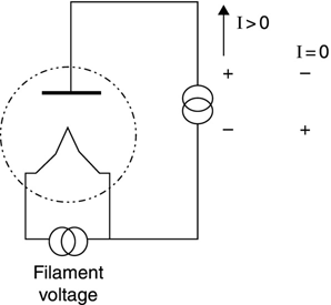
FIGURE 2.7 The vacuum tube diode.
Since this diode will pass current in only one direction, it can be used to convert alternating current to direct current. This application is known as rectification, and the vacuum tube diode is often called the vacuum tube rectifier.
Figure 2.7 is a schematic representation of a vacuum tube diode. In practice, the filament is usually a length of wire mounted at (and connected to) either end. The anode evolved from being the simple plate of Edison’s early experiments to being an open cylinder surrounding the filament. The term plate lived on, however, and is synonymous with the term anode in vacuum tube electronics.
Around 1907, Lee De Forest heralded in the era of electronics with the invention of the vacuum tube triode.7,8
De Forest added a third element to the structure: a metallic cylinder made of porous mesh between the filament and the plate. When this cylinder, called the grid because of its appearance, is biased slightly negative with respect to the filament, it lowers the local electric field and reduces the current flow between the filament and the plate. The grid itself would not collect any electrons because of its bias polarity; hence there is no grid current. If the grid is made negative enough, it would actually reduce the plate current flow to zero, or cut off the current. For small variations in grid voltage about a nominal reduced-current level (the bias point), variations in grid voltage would cause corresponding variations in plate current. The grid and its connections are shown symbolically in Figure 2.8.
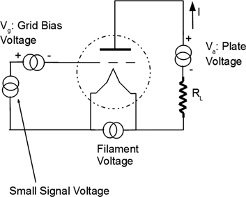
FIGURE 2.8 The vacuum tube triode.
If a load resistor (RL in Figure 2.8) is placed in series with the plate voltage supply, the plate current is reduced somewhat by the Ohmic voltage drop across this resistor. Small voltage variations in the grid voltage cause variations about the nominal value of the plate current, which, in turn, cause voltage variations across the load resistor.
What is happening here is that a small signal voltage superimposed on the grid bias voltage, which requires zero power because there is no grid current, is causing a corresponding voltage variation in the load resistor –– which in turn is dissipating power. A power amplifier has been built, and the age of electronics has begun.
There have been many advances in vacuum tubes, including (1) the indirectly heated cathode to reduce the effects of having an AC voltage on the filament; (2) a second grid between the first (control) grid and the anode to reduce anode–cathode capacitance that limits frequency response; and (3) a grid near the anode to reduce effects of secondary emission (electrons crashing into the anode and causing new electrons to be emitted by the anode). This final structure, the vacuum tube pentode, was the workhorse of the electronics industry for decades.
The cathode ray tube (CRT) is a vacuum tube with a filament, a cathode, a control grid, and an anode but also has other elements and a purpose entirely different from that of the vacuum tubes described above.
Figure 2.9 shows, schematically, an electrostatic CRT. Connecting wires are not shown; they are typically brought in at the end of the neck of the tube (the left end in Figure 2.9). An exception to this is the anode voltage, which is typically brought in near the anode, or screen, end (the right end in Figure 2.9).
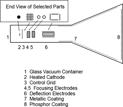
FIGURE 2.9 The electrostatic cathode ray tube.
The labeled components and their functions are as follows:
- The glass bottle defines the structure and holds the vacuum.
- The heated cathode is a source of electrons.
- The control grid controls the current flow in the electron beam. Since the CRT is an electronic display, the control grid controls the brightness of the spot of light that will be created on the screen.
- The focusing electrodes are cylindrical electrodes biased so as to cause the beam of electrons passing through them to bunch up, thus minimizing the cross-sectional area of the electron beam at the anode.
- Two or more focusing electrodes ensure better focusing control.
- There are two pairs of deflection electrodes. A potential on the vertical (in Figure 2.9) pair causes a horizontal deflection of electrons; a potential on the horizontal pair causes a vertical deflection of electrons. By setting these potentials, any point on the screen could be illuminated by electrons.
- A metalized coating on the inside of the glass that is set to the anode voltage and creates an accelerating field for the electrons toward the screen.
- A phosphor coating on the inside of the glass. Certain ceramic materials called phosphors emit light when struck by energetic electrons. This phosphor layer is also set at anode potential.
The CRT structure as shown was used for oscilloscopes and small television (TV) screens. Over the years, as TV screens became larger, anode voltages higher and manufacturing techniques more mature, the focusing and deflection electrodes were replaced by a magnetic structure (the yoke), a compound doughnut-shaped set of coils that is mounted around (on the outside of) the neck of the tube.
Manufacturing of the CRT became so well controlled and inexpensive that even the extension of the technology to the three-electron-gun shadow-mask tube for color TVs allowed this device to become a household item.9
2.4 Field Emission and the Scanning Electron Microscope
When the electric field at the surface of a metal then is high enough, and the field is directed so as to sweep electrons away from the metal, electrons are emitted from the metal by a process called tunneling. There is no way to explain tunneling in classical physics concepts. Tunneling is a quantum mechanical phenomenon. The electrons do not literally “tunnel through” the surface of the metal; they simply appear outside the surface. Historically, an accurate description of electron tunneling, called the Fowler–Nordheim equations after the developers of this description, was one of the early successes of the then new quantum theory early in the twentieth century.10,11
In practice, the very high electric field needed is obtained by the combination of a very sharp thin tip of metal and the use of high potentials. Metal field emission tips are typically made of a very hard, high-melting-temperature, metal such as molybdenum. Since the 1990s there has been considerable development of very thin carbon nanotubes as electron emitters.12
While at first using field emission for electron sources seems easier than using filaments, the extreme sharpness of a field emitter tip causes many issues in that molecule-level contamination and/or erosion can significantly modify a tip’s electron emission properties.
The advantage of using a field emitting tip over using a hot filament is that the energy spread of emitted electrons is much narrower for a field emitter than it is for a filament. This means that it is much easier to produce an extremely narrow beam of electrons from a field emitter when such a beam is necessary.
An application that utilizes this property of an electron field emitting tip is the scanning electron microscope (SEM). The SEM has a structure similar, in a schematic sketch, to the electrostatic CRT structure of Figure 2.8 except that the column does not widen at the screen. The phosphor-coated screen itself is replaced by a metallic sample holder, at anode potential, onto which is placed a specimen that has a very thin (~10-nm) metallic coating. (The coating is just thick enough to provide some electrical conductivity while not distorting the surface features of the specimen. Near the specimen holder is an electrode biased so as to attract low energy electrons that are emitted by the specimen.
By the process of secondary electron emission,12 when the electron beam is scanned across the specimen, electrons are knocked off the surface of the specimen and are, in turn, collected at the collection electrode. An image created on a display device by synchronizing position with the scanning of the specimen and modulating brightness with the collected secondary electrons from the specimen can result in a much higher magnification image of the specimen than is obtainable with an optical microscope. Despite the circuitous procedure of coating a specimen, placing it in the SEM, and pumping the high vacuum required, SEM images are so good that the SEM is a workhorse of the semiconductor and many other industries and research fields.
In the 1990s there was considerable interest in building field emission displays (FEDs) with arrays of field emission tips mass-produced using semiconductor industry photolithographic and vacuum deposition techniques.13 Commercialization of these displays was overshadowed by the rapid advancements in liquid crystal displays (LCDs), and this type of display has almost totally disappeared.
2.5 Electrostatic Force Devices
Historically, electrical energy was converted to mechanical work using magnetic forces. For motors, solenoids, and other components, an electromagnet was the preferred structure. If we were constrained to build an electromagnet with a one-turn loop of wire, electromagnets would not be so useful. Fortunately, we are not so constrained –– we can wind an electromagnet “coil” using hundreds or even thousands of turns (loops) of wire. The resulting magnetic forces are sufficient to perform many impressive tasks.
When we try to design a device using electric (Coulomb) forces, we do not have an analogy to the multiturn electromagnet. The only way to provide a sufficient force over a given surface area is to (1) increase the electric field by increasing the voltage or (2) decrease the gap between the electrodes. The resulting designs were not very attractive.
The advent of the microelectromechanical machining (MEMM) techniques has significantly improved the scenario described above.14 Using processing techniques derived from semiconductor industry photolithographic techniques, small (micrometer-size) devices are readily batch-produced with repeatable characteristics.
An example of using Coulomb force to move an electrode is the digital light projector (DLP) invented at Texas Instruments in the late 1980s.15 The heart of a DLP projector is a semiconductor chip on which millions of small mirrors are hinge mounted, each located above a transistor that is part of a matrix display addressing system. Each mirror can be moved far enough to switch between reflecting incoming light (from a bright source) out through a projection lens system or away from the lens system. The devices are small enough that the mirrors can be switched thousands of times per second. This allows for excellent grayscale and (with suitable colored light sources) color gamut. At the microscopic level, there is virtually no fatigue mechanism in the mirrors' motion and the devices are very longlasting.
Other applications for MEMM electrodes that can move include utilization of the natural resonant frequencies of any mechanical system to build electromechanical resonators for frequency reference,16 small valves for microfluidic control,17 and acceleration sensors.18 Also, an accelerometer built with (or mounted) on a large thin diaphragm can be used as a microphone.
In all of these applications, the underlying physical mechanism is simply the Coulomb attraction between two electrodes with a potential (voltage) between them. For a microphone or a resonator or similar devices, it is necessary to bias the structure by applying a voltage that moves one of the electrodes a small percentage of the distance from its rest position toward the other electrode. As a result of this bias, sinusoidal variations in (movable) electrode position couple to sinusoidal variations in voltage, resulting in near-linear AC device performance.
There are so many types of MEMM structures that it is difficult to select a “typical” device to describe. The various references in this chapter barely scratch the surface of the list of existing and proposed devices. The analysis in Chapter 17 shows how Coulomb forces interact with mechanical (Hooke's law) spring forces to produce electrically controlled motion.
2.6 Gas Discharges and Lighting Devices
When a gas atom is struck by an energetic particle (typically an electron), an electron may be “knocked off” the gas atom, leaving a positively charged ion behind, causing the atom to be ionized. If a high electric field is present, the negatively charged electron and the positively charged gas ion will separate. The electron, which is much lighter than the ion, will gather more speed than the ion and may then crash into another gas atom, causing further ionization. If the gas pressure and electric field conditions are right, a steady-state condition representing a statistical balance between gas atoms ionizing and gas ions and electrons recombining can be achieved, and the gas will have broken down. This state of matter, composed of neutral atoms, electrons, and ionized atoms, is still electrically neutral and is called a plasma.19
If the high electric field necessary to sustain a plasma is produced by electrodes immersed into the gas, electrons will flow to the positive electrode and (positive) gas ions will flow to the negative electrode, where they combine with electrons supplied by the electrode. The net result is a steady flow of current. Energy is supplied by the source connected to these electrodes. When a neutral atom is ionized, it absorbs energy from the source. When an electron and an ion recombine, energy is released. The frequency of the released energy is a characteristic of the atom involved. Certain atoms, such as neon, release energy in the visible light spectrum. The neon bulb is a simple device – two electrodes are inserted through the walls of a small sealed glass bulb that has been evacuated and then backfilled with neon.
Some gases, such as mercury vapor, emit radiation at frequencies above the visible spectrum when ions recombine. If the glass bulb containing the gas is coated with a phosphor that emits visible light when struck by this radiation, then we have a very efficient light source known as a fluorescent lamp. If millions of small red, blue, and green fluorescent lamps are arrayed on a sheet in small chambers and proper addressing circuitry is provided, we have a plasma display.
In all the examples presented above, a static electric field, interacting with gas atoms under the right conditions, creates the gas plasma.
References
- 1. J. Bird, Electrical Circuit Theory and Technology, 4th ed., Taylor & Francis, New York, 2010.
- 2. M. Ghausi, Principles and Design of Linear Active Circuits, McGraw-Hill, New York, 1965
- 3. L. N. Dworsky, Modern Transmission Line Theory and Applications, Wiley, New York, 1979
- 4. S. Frankel, Multiconductor Transmission Line Analysis, Boston, Artech House, 1977.
- 5.
http://en.wikipedia.org/wiki/Cathode_heater. - 6.
http://www.merriam-webster.com/dictionary/edison%20effect. - 7.
http://en.wikipedia.org/wiki/Vacuum_tube#Triodes. - 8.
http://www.angelfire.com/electronic/funwithtubes/Basics_04_Triodes.html. - 9.
http://en.wikipedia.org/wiki/Shadow_mask. - 10.
http://ecee.colorado.edu/~bart/book/msfield.htm. - 11. R. Gomer, Field Emission and Field Ionization, Harvard University Press, Cambridge, MA, 1961.
- 12.
http://www.research.ibm.com/nanoscience/nanotubes.html. - 13. J. Lee, D. Liu, and S. Wu, Introduction to Flat Panel Displays, Wiley, Hoboken, NJ, 2008.
- 14.
http://www.mems.sandia.gov/. - 15.
http://www.dlp.com/technology/how-dlp-works/default.aspx. - 16.
http://www.electroiq.com/articles/stm/print/volume-9/issue-1/features/mems-resonators-vs-crystal-oscillators-for-ic-timing-circuits.html. - 17.
http://faculty.washington.edu/yagerp/microfluidicstutorial/tutorialhome.htm. - 18.
http://www.silicondesigns.com/tech.html. - 19.
http://en.wikipedia.org/wiki/State_of_matter#Plasma_.28ionized_gas.29.